JP2009128902A - Liquid crystal display with ambient light sensor function and method thereof - Google Patents
Liquid crystal display with ambient light sensor function and method thereof Download PDFInfo
- Publication number
- JP2009128902A JP2009128902A JP2008127593A JP2008127593A JP2009128902A JP 2009128902 A JP2009128902 A JP 2009128902A JP 2008127593 A JP2008127593 A JP 2008127593A JP 2008127593 A JP2008127593 A JP 2008127593A JP 2009128902 A JP2009128902 A JP 2009128902A
- Authority
- JP
- Japan
- Prior art keywords
- ambient light
- capacitor
- thin film
- film transistor
- light sensor
- Prior art date
- Legal status (The legal status is an assumption and is not a legal conclusion. Google has not performed a legal analysis and makes no representation as to the accuracy of the status listed.)
- Pending
Links
Images






Classifications
-
- G—PHYSICS
- G09—EDUCATION; CRYPTOGRAPHY; DISPLAY; ADVERTISING; SEALS
- G09G—ARRANGEMENTS OR CIRCUITS FOR CONTROL OF INDICATING DEVICES USING STATIC MEANS TO PRESENT VARIABLE INFORMATION
- G09G3/00—Control arrangements or circuits, of interest only in connection with visual indicators other than cathode-ray tubes
- G09G3/20—Control arrangements or circuits, of interest only in connection with visual indicators other than cathode-ray tubes for presentation of an assembly of a number of characters, e.g. a page, by composing the assembly by combination of individual elements arranged in a matrix no fixed position being assigned to or needed to be assigned to the individual characters or partial characters
- G09G3/34—Control arrangements or circuits, of interest only in connection with visual indicators other than cathode-ray tubes for presentation of an assembly of a number of characters, e.g. a page, by composing the assembly by combination of individual elements arranged in a matrix no fixed position being assigned to or needed to be assigned to the individual characters or partial characters by control of light from an independent source
- G09G3/36—Control arrangements or circuits, of interest only in connection with visual indicators other than cathode-ray tubes for presentation of an assembly of a number of characters, e.g. a page, by composing the assembly by combination of individual elements arranged in a matrix no fixed position being assigned to or needed to be assigned to the individual characters or partial characters by control of light from an independent source using liquid crystals
-
- G—PHYSICS
- G01—MEASURING; TESTING
- G01J—MEASUREMENT OF INTENSITY, VELOCITY, SPECTRAL CONTENT, POLARISATION, PHASE OR PULSE CHARACTERISTICS OF INFRARED, VISIBLE OR ULTRAVIOLET LIGHT; COLORIMETRY; RADIATION PYROMETRY
- G01J1/00—Photometry, e.g. photographic exposure meter
- G01J1/42—Photometry, e.g. photographic exposure meter using electric radiation detectors
-
- G—PHYSICS
- G01—MEASURING; TESTING
- G01J—MEASUREMENT OF INTENSITY, VELOCITY, SPECTRAL CONTENT, POLARISATION, PHASE OR PULSE CHARACTERISTICS OF INFRARED, VISIBLE OR ULTRAVIOLET LIGHT; COLORIMETRY; RADIATION PYROMETRY
- G01J1/00—Photometry, e.g. photographic exposure meter
- G01J1/42—Photometry, e.g. photographic exposure meter using electric radiation detectors
- G01J1/4204—Photometry, e.g. photographic exposure meter using electric radiation detectors with determination of ambient light
-
- G—PHYSICS
- G01—MEASURING; TESTING
- G01J—MEASUREMENT OF INTENSITY, VELOCITY, SPECTRAL CONTENT, POLARISATION, PHASE OR PULSE CHARACTERISTICS OF INFRARED, VISIBLE OR ULTRAVIOLET LIGHT; COLORIMETRY; RADIATION PYROMETRY
- G01J1/00—Photometry, e.g. photographic exposure meter
- G01J1/42—Photometry, e.g. photographic exposure meter using electric radiation detectors
- G01J1/44—Electric circuits
- G01J1/46—Electric circuits using a capacitor
-
- G—PHYSICS
- G09—EDUCATION; CRYPTOGRAPHY; DISPLAY; ADVERTISING; SEALS
- G09G—ARRANGEMENTS OR CIRCUITS FOR CONTROL OF INDICATING DEVICES USING STATIC MEANS TO PRESENT VARIABLE INFORMATION
- G09G3/00—Control arrangements or circuits, of interest only in connection with visual indicators other than cathode-ray tubes
- G09G3/20—Control arrangements or circuits, of interest only in connection with visual indicators other than cathode-ray tubes for presentation of an assembly of a number of characters, e.g. a page, by composing the assembly by combination of individual elements arranged in a matrix no fixed position being assigned to or needed to be assigned to the individual characters or partial characters
-
- G—PHYSICS
- G09—EDUCATION; CRYPTOGRAPHY; DISPLAY; ADVERTISING; SEALS
- G09G—ARRANGEMENTS OR CIRCUITS FOR CONTROL OF INDICATING DEVICES USING STATIC MEANS TO PRESENT VARIABLE INFORMATION
- G09G3/00—Control arrangements or circuits, of interest only in connection with visual indicators other than cathode-ray tubes
- G09G3/20—Control arrangements or circuits, of interest only in connection with visual indicators other than cathode-ray tubes for presentation of an assembly of a number of characters, e.g. a page, by composing the assembly by combination of individual elements arranged in a matrix no fixed position being assigned to or needed to be assigned to the individual characters or partial characters
- G09G3/34—Control arrangements or circuits, of interest only in connection with visual indicators other than cathode-ray tubes for presentation of an assembly of a number of characters, e.g. a page, by composing the assembly by combination of individual elements arranged in a matrix no fixed position being assigned to or needed to be assigned to the individual characters or partial characters by control of light from an independent source
- G09G3/36—Control arrangements or circuits, of interest only in connection with visual indicators other than cathode-ray tubes for presentation of an assembly of a number of characters, e.g. a page, by composing the assembly by combination of individual elements arranged in a matrix no fixed position being assigned to or needed to be assigned to the individual characters or partial characters by control of light from an independent source using liquid crystals
- G09G3/3611—Control of matrices with row and column drivers
- G09G3/3648—Control of matrices with row and column drivers using an active matrix
-
- H—ELECTRICITY
- H10—SEMICONDUCTOR DEVICES; ELECTRIC SOLID-STATE DEVICES NOT OTHERWISE PROVIDED FOR
- H10F—INORGANIC SEMICONDUCTOR DEVICES SENSITIVE TO INFRARED RADIATION, LIGHT, ELECTROMAGNETIC RADIATION OF SHORTER WAVELENGTH OR CORPUSCULAR RADIATION
- H10F55/00—Radiation-sensitive semiconductor devices covered by groups H10F10/00, H10F19/00 or H10F30/00 being structurally associated with electric light sources and electrically or optically coupled thereto
- H10F55/10—Radiation-sensitive semiconductor devices covered by groups H10F10/00, H10F19/00 or H10F30/00 being structurally associated with electric light sources and electrically or optically coupled thereto wherein the radiation-sensitive semiconductor devices control the electric light source, e.g. image converters, image amplifiers or image storage devices
- H10F55/15—Radiation-sensitive semiconductor devices covered by groups H10F10/00, H10F19/00 or H10F30/00 being structurally associated with electric light sources and electrically or optically coupled thereto wherein the radiation-sensitive semiconductor devices control the electric light source, e.g. image converters, image amplifiers or image storage devices wherein the radiation-sensitive devices and the electric light source are all semiconductor devices
-
- G—PHYSICS
- G02—OPTICS
- G02F—OPTICAL DEVICES OR ARRANGEMENTS FOR THE CONTROL OF LIGHT BY MODIFICATION OF THE OPTICAL PROPERTIES OF THE MEDIA OF THE ELEMENTS INVOLVED THEREIN; NON-LINEAR OPTICS; FREQUENCY-CHANGING OF LIGHT; OPTICAL LOGIC ELEMENTS; OPTICAL ANALOGUE/DIGITAL CONVERTERS
- G02F2201/00—Constructional arrangements not provided for in groups G02F1/00 - G02F7/00
- G02F2201/58—Arrangements comprising a monitoring photodetector
-
- G—PHYSICS
- G09—EDUCATION; CRYPTOGRAPHY; DISPLAY; ADVERTISING; SEALS
- G09G—ARRANGEMENTS OR CIRCUITS FOR CONTROL OF INDICATING DEVICES USING STATIC MEANS TO PRESENT VARIABLE INFORMATION
- G09G2300/00—Aspects of the constitution of display devices
- G09G2300/08—Active matrix structure, i.e. with use of active elements, inclusive of non-linear two terminal elements, in the pixels together with light emitting or modulating elements
- G09G2300/0809—Several active elements per pixel in active matrix panels
-
- G—PHYSICS
- G09—EDUCATION; CRYPTOGRAPHY; DISPLAY; ADVERTISING; SEALS
- G09G—ARRANGEMENTS OR CIRCUITS FOR CONTROL OF INDICATING DEVICES USING STATIC MEANS TO PRESENT VARIABLE INFORMATION
- G09G2360/00—Aspects of the architecture of display systems
- G09G2360/14—Detecting light within display terminals, e.g. using a single or a plurality of photosensors
- G09G2360/144—Detecting light within display terminals, e.g. using a single or a plurality of photosensors the light being ambient light
-
- H—ELECTRICITY
- H10—SEMICONDUCTOR DEVICES; ELECTRIC SOLID-STATE DEVICES NOT OTHERWISE PROVIDED FOR
- H10F—INORGANIC SEMICONDUCTOR DEVICES SENSITIVE TO INFRARED RADIATION, LIGHT, ELECTROMAGNETIC RADIATION OF SHORTER WAVELENGTH OR CORPUSCULAR RADIATION
- H10F30/00—Individual radiation-sensitive semiconductor devices in which radiation controls the flow of current through the devices, e.g. photodetectors
- H10F30/20—Individual radiation-sensitive semiconductor devices in which radiation controls the flow of current through the devices, e.g. photodetectors the devices having potential barriers, e.g. phototransistors
- H10F30/21—Individual radiation-sensitive semiconductor devices in which radiation controls the flow of current through the devices, e.g. photodetectors the devices having potential barriers, e.g. phototransistors the devices being sensitive to infrared, visible or ultraviolet radiation
- H10F30/28—Individual radiation-sensitive semiconductor devices in which radiation controls the flow of current through the devices, e.g. photodetectors the devices having potential barriers, e.g. phototransistors the devices being sensitive to infrared, visible or ultraviolet radiation the devices being characterised by field-effect operation, e.g. junction field-effect phototransistors
-
- H—ELECTRICITY
- H10—SEMICONDUCTOR DEVICES; ELECTRIC SOLID-STATE DEVICES NOT OTHERWISE PROVIDED FOR
- H10F—INORGANIC SEMICONDUCTOR DEVICES SENSITIVE TO INFRARED RADIATION, LIGHT, ELECTROMAGNETIC RADIATION OF SHORTER WAVELENGTH OR CORPUSCULAR RADIATION
- H10F39/00—Integrated devices, or assemblies of multiple devices, comprising at least one element covered by group H10F30/00, e.g. radiation detectors comprising photodiode arrays
- H10F39/10—Integrated devices
- H10F39/107—Integrated devices having multiple elements covered by H10F30/00 in a repetitive configuration, e.g. radiation detectors comprising photodiode arrays
-
- H—ELECTRICITY
- H10—SEMICONDUCTOR DEVICES; ELECTRIC SOLID-STATE DEVICES NOT OTHERWISE PROVIDED FOR
- H10F—INORGANIC SEMICONDUCTOR DEVICES SENSITIVE TO INFRARED RADIATION, LIGHT, ELECTROMAGNETIC RADIATION OF SHORTER WAVELENGTH OR CORPUSCULAR RADIATION
- H10F55/00—Radiation-sensitive semiconductor devices covered by groups H10F10/00, H10F19/00 or H10F30/00 being structurally associated with electric light sources and electrically or optically coupled thereto
- H10F55/10—Radiation-sensitive semiconductor devices covered by groups H10F10/00, H10F19/00 or H10F30/00 being structurally associated with electric light sources and electrically or optically coupled thereto wherein the radiation-sensitive semiconductor devices control the electric light source, e.g. image converters, image amplifiers or image storage devices
- H10F55/15—Radiation-sensitive semiconductor devices covered by groups H10F10/00, H10F19/00 or H10F30/00 being structurally associated with electric light sources and electrically or optically coupled thereto wherein the radiation-sensitive semiconductor devices control the electric light source, e.g. image converters, image amplifiers or image storage devices wherein the radiation-sensitive devices and the electric light source are all semiconductor devices
- H10F55/155—Radiation-sensitive semiconductor devices covered by groups H10F10/00, H10F19/00 or H10F30/00 being structurally associated with electric light sources and electrically or optically coupled thereto wherein the radiation-sensitive semiconductor devices control the electric light source, e.g. image converters, image amplifiers or image storage devices wherein the radiation-sensitive devices and the electric light source are all semiconductor devices formed in, or on, a common substrate
-
- H—ELECTRICITY
- H10—SEMICONDUCTOR DEVICES; ELECTRIC SOLID-STATE DEVICES NOT OTHERWISE PROVIDED FOR
- H10F—INORGANIC SEMICONDUCTOR DEVICES SENSITIVE TO INFRARED RADIATION, LIGHT, ELECTROMAGNETIC RADIATION OF SHORTER WAVELENGTH OR CORPUSCULAR RADIATION
- H10F77/00—Constructional details of devices covered by this subclass
- H10F77/95—Circuit arrangements
- H10F77/953—Circuit arrangements for devices having potential barriers
Landscapes
- Engineering & Computer Science (AREA)
- Physics & Mathematics (AREA)
- General Physics & Mathematics (AREA)
- Spectroscopy & Molecular Physics (AREA)
- Computer Hardware Design (AREA)
- Theoretical Computer Science (AREA)
- Crystallography & Structural Chemistry (AREA)
- Power Engineering (AREA)
- Chemical & Material Sciences (AREA)
- Life Sciences & Earth Sciences (AREA)
- Sustainable Development (AREA)
- Liquid Crystal Display Device Control (AREA)
- Liquid Crystal (AREA)
- Control Of Indicators Other Than Cathode Ray Tubes (AREA)
Abstract
【課題】センサー面積を節約し、コストを下げる周囲光センサー機能を備えた液晶ディスプレイ及びその方法を提供する。
【解決手段】先ず、コンデンサー500を薄膜トランジスタ400のソース電極に接続する。次にコンデンサー500の電位の電荷が減り、転換するのに要する時間を計算し、転換時間に基づいて周囲光の強度を計算する。本発明は別に一種の周囲光センサー回路を提供しており、それは一薄膜トランジスタ、一コンデンサー及び一読出しスイッチを含む。周囲光が変化した時、薄膜トランジスタ400の漏電流もそれに従って変化し、コンデンサー500の電位転換にかかる転換時間に変化が生じ、読出しスイッチがコンデンサー500の電位をデータ読出し線300に伝送することによって転換時間から周囲光の強度を算出する。本発明の液晶ディスプレイは複数個のコンデンサー、複数個の読出しスイッチ及び一処理モジュールを含みうる。
【選択図】図8The present invention provides a liquid crystal display having an ambient light sensor function and a method for saving the sensor area and reducing the cost.
First, a capacitor is connected to a source electrode of a thin film transistor. Next, the electric charge at the potential of the capacitor 500 is reduced, and the time required for conversion is calculated, and the intensity of ambient light is calculated based on the conversion time. The present invention provides another kind of ambient light sensor circuit, which includes one thin film transistor, one capacitor and one readout switch. When the ambient light changes, the leakage current of the thin film transistor 400 also changes accordingly, a change occurs in the conversion time for changing the potential of the capacitor 500, and the read switch changes by transmitting the potential of the capacitor 500 to the data read line 300. The ambient light intensity is calculated from the time. The liquid crystal display of the present invention may include a plurality of capacitors, a plurality of readout switches, and a processing module.
[Selection] Figure 8
Description
本発明は、一種の液晶ディスプレイに関するもので、特に周囲光センサー機能を備えた液晶ディスプレイに係る。 The present invention relates to a kind of liquid crystal display, and more particularly to a liquid crystal display having an ambient light sensor function.
現在、情報化社会に於いて、電子表示器は既に工業及び家庭等方面で幅広く応用されており、ユーザーによって様々な電子機器の相互間ベースバンドとなっている。そのエースとなっているのが、液晶ディスプレイである。液晶ディスプレイは軽量で、電気消費量が低いのが特徴であり、日常生活に於いて欠くことのできないものになっている。液晶ディスプレイは、主に光源を提供するバックライトモジュール、液晶層及び液晶偏向角度を制御する多数の薄膜トランジスタから構成される。そのうち、薄膜トランジスタは電界効果トランジスタの一種で、およその製作方法として、基板上に各種異なる薄膜、例として半導体の主動層、誘電層と金属電極層等を形成する。また、薄膜トランジスタはその体積が小さく、軽量等で有利であるため、液晶ディスプレイ上に広く使用されている。 At present, in the information society, electronic displays have already been widely applied in fields such as industry and home, and have become basebands for various electronic devices depending on users. The ace is the liquid crystal display. A liquid crystal display is light in weight and low in electricity consumption, and is indispensable in daily life. The liquid crystal display mainly includes a backlight module that provides a light source, a liquid crystal layer, and a number of thin film transistors that control a liquid crystal deflection angle. Among them, the thin film transistor is a kind of field effect transistor, and as an approximate manufacturing method, various thin films such as a main active layer of a semiconductor, a dielectric layer and a metal electrode layer are formed on a substrate. Thin film transistors are widely used on liquid crystal displays because of their small volume and light weight.
しかしながら、一般的に、ノート型パソコンを例に取ると、液晶表示パネルは、即ちモニターであり、その消費電力はノート型パソコン全体の三分の一以上を占める。そのため、科学技術の発展に伴い、如何にして省電力の液晶にするかが、長年の業界の努力目標になっている。また多くの踏襲されてきた製造方法は筋が通らないため改めて検討する必要がある。例として過去の方法の中で、モニターの輝度は、一定の強度以上が必要でないと、周囲が明るすぎると暗くなってしまうという説である。この種の方法は、一に消費電力が高く、二にモニターが明るすぎるとユーザーの目を刺激し、眩しい。 However, in general, taking a notebook personal computer as an example, the liquid crystal display panel is a monitor, and its power consumption accounts for more than one-third of the entire notebook personal computer. Therefore, with the development of science and technology, how to make power-saving liquid crystals has become a long-standing industry goal. Also, many of the manufacturing methods that have been followed do not work, so it is necessary to reexamine them. For example, in the past method, unless the brightness of the monitor needs to be higher than a certain level, it is darkened if the surroundings are too bright. This type of method is high in power consumption, and secondly, if the monitor is too bright, it stimulates the eyes of the user and is dazzling.
エネルギーを節約するため、新世代の液晶モニターには周囲光源の輝度によってモニター自身の発光強度を調整し、ユーザーに最も適した輝度を提供する機能を備えている。言い換えると、新世代の液晶モニターは周囲光源の輝度に従って自身の発光強度を修正でき、輝度をちょうどよいものにして目に刺激を与えない。 In order to save energy, the new generation LCD monitors are equipped with a function that adjusts the light intensity of the monitor itself according to the brightness of the ambient light source to provide the most suitable brightness for the user. In other words, the new generation LCD monitor can correct its emission intensity according to the brightness of the ambient light source, making the brightness just right and not irritating the eyes.
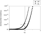
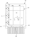
そのうち、周囲光をモニタリングする方法として、公知のUS7218048がある。第1図に示すのは、公知の電子表示装置の構造指示図であり、公知技術では光センサーダイオードを使用し、PIN diodeを光センサー部品とする。この部品は異なる強度の光によって異なる強度の漏電流が発生する。公知技術ではこの特性を利用して周囲の輝度をモニタリングする。しかし、この漏電流の数値は約10乃至8アンペアである。第2図に示すとおり、外部回路はこのように微少の信号を読み取って輝度を修正することができない。そのため、第3図に示すとおり、多数個の光センサーダイオードをひとつに纏め、ひとつに纏めた複数個のトランジスタTSで電流量を蓄積して外部回路がモニタリングする。このため、公知では相当に大きなセンサー面積を必要とし、モニター上の非表示区域を増やすことができないだけではなく、相対してコストが上がる。 Among them, as a method for monitoring ambient light, there is a known US7218048. FIG. 1 shows a structure instruction diagram of a known electronic display device. In the known technique, a photo sensor diode is used, and PIN diode is used as a photo sensor component. In this part, leakage currents with different intensities are generated by different intensities of light. In the known technique, ambient brightness is monitored using this characteristic. However, the value of this leakage current is about 10 to 8 amperes. As shown in FIG. 2, the external circuit cannot read the minute signal in this way and correct the luminance. Therefore, as shown in FIG. 3, a large number of photosensor diodes are combined into one, and the current amount is accumulated by a plurality of transistors TS combined into one, and the external circuit monitors. For this reason, a known sensor area is considerably large, and not only the non-display area on the monitor cannot be increased, but also the cost increases.
公知技術の各問題を改善するため、本発明者は長年の研究開発及び諸々の実務経験を元に、周囲光センサーを備えた液晶ディスプレイ及びその方法を提供して上述の欠点を改善する。 In order to improve the problems of the known art, the present inventor provides a liquid crystal display with an ambient light sensor and a method thereof based on many years of research and development and various practical experiences to improve the above-mentioned drawbacks.
解決しようとする問題点は、相当に大きなセンサー面積を必要とし、モニター上の非表示区域を増やすことができないだけではなく、相対してコストが上がる点である。 The problem to be solved is that it requires a considerably large sensor area and not only can not increase the non-display area on the monitor, but also increases the cost.
本発明は、先ず、一コンデンサーを一薄膜トランジスタの源極に接続する。次に、コンデンサーの電位の電荷が減り、転換するのに要する時間を計算し、その転換時間に基づいて周囲光の強度を計算する。本発明は、別に一種の周囲光センサー回路を提供しており、それは一薄膜トランジスタ、一コンデンサー、及び一読出しスイッチを含む。周囲光が変化した時、薄膜トランジスタの漏電流もそれに従って変化し、コンデンサーの電位転換にかかる転換時間に変化が生じ、読出しスイッチがコンデンサーの電位をデータ読出し線に伝送することによって転換時間から周囲光の強度を算出する。本発明の液晶ディスプレイは複数個のコンデンサー、複数個の読出しスイッチ、及び一処理モジュールを含むことを最も主要な特徴とする。 In the present invention, first, one capacitor is connected to the source electrode of one thin film transistor. Next, the time required for conversion is reduced when the electric potential of the capacitor decreases, and the intensity of ambient light is calculated based on the conversion time. The present invention provides another type of ambient light sensor circuit, which includes one thin film transistor, one capacitor, and one readout switch. When the ambient light changes, the leakage current of the thin film transistor also changes accordingly, causing a change in the conversion time for the capacitor potential change, and the readout switch transmits the capacitor potential to the data readout line, so that the ambient light from the conversion time is changed. The intensity of is calculated. The liquid crystal display according to the present invention is characterized in that it includes a plurality of capacitors, a plurality of readout switches, and a processing module.
本発明の周囲光センサー機能を備えた液晶ディスプレイ及びその方法は、下述の利点がある。
(1) センサー面積を有効に減らす。
(2) 消費電力効率を下げる。
(3) デジタル信号を出力できる。
(4) 生産コストを下げる。
The liquid crystal display having the ambient light sensor function and the method of the present invention have the following advantages.
(1) Effectively reduce the sensor area.
(2) Reduce power consumption efficiency.
(3) A digital signal can be output.
(4) Reduce production costs.
一種の周囲光センサー機能を備えた液晶ディスプレイ及びその方法を提供し、前述の技術に於けるセンサー面積が大きすぎること、コストが高すぎる等の問題を解決することを本発明の目的とする。 It is an object of the present invention to provide a liquid crystal display having a kind of ambient light sensor function and a method therefor, and to solve problems such as the sensor area being too large and the cost being too high in the above-described technology.
本発明の目的に基づき、一種の周囲光センサー方法を提供し、一薄膜トランジスタに適用する。本発明の方法は、先ず、一コンデンサーをこの薄膜トランジスタの源極に接続し、次にそのコンデンサーの電荷を薄膜トランジスタの漏電流に従って減らしていく。そして、そのコンデンサーの電位の電荷が減少して転換するのに要する時間を計算し、最後にその転換時間に基づき周囲光の強度を計算する。 According to the object of the present invention, a kind of ambient light sensor method is provided and applied to one thin film transistor. In the method of the present invention, a capacitor is first connected to the source electrode of the thin film transistor, and then the charge of the capacitor is reduced according to the leakage current of the thin film transistor. Then, the time required for the electric potential of the capacitor to decrease and convert is calculated, and finally the intensity of ambient light is calculated based on the conversion time.
この他、本発明では、一種の周囲光センサー回路を提供し、一ピクセル構造に適用する。それは一薄膜トランジスタ、一コンデンサー、一読出しスイッチを含む。薄膜トランジスタの漏電流の大きさは周囲光の強度と正比例する。コンデンサーの一端は薄膜トランジスタの源極に接続し、別一端はアースとする。一読出しスイッチは薄膜トランジスタの源極と一データ読出し線の間に接続する。そのうち、周囲光が変化した時、薄膜トランジスタの漏電流はそれに従って変化し、またコンデンサーの電位を高電位から低電位へ転換するのに要する転換時間に変化が生じ、読出しスイッチはコンデンサーの電位をデータ読出し線へ伝送し、外部回路はコンデンサーの転換時間に基づき、周囲光の強度を計算する。 In addition, in the present invention, a kind of ambient light sensor circuit is provided and applied to one pixel structure. It includes one thin film transistor, one capacitor, and one readout switch. The magnitude of the leakage current of the thin film transistor is directly proportional to the intensity of ambient light. One end of the capacitor is connected to the source electrode of the thin film transistor, and the other end is grounded. One readout switch is connected between the source electrode of the thin film transistor and one data readout line. Among them, when ambient light changes, the leakage current of the thin film transistor changes accordingly, and the change time required to change the capacitor potential from high potential to low potential changes, and the readout switch changes the capacitor potential to the data Transmitted to the readout line, the external circuit calculates the ambient light intensity based on the capacitor conversion time.
この他、本発明は、更に周囲光に従って一照明モジュールの輝度を調整する一液晶ディスプレイを提供する。それは、複数個のコンデンサー、複数個の読出しスイッチ、及び一処理モジュールを含む。複数個コンデンサーは、液晶ディスプレイの複数個のピクセルに接続する。複数個の読出しスイッチは、これらのコンデンサーと一データ読出し線の間に接続してこれらコンデンサーの電位を読み取る。一処理モジュールは、これらのコンデンサーの電位が高電位から低電位へ転換するのに要する時間に基づいて周囲光の強度を計算し、照明モジュールの輝度を調整する。 In addition, the present invention further provides a liquid crystal display that adjusts the brightness of one illumination module according to ambient light. It includes a plurality of capacitors, a plurality of readout switches, and a processing module. The plurality of capacitors are connected to a plurality of pixels of the liquid crystal display. A plurality of read switches are connected between these capacitors and one data read line to read the potentials of these capacitors. One processing module adjusts the brightness of the lighting module by calculating the intensity of ambient light based on the time required for the potential of these capacitors to change from a high potential to a low potential.
本発明の技術特徴及びその効果を更に理解するため、良好な実施例及び詳細を後述する。 In order to better understand the technical features of the present invention and the effects thereof, preferred embodiments and details are described below.
理解の為に、本発明の実施例の周囲光センサー機能を備えた液晶ディスプレイ及びその方法は図式を参照して説明し、下述の実施例中の同じ部品は、同じ符号で表示して説明をする。 For the sake of understanding, the liquid crystal display having the ambient light sensor function and the method thereof according to the embodiment of the present invention will be described with reference to the drawings, and the same components in the embodiments described below are denoted by the same reference numerals and described. do.
第4図は、本発明の周囲光センサー方法のステップフローチャートである。先ず例としてステップS10に示す本発明の方法は、一コンデンサーを一薄膜トランジスタの源極に接合する。次に、薄膜トランジスタ自身の漏電流は周囲光の強度と正比例するため、ステップS20に示すとおり、このコンデンサーの電荷が上述の薄膜トランジスタの漏電流に従って減る。次にステップS30に示すとおり、コンデンサーの電位の電荷が減少して高電位から低電位へ下がるまでにかかる一転換時間を計算する。最後に、ステップS40に示すとおり、この転換時間の長さによって周囲光の強度を計算する。 FIG. 4 is a step flow chart of the ambient light sensor method of the present invention. First, as an example, in the method of the present invention shown in step S10, one capacitor is joined to the source electrode of one thin film transistor. Next, since the leakage current of the thin film transistor itself is directly proportional to the intensity of ambient light, as shown in step S20, the charge of this capacitor is reduced according to the leakage current of the above-described thin film transistor. Next, as shown in step S30, the conversion time required for the electric charge at the capacitor potential to decrease from the high potential to the low potential is calculated. Finally, as shown in step S40, the intensity of ambient light is calculated based on the length of this conversion time.
言い換えると、本発明の方法は、現行のパネル製造工程によって製造した薄膜トランジスタ部品で、先ず電荷をコンデンサー内に蓄積する。次に薄膜トランジスタが異なる強度の光源照射によって異なる大きさの漏電流特性を有することを利用して、コンデンサー内の電荷流失に必要な時間に差異を発生させる。つまり、周囲光が強い時には、コンデンサーの電位転換に必要な時間が短くなる。パネル上で駆動するスキャン線のクロック信号駆動回路を利用して電位転換信号を読み出し、周囲光の強度をモニタリングする目的を達成する。本発明の方法に使用する部品は現行の製造過程と相互に合致するため、現行のパネル製造過程に於いて、完全に融合し、更には製造過程の変更不要及び低コストの条件により、本発明の目的が達成できる。 In other words, the method of the present invention is a thin film transistor component manufactured by the current panel manufacturing process, and charges are first stored in the capacitor. Next, by utilizing the fact that the thin film transistor has different leakage current characteristics due to irradiation of light sources having different intensities, a difference is generated in the time required for charge flow in the capacitor. That is, when the ambient light is strong, the time required for changing the capacitor potential is shortened. The object of monitoring the intensity of ambient light is achieved by reading out a potential change signal using a clock signal driving circuit of a scan line driven on a panel. Since the parts used in the method of the present invention are mutually compatible with the current manufacturing process, the present invention is completely integrated in the current panel manufacturing process. The purpose of can be achieved.
本発明の方法は、一実施例に於いて、一データ読出し線でコンデンサーの電位を取得する。この他、デジタル化コンデンサーの電位信号のために、本実施例では一ロジックゲートをデータ読出し線に接続する。言い換えると、コンデンサーの電位が一ロジックノットゲートに送られた後、次にデータ読出し線へ出力する。出力信号を明晰にするため、このロジックノットゲートは一反転増幅器によって実現できる。この他、データ読出し線とコンデンサーの間には一読出しスイッチを接続し、液晶パネルに予め設置してあるスキャン線信号を利用して、複数個の読出しスイッチを順に始動し、データ読出し線で複数個のコンデンサーの電位信号を順に取得していく。上述の薄膜トランジスタの漏電流と周囲光が良好な相互関係を備えるため、本実施例の薄膜トランジスタはアモルファスシリコン薄膜トランジスタ、もしくは多結晶薄膜トランジスタを採用する。 The method of the present invention, in one embodiment, acquires the capacitor potential with one data readout line. In addition, one logic gate is connected to the data read line in this embodiment for the potential signal of the digitizing capacitor. In other words, after the potential of the capacitor is sent to one logic knot gate, it is then output to the data read line. In order to clarify the output signal, this logic knot gate can be realized by a inverting amplifier. In addition, one read switch is connected between the data read line and the capacitor, and a plurality of read switches are sequentially started by using a scan line signal previously set on the liquid crystal panel. The potential signal of each capacitor is acquired in order. Since the leakage current and ambient light of the thin film transistor described above have a good correlation, an amorphous silicon thin film transistor or a polycrystalline thin film transistor is employed as the thin film transistor of this embodiment.
第5図に示すのは、本発明の周囲光センサー回路の構造指示図である。本回路は一画素構造に適用し、一入力電圧100、一スキャン線200、一データ読出し線300、感光薄膜トランジスタ400、コンデンサー500、及び読出しスイッチ600を含む。その連接関係は第五図に示すとおりであるため、ここでは詳述しない。そのうち、スキャン線200が感光薄膜トランジスタ400をスタートさせると、入力電圧100がコンデンサー500の電位Vcを高電位まで上げる。スキャン線200が感光薄膜トランジスタ400を停止させると、感光薄膜トランジスタ400は周囲光の照射の下、一漏電流を発生し、且つその漏電流の大きさは、周囲光の強度と正比例するため、その漏電流がコンデンサー500内に保存された電荷を徐々に消耗し、コンデンサー500の電位Vcもまたそれに従い下降する。そして読出しスイッチ600は電位Vcの変化状況をデータ読出し線300へ伝送する。これによって外部回路は電位Vcが高電位から低電位へ転換するための所要時間に基づき、周囲光の強弱を推測する。そのうち、上述の感光薄膜トランジスタ400はアモルファスシリコン薄膜トランジスタ、もしくは多結晶薄膜トランジスタを使用し、良好な周囲光センサー効果を取得する。
FIG. 5 shows a structure instruction diagram of the ambient light sensor circuit of the present invention. This circuit is applied to one pixel structure, and includes one
第6図に示すのは、本発明の周囲光センサー回路の別の構造指示図である。そのうち、本発明は一実施例に於いて、更にコンデンサー500と読出しスイッチ600の間に一反転増幅器700を接続する。コンデンサー500の電位Vcはこの反転増幅器700によって一反転且つ拡大したデジタル信号に転換し、複雑レベルが下がり、正確性が高まる長所を備え、外部回路の周囲光の強度判断が簡単になる。
FIG. 6 shows another structure instruction diagram of the ambient light sensor circuit of the present invention. Among them, in one embodiment of the present invention, an inverting
第7図は、本発明の一実施例の周囲光センサー回路の構造図である。そのうち、読出しスイッチ600は、一薄膜トランジスタスイッチ610に依って実現する。この他、読出しスイッチ600前レベルには一信号拡大トランジスタ620に接続して出力電圧Voutを拡大する。
FIG. 7 is a structural diagram of an ambient light sensor circuit according to an embodiment of the present invention. Among them, the
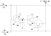
第8図は、本発明の別の一実施例の周囲光センサー回路の構造図である。そのうち、反転増幅器700は、P型薄膜トランジスタ710とN型薄膜トランジスタ720から構成される。その原理は本技術領域内に於いて通常熟知されているものなので詳述しない。読出しスイッチ600は一薄膜トランジスタスイッチ610から構成され、且つ一第二スキャン線220に制御され、これらによって本実施例のすべての部品はすべて現在の製造過程によって実現する。液晶モニターのスキャン信号は第一スキャン線210と第二スキャン線220に順に送られるため、光薄膜トランジスタ400と薄膜トランジスタスイッチ610が順に始動する。そのため、データ読出し線300は出力電圧Voutの波形を順に取得する。第9図に示すとおり、データ読出し線300はスキャン信号をベースバンドとして、出力電圧信号の電位転換時間の長さを計算する。例として、強光照射では出力電圧Voutが一個のベースバンド内で高電位から低電位へ転換する。また周囲光が弱い時には、出力電圧Voutが2〜3個のベースバンドを経て初めて転換する。
FIG. 8 is a structural diagram of an ambient light sensor circuit according to another embodiment of the present invention. Among them, the inverting
第10図は、本発明の液晶ディスプレイの構造指示図であり、一処理モジュール810、一照明モジュール820、一パネル900、一データ読出し線300、複数の読出しスイッチ600、複数のコンデンサー500と複数のピクセル830を含む。周知のとおり、パネル900自身は相当数のピクセル構造を備え、ユーザーは製造過程の必要、もしくはコスト面によって一部もしくはすべてのピクセル830をコンデンサー500と読出しスイッチ600に接続することを考慮することができる。ピクセル830内の薄膜トランジスタは、周囲光が照射されることにより、漏電流が発生した時、コンデンサー500の電位は漏電流が途切れることなくコンデンサー500の電荷へ移動するのに従い下降する。処理モジュール810が読出しスイッチ600を順に始動し、コンデンサー500の電位信号がデータ読出し線300に伝送され、処理モジュール810がデータ読出し線300の取得を通して周囲光強弱を代表するコンデンサー電位転換時間を取得すると、照明モジュール820の強度、例としてバックライトモジュールを調整することができ、消費電力節約の目的を達成することができる。この他、コンデンサー500の電位信号を拡大するために鑑別度及びデジタル化した上述の電位転換時間を増やすことによってコンデンサー500は一ロジックノットゲート、例として一反転増幅器700を接続することができる。
FIG. 10 is a diagram showing the structure of the liquid crystal display according to the present invention. One
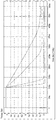
次に第11図に示すのは、本発明のバーチャル波形図である。このバーチャル波形は、異なる強度の周囲光照射によってTFTトランジスタ漏電流の大きさをバーチャルする。第12図に示すのは本発明の一実施例の実測波形図で、第一スキャン線信号と入力電圧信号作動を実測した後、異なる強度の周囲光照射の下でTFTトランジスタ漏電流の大きさ状態である。 Next, FIG. 11 shows a virtual waveform diagram of the present invention. This virtual waveform virtualizes the magnitude of the TFT transistor leakage current by irradiation with ambient light of different intensity. FIG. 12 is an actually measured waveform diagram of one embodiment of the present invention. After actually measuring the first scan line signal and input voltage signal operation, the magnitude of the TFT transistor leakage current under ambient light irradiation of different intensity. State.
本発明は、薄膜トランジスタの漏電流の大きさと周囲光の強度が正比例することを利用して周囲光の変化をモニタリングするものであるが、これを制限するものではない。仮に薄膜トランジスタの漏電流の大きさと周囲光の強度が反比例しても本発明の周囲光モニタリングの目的は遂行され、本発明が薄膜トランジスタの漏電流を利用して周囲光をモニタリングする精神から乖離しない。このため、上述の薄膜トランジスタはアモルファスシリコン薄膜トランジスタ、もしくは多結晶薄膜トランジスタがよいが、これを制限するものではない。 The present invention monitors the change in ambient light by utilizing the fact that the magnitude of the leakage current of the thin film transistor and the intensity of ambient light are directly proportional, but this is not a limitation. Even if the magnitude of the leakage current of the thin film transistor and the intensity of the ambient light are inversely proportional, the purpose of the ambient light monitoring of the present invention is achieved, and the present invention does not depart from the spirit of monitoring the ambient light using the leakage current of the thin film transistor. For this reason, the above-mentioned thin film transistor is preferably an amorphous silicon thin film transistor or a polycrystalline thin film transistor, but is not limited thereto.
上述の通り、本発明の周囲光センサー機能を備えた液晶ディスプレイ及びその方法は下述の特色を備える。
1.現行の製造過程に依る薄膜トランジスタを周囲光センサー器とすることができる。
2.センサー面積を減らすことができる。
3.消耗率を下げることができる。
4.生産コストを下げることができる。
5.デジタル信号出力できる。
As described above, the liquid crystal display having the ambient light sensor function and the method of the present invention have the following features.
1. A thin film transistor according to the current manufacturing process can be used as an ambient light sensor device.
2. The sensor area can be reduced.
3. The consumption rate can be lowered.
4). Production costs can be reduced.
5). Digital signal output is possible.
S10〜S40 ステップ
100 入力電圧
200 スキャン線
210 第一スキャン線
220 第二スキャン線
300 データ読出し線
400 感光薄膜トランジスタ
500 コンデンサー
600 読出しスイッチ
610 薄膜トランジスタスイッチ
620 信号拡大トランジスタ
700 反転増幅器
710 P型薄膜トランジスタ
720 N型薄膜トランジスタ
810 処理モジュール
820 照明モジュール
830 ピクセル
900 パネル
Steps S10 to
720 N-type
Claims (14)
一コンデンサーを前記薄膜トランジスタの源極に接続し、
前記コンデンサーの電荷を前記薄膜トランジスタの漏電流に従って減らし、
前記コンデンサーの電位の電荷が減少することによって発生する転換に要する一転換時間を計算し、かつ
前記転換時間に基づき前記周囲光の強度を計算することを含むことを特徴とする周囲光センサーの方法。 In an ambient light sensor method applied to a thin film transistor, the method includes connecting a capacitor to a source electrode of the thin film transistor;
Reducing the charge of the capacitor according to the leakage current of the thin film transistor;
A method of ambient light sensor comprising: calculating a conversion time required for conversion generated by a decrease in electric charge of the capacitor potential; and calculating the intensity of the ambient light based on the conversion time .
漏電流と前記周囲光が正比例する一薄膜トランジスタと、
一端を前記薄膜トランジスタの源極に接続し、別一端はアースとする一コンデンサーと、
前記薄膜トランジスタの源極と一データ読出し線の間に接続する一読出しスイッチを含み、そのうち、
周囲光が変化した時、前記薄膜トランジスタの漏電流もまたその変化に従い、前記コンデンサーの電位転換に要する一転換時間に変化を発生させ、前記読出しスイッチは前記コンデンサーの電位を前記データ読出し線へ伝送することを特徴とする周囲光センサー回路。 In a kind of ambient light sensor circuit applied to one pixel structure,
A thin film transistor in which the leakage current and the ambient light are directly proportional;
One capacitor is connected to the source electrode of the thin film transistor and the other end is grounded.
Including one readout switch connected between the source electrode of the thin film transistor and one data readout line,
When ambient light changes, the leakage current of the thin film transistor also changes according to the change, causing a change in the conversion time required for changing the potential of the capacitor, and the readout switch transmits the potential of the capacitor to the data readout line. Ambient light sensor circuit characterized by that.
前記液晶ディスプレイの複数個のピクセルに接続する複数のコンデンサーと、
前記複数のコンデンサーと一データ読出し線の間に接続してこれらコンデンサーの電位を読み取る複数個読出しスイッチと、
前記複数のコンデンサーの電位転換に要する時間に基づき、前記周囲光の強度を計算し、前記照明モジュールの輝度を調整する一処理モジュールを含むことを特徴とする液晶ディスプレイ。 In a kind of liquid crystal display that adjusts the brightness of one illumination module according to one ambient light,
A plurality of capacitors connected to a plurality of pixels of the liquid crystal display;
A plurality of readout switches connected between the plurality of capacitors and one data readout line to read the potentials of these capacitors;
A liquid crystal display comprising: a processing module that calculates the intensity of the ambient light and adjusts the luminance of the illumination module based on the time required for changing the potential of the plurality of capacitors.
Applications Claiming Priority (1)
| Application Number | Priority Date | Filing Date | Title |
|---|---|---|---|
| TW096145046A TWI358570B (en) | 2007-11-27 | 2007-11-27 | Lcd with ambient light sense function and method t |
Publications (1)
| Publication Number | Publication Date |
|---|---|
| JP2009128902A true JP2009128902A (en) | 2009-06-11 |
Family
ID=40669397
Family Applications (1)
| Application Number | Title | Priority Date | Filing Date |
|---|---|---|---|
| JP2008127593A Pending JP2009128902A (en) | 2007-11-27 | 2008-05-14 | Liquid crystal display with ambient light sensor function and method thereof |
Country Status (4)
| Country | Link |
|---|---|
| US (1) | US20090135333A1 (en) |
| JP (1) | JP2009128902A (en) |
| KR (1) | KR20090054879A (en) |
| TW (1) | TWI358570B (en) |
Cited By (1)
| Publication number | Priority date | Publication date | Assignee | Title |
|---|---|---|---|---|
| CN111179870A (en) * | 2020-01-31 | 2020-05-19 | 北京京东方显示技术有限公司 | A power supply driving circuit, its driving method and display device |
Families Citing this family (7)
| Publication number | Priority date | Publication date | Assignee | Title |
|---|---|---|---|---|
| CN101609855B (en) * | 2008-06-20 | 2013-09-18 | 群康科技(深圳)有限公司 | Photosensitive capacitor, photosensitive circuit, substrate, manufacturing process thereof and display device |
| TWI428906B (en) | 2009-09-30 | 2014-03-01 | Toshiba Global Commerce Solutions Holdings Corp | Method of automatically adjusting a brightness of an optical touch panel and apparatus thereof |
| US8626236B2 (en) | 2010-10-08 | 2014-01-07 | Blackberry Limited | System and method for displaying text in augmented reality |
| KR101874034B1 (en) | 2012-02-10 | 2018-07-06 | 삼성디스플레이 주식회사 | Optical sensor, display device including the same and driving method thereof |
| TWI460841B (en) * | 2012-07-13 | 2014-11-11 | Au Optronics Corp | Photo sensor type touch display panel |
| CN108320719B (en) * | 2018-02-28 | 2021-01-15 | 京东方科技集团股份有限公司 | Pixel charging method, display panel and display device |
| CN112530352B (en) * | 2020-12-24 | 2023-07-25 | 武汉天马微电子有限公司 | Driving method and driving device of a display device |
Citations (6)
| Publication number | Priority date | Publication date | Assignee | Title |
|---|---|---|---|---|
| JP2002077521A (en) * | 2000-08-28 | 2002-03-15 | Casio Comput Co Ltd | Two-dimensional image reading apparatus and sensitivity correction method thereof |
| JP2006163401A (en) * | 2004-12-03 | 2006-06-22 | Samsung Electronics Co Ltd | Display device with built-in light sensor |
| JP2007011152A (en) * | 2005-07-01 | 2007-01-18 | Toshiba Matsushita Display Technology Co Ltd | Flat display device |
| JP2007065243A (en) * | 2005-08-31 | 2007-03-15 | Sanyo Epson Imaging Devices Corp | Display device |
| JP2007114315A (en) * | 2005-10-18 | 2007-05-10 | Toshiba Matsushita Display Technology Co Ltd | Display device |
| JP2008070616A (en) * | 2006-09-14 | 2008-03-27 | Epson Imaging Devices Corp | Electro-optical device and method of determining its optical sensor failure |
Family Cites Families (10)
| Publication number | Priority date | Publication date | Assignee | Title |
|---|---|---|---|---|
| SG111910A1 (en) * | 2000-09-07 | 2005-06-29 | Agilent Technologies Inc | Transceiver module |
| US7061480B2 (en) * | 2002-04-30 | 2006-06-13 | Hewlett-Packard Development Company, L.P. | Image display |
| KR100957585B1 (en) * | 2003-10-15 | 2010-05-13 | 삼성전자주식회사 | Electronic display device having a light sensing unit |
| US6975008B2 (en) * | 2003-10-27 | 2005-12-13 | Eastman Kodak Company | Circuit for detecting ambient light on a display |
| KR100997977B1 (en) * | 2004-01-12 | 2010-12-02 | 삼성전자주식회사 | Optical sensor and display device using same |
| TWI261140B (en) * | 2005-05-31 | 2006-09-01 | Au Optronics Corp | Display panels |
| US20070109239A1 (en) * | 2005-11-14 | 2007-05-17 | Den Boer Willem | Integrated light sensitive liquid crystal display |
| US7655889B2 (en) * | 2006-05-24 | 2010-02-02 | Toshiba Matsushita Display Technology Co., Ltd. | Display device and control method therefor |
| US7623112B2 (en) * | 2006-06-14 | 2009-11-24 | Hannstar Display Corp. | Image sensor array and liquid crystal display with sensor elements |
| KR100878379B1 (en) * | 2006-07-12 | 2009-01-13 | 엡슨 이미징 디바이스 가부시키가이샤 | Liquid crystal display |
-
2007
- 2007-11-27 TW TW096145046A patent/TWI358570B/en active
-
2008
- 2008-03-03 KR KR1020080019800A patent/KR20090054879A/en not_active Ceased
- 2008-03-06 US US12/073,485 patent/US20090135333A1/en not_active Abandoned
- 2008-05-14 JP JP2008127593A patent/JP2009128902A/en active Pending
Patent Citations (6)
| Publication number | Priority date | Publication date | Assignee | Title |
|---|---|---|---|---|
| JP2002077521A (en) * | 2000-08-28 | 2002-03-15 | Casio Comput Co Ltd | Two-dimensional image reading apparatus and sensitivity correction method thereof |
| JP2006163401A (en) * | 2004-12-03 | 2006-06-22 | Samsung Electronics Co Ltd | Display device with built-in light sensor |
| JP2007011152A (en) * | 2005-07-01 | 2007-01-18 | Toshiba Matsushita Display Technology Co Ltd | Flat display device |
| JP2007065243A (en) * | 2005-08-31 | 2007-03-15 | Sanyo Epson Imaging Devices Corp | Display device |
| JP2007114315A (en) * | 2005-10-18 | 2007-05-10 | Toshiba Matsushita Display Technology Co Ltd | Display device |
| JP2008070616A (en) * | 2006-09-14 | 2008-03-27 | Epson Imaging Devices Corp | Electro-optical device and method of determining its optical sensor failure |
Cited By (1)
| Publication number | Priority date | Publication date | Assignee | Title |
|---|---|---|---|---|
| CN111179870A (en) * | 2020-01-31 | 2020-05-19 | 北京京东方显示技术有限公司 | A power supply driving circuit, its driving method and display device |
Also Published As
| Publication number | Publication date |
|---|---|
| TWI358570B (en) | 2012-02-21 |
| TW200923476A (en) | 2009-06-01 |
| US20090135333A1 (en) | 2009-05-28 |
| KR20090054879A (en) | 2009-06-01 |
Similar Documents
| Publication | Publication Date | Title |
|---|---|---|
| KR101721854B1 (en) | Display device and electronic device | |
| JP4488011B2 (en) | Electro-optical device, semiconductor device, display device, and electronic apparatus including the same | |
| TWI779845B (en) | Pixel circuit and driving method, display panel, and display device | |
| US10719169B2 (en) | Touch readout circuit, touch display panel and display device | |
| CN102314840B (en) | Image sensor, electronic device and backlight adjusting method thereof | |
| TWI358570B (en) | Lcd with ambient light sense function and method t | |
| CN201122422Y (en) | LCD device | |
| CN108346400B (en) | Pixel circuit, driving method and display panel | |
| JP4814028B2 (en) | Liquid crystal display | |
| CN107680522A (en) | A kind of display panel testing method and its device | |
| CN115917637B (en) | Brightness control device, method and display device | |
| CN203870951U (en) | Pixel circuit, organic light-emitting display panel, and display device | |
| CN116524864B (en) | A pixel circuit, its driving method, and a display device | |
| CN217113806U (en) | Display screen with embedded temperature sensing function | |
| US20080284757A1 (en) | Light pointing device employed in input apparatus, driving method and input apparatus using the same | |
| JP2007205902A (en) | Light detecting circuit, electro-optical device, and electronic equipment | |
| CN100580754C (en) | Optical detection device, liquid crystal display using same and driving method thereof | |
| TW202303561A (en) | Pixel circuit and driving method therefor, display substrate, and display apparatus | |
| CN107507589A (en) | A kind of charge/discharge control circuit and method, the display device of control sub-pix electric discharge | |
| CN201742481U (en) | Image sensor and electronic equipment | |
| CN103091886A (en) | Liquid crystal display device and liquid crystal panel thereof | |
| US8269753B2 (en) | Display device and electronic machine having the same | |
| CN115410542A (en) | Display panel and display device | |
| JP2009212964A (en) | Photo-sensor incorporated mobile terminal and photometric control method of the photo-sensor incorporated mobile terminal | |
| KR20080083932A (en) | Sensor circuit and driving method of the sensor circuit |
Legal Events
| Date | Code | Title | Description |
|---|---|---|---|
| A131 | Notification of reasons for refusal |
Free format text: JAPANESE INTERMEDIATE CODE: A131 Effective date: 20110329 |
|
| A521 | Request for written amendment filed |
Free format text: JAPANESE INTERMEDIATE CODE: A523 Effective date: 20110629 |
|
| A131 | Notification of reasons for refusal |
Free format text: JAPANESE INTERMEDIATE CODE: A131 Effective date: 20111018 |
|
| A521 | Request for written amendment filed |
Free format text: JAPANESE INTERMEDIATE CODE: A523 Effective date: 20120106 |
|
| A131 | Notification of reasons for refusal |
Free format text: JAPANESE INTERMEDIATE CODE: A131 Effective date: 20120410 |
|
| A02 | Decision of refusal |
Free format text: JAPANESE INTERMEDIATE CODE: A02 Effective date: 20121113 |