JP2009129973A - 窒化物半導体発光素子の製造方法 - Google Patents
窒化物半導体発光素子の製造方法 Download PDFInfo
- Publication number
- JP2009129973A JP2009129973A JP2007300602A JP2007300602A JP2009129973A JP 2009129973 A JP2009129973 A JP 2009129973A JP 2007300602 A JP2007300602 A JP 2007300602A JP 2007300602 A JP2007300602 A JP 2007300602A JP 2009129973 A JP2009129973 A JP 2009129973A
- Authority
- JP
- Japan
- Prior art keywords
- nitride semiconductor
- layer
- type
- electrode
- manufacturing
- Prior art date
- Legal status (The legal status is an assumption and is not a legal conclusion. Google has not performed a legal analysis and makes no representation as to the accuracy of the status listed.)
- Granted
Links
Images




Classifications
-
- H—ELECTRICITY
- H01—ELECTRIC ELEMENTS
- H01S—DEVICES USING THE PROCESS OF LIGHT AMPLIFICATION BY STIMULATED EMISSION OF RADIATION [LASER] TO AMPLIFY OR GENERATE LIGHT; DEVICES USING STIMULATED EMISSION OF ELECTROMAGNETIC RADIATION IN WAVE RANGES OTHER THAN OPTICAL
- H01S5/00—Semiconductor lasers
- H01S5/20—Structure or shape of the semiconductor body to guide the optical wave ; Confining structures perpendicular to the optical axis, e.g. index or gain guiding, stripe geometry, broad area lasers, gain tailoring, transverse or lateral reflectors, special cladding structures, MQW barrier reflection layers
- H01S5/22—Structure or shape of the semiconductor body to guide the optical wave ; Confining structures perpendicular to the optical axis, e.g. index or gain guiding, stripe geometry, broad area lasers, gain tailoring, transverse or lateral reflectors, special cladding structures, MQW barrier reflection layers having a ridge or stripe structure
-
- B—PERFORMING OPERATIONS; TRANSPORTING
- B82—NANOTECHNOLOGY
- B82Y—SPECIFIC USES OR APPLICATIONS OF NANOSTRUCTURES; MEASUREMENT OR ANALYSIS OF NANOSTRUCTURES; MANUFACTURE OR TREATMENT OF NANOSTRUCTURES
- B82Y20/00—Nanooptics, e.g. quantum optics or photonic crystals
-
- H—ELECTRICITY
- H01—ELECTRIC ELEMENTS
- H01S—DEVICES USING THE PROCESS OF LIGHT AMPLIFICATION BY STIMULATED EMISSION OF RADIATION [LASER] TO AMPLIFY OR GENERATE LIGHT; DEVICES USING STIMULATED EMISSION OF ELECTROMAGNETIC RADIATION IN WAVE RANGES OTHER THAN OPTICAL
- H01S2301/00—Functional characteristics
- H01S2301/17—Semiconductor lasers comprising special layers
- H01S2301/173—The laser chip comprising special buffer layers, e.g. dislocation prevention or reduction
-
- H—ELECTRICITY
- H01—ELECTRIC ELEMENTS
- H01S—DEVICES USING THE PROCESS OF LIGHT AMPLIFICATION BY STIMULATED EMISSION OF RADIATION [LASER] TO AMPLIFY OR GENERATE LIGHT; DEVICES USING STIMULATED EMISSION OF ELECTROMAGNETIC RADIATION IN WAVE RANGES OTHER THAN OPTICAL
- H01S2304/00—Special growth methods for semiconductor lasers
- H01S2304/04—MOCVD or MOVPE
-
- H—ELECTRICITY
- H01—ELECTRIC ELEMENTS
- H01S—DEVICES USING THE PROCESS OF LIGHT AMPLIFICATION BY STIMULATED EMISSION OF RADIATION [LASER] TO AMPLIFY OR GENERATE LIGHT; DEVICES USING STIMULATED EMISSION OF ELECTROMAGNETIC RADIATION IN WAVE RANGES OTHER THAN OPTICAL
- H01S5/00—Semiconductor lasers
- H01S5/0014—Measuring characteristics or properties thereof
- H01S5/0021—Degradation or life time measurements
-
- H—ELECTRICITY
- H01—ELECTRIC ELEMENTS
- H01S—DEVICES USING THE PROCESS OF LIGHT AMPLIFICATION BY STIMULATED EMISSION OF RADIATION [LASER] TO AMPLIFY OR GENERATE LIGHT; DEVICES USING STIMULATED EMISSION OF ELECTROMAGNETIC RADIATION IN WAVE RANGES OTHER THAN OPTICAL
- H01S5/00—Semiconductor lasers
- H01S5/04—Processes or apparatus for excitation, e.g. pumping, e.g. by electron beams
- H01S5/042—Electrical excitation ; Circuits therefor
- H01S5/0425—Electrodes, e.g. characterised by the structure
- H01S5/04252—Electrodes, e.g. characterised by the structure characterised by the material
-
- H—ELECTRICITY
- H01—ELECTRIC ELEMENTS
- H01S—DEVICES USING THE PROCESS OF LIGHT AMPLIFICATION BY STIMULATED EMISSION OF RADIATION [LASER] TO AMPLIFY OR GENERATE LIGHT; DEVICES USING STIMULATED EMISSION OF ELECTROMAGNETIC RADIATION IN WAVE RANGES OTHER THAN OPTICAL
- H01S5/00—Semiconductor lasers
- H01S5/20—Structure or shape of the semiconductor body to guide the optical wave ; Confining structures perpendicular to the optical axis, e.g. index or gain guiding, stripe geometry, broad area lasers, gain tailoring, transverse or lateral reflectors, special cladding structures, MQW barrier reflection layers
- H01S5/2004—Confining in the direction perpendicular to the layer structure
- H01S5/2009—Confining in the direction perpendicular to the layer structure by using electron barrier layers
-
- H—ELECTRICITY
- H01—ELECTRIC ELEMENTS
- H01S—DEVICES USING THE PROCESS OF LIGHT AMPLIFICATION BY STIMULATED EMISSION OF RADIATION [LASER] TO AMPLIFY OR GENERATE LIGHT; DEVICES USING STIMULATED EMISSION OF ELECTROMAGNETIC RADIATION IN WAVE RANGES OTHER THAN OPTICAL
- H01S5/00—Semiconductor lasers
- H01S5/30—Structure or shape of the active region; Materials used for the active region
- H01S5/32—Structure or shape of the active region; Materials used for the active region comprising PN junctions, e.g. hetero- or double- heterostructures
- H01S5/3211—Structure or shape of the active region; Materials used for the active region comprising PN junctions, e.g. hetero- or double- heterostructures characterised by special cladding layers, e.g. details on band-discontinuities
- H01S5/3213—Structure or shape of the active region; Materials used for the active region comprising PN junctions, e.g. hetero- or double- heterostructures characterised by special cladding layers, e.g. details on band-discontinuities asymmetric clading layers
-
- H—ELECTRICITY
- H01—ELECTRIC ELEMENTS
- H01S—DEVICES USING THE PROCESS OF LIGHT AMPLIFICATION BY STIMULATED EMISSION OF RADIATION [LASER] TO AMPLIFY OR GENERATE LIGHT; DEVICES USING STIMULATED EMISSION OF ELECTROMAGNETIC RADIATION IN WAVE RANGES OTHER THAN OPTICAL
- H01S5/00—Semiconductor lasers
- H01S5/30—Structure or shape of the active region; Materials used for the active region
- H01S5/34—Structure or shape of the active region; Materials used for the active region comprising quantum well or superlattice structures, e.g. single quantum well [SQW] lasers, multiple quantum well [MQW] lasers or graded index separate confinement heterostructure [GRINSCH] lasers
- H01S5/343—Structure or shape of the active region; Materials used for the active region comprising quantum well or superlattice structures, e.g. single quantum well [SQW] lasers, multiple quantum well [MQW] lasers or graded index separate confinement heterostructure [GRINSCH] lasers in AIIIBV compounds, e.g. AlGaAs-laser, InP-based laser
- H01S5/34333—Structure or shape of the active region; Materials used for the active region comprising quantum well or superlattice structures, e.g. single quantum well [SQW] lasers, multiple quantum well [MQW] lasers or graded index separate confinement heterostructure [GRINSCH] lasers in AIIIBV compounds, e.g. AlGaAs-laser, InP-based laser with a well layer based on Ga(In)N or Ga(In)P, e.g. blue laser
-
- H—ELECTRICITY
- H10—SEMICONDUCTOR DEVICES; ELECTRIC SOLID-STATE DEVICES NOT OTHERWISE PROVIDED FOR
- H10H—INORGANIC LIGHT-EMITTING SEMICONDUCTOR DEVICES HAVING POTENTIAL BARRIERS
- H10H20/00—Individual inorganic light-emitting semiconductor devices having potential barriers, e.g. light-emitting diodes [LED]
- H10H20/80—Constructional details
- H10H20/81—Bodies
- H10H20/822—Materials of the light-emitting regions
- H10H20/824—Materials of the light-emitting regions comprising only Group III-V materials, e.g. GaP
- H10H20/825—Materials of the light-emitting regions comprising only Group III-V materials, e.g. GaP containing nitrogen, e.g. GaN
-
- H—ELECTRICITY
- H10—SEMICONDUCTOR DEVICES; ELECTRIC SOLID-STATE DEVICES NOT OTHERWISE PROVIDED FOR
- H10H—INORGANIC LIGHT-EMITTING SEMICONDUCTOR DEVICES HAVING POTENTIAL BARRIERS
- H10H20/00—Individual inorganic light-emitting semiconductor devices having potential barriers, e.g. light-emitting diodes [LED]
- H10H20/80—Constructional details
- H10H20/83—Electrodes
- H10H20/832—Electrodes characterised by their material
Landscapes
- Physics & Mathematics (AREA)
- Engineering & Computer Science (AREA)
- Nanotechnology (AREA)
- Optics & Photonics (AREA)
- Chemical & Material Sciences (AREA)
- Crystallography & Structural Chemistry (AREA)
- Biophysics (AREA)
- Life Sciences & Earth Sciences (AREA)
- Geometry (AREA)
- Condensed Matter Physics & Semiconductors (AREA)
- General Physics & Mathematics (AREA)
- Electromagnetism (AREA)
- Semiconductor Lasers (AREA)
- Led Devices (AREA)
Abstract
【解決手段】GaN単結晶基板1上にp型GaNコンタクト層11等が積層された半導体積層構造を形成する。p型GaNコンタクト層11上に、Pd層16とTa層17とを有するp型電極15を形成する。p型電極15を形成した後に、酸素を含む雰囲気中において温度400℃〜600℃で熱処理を行う。熱処理を行った後に、p型電極15上に、Auを含むパッド電極18を形成する。
【選択図】図1
Description
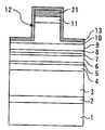
図1は、実施の形態1に係る窒化物半導体レーザダイオードを示す断面図である。GaN基板1(基板)の一主面であるGa面上に、n型GaNバッファ層2が形成されている。このn型GaNバッファ層2は、GaN基板1表面の凹凸を低減し、その上層をできるだけ平坦に積層するために形成されている。そして、このn型GaNバッファ層2上に、n型AlGaNクラッド層3が形成されている。
まず、図2に示すように、予めサーマルクリーニングなどにより表面を清浄化したGaN基板1のGa面上に、有機金属化学気相成長(MOCVD)法により、例えば成長温度1000℃でn型GaNバッファ層2を成長させる。次に、MOCVD法により、n型AlGaNクラッド層3、n型GaN光ガイド層4及びアンドープInGaN光ガイド層5、アンドープのInxGa1−xN/InyGa1−yN多重量子井戸活性層6、アンドープInGaN光導波層7、p型AlGaN電子障壁層8、p型GaN光ガイド層9、p型AlGaNクラッド層10、及びp型GaNコンタクト層11を順次積層する。ここで、例えば、n型AlGaNクラッド層3及びn型GaN光ガイド層4の成長温度を1000℃、アンドープInGaN光導波層7からアンドープInGaN光導波層7の成長温度を740℃、p型AlGaN電子障壁層8からp型GaNコンタクト層11の成長温度を1000℃とする。
実施の形態2に係る窒化物半導体発光素子の製造方法について説明する。
まず、実施の形態1と同様に、図2に示すようにGaN基板1上に窒化物半導体エピ層を形成する。
次に、図15に示すように、上記の結晶成長を行ったウェハ全面にレジストを塗布し、リソグラフィー法(写真製版技術)により所定形状のレジストパターン21を形成する。
次に、全面にレジスト(不図示)を形成する。そして、図18に示すように、エッチバックによりリッジ12の上面においてSiO2膜13を除去して開口14を形成する。その後、実施の形態1と同様に熱処理を行う。
上記実施の形態では、窒化物半導体レーザダイオードを例にして説明したが、本発明はこれに限定されるものではなく、発光ダイオード(LED)等のレーザダイオード以外の窒化物半導体発光素子にも適応することができる。
11 p型GaNコンタクト層(p型窒化物半導体エピ層)
12 リッジ
13 SiO2膜(絶縁膜)
14 開口
15 p型電極
16 Pd層(第1電極層)
17 Ta層(第2電極層)
18 パッド電極
19 n型電極
Claims (11)
- 基板上に、n型窒化物半導体エピ層、活性層、p型窒化物半導体エピ層が積層された半導体積層構造を形成する工程と、
前記p型窒化物半導体エピ層上に、Pdを含む第1電極層とTaを含む第2電極層とを有するp型電極を形成する工程と、
前記p型電極を形成した後に、酸素を含む雰囲気中において400℃〜600℃で熱処理を行う工程と、
前記熱処理を行った後に、前記p型電極上に、Auを含むパッド電極を形成する工程とを備えることを特徴とする窒化物半導体発光素子の製造方法。 - 前記熱処理を450〜550℃で行うことを特徴とする請求項1に記載の窒化物半導体発光素子の製造方法。
- 前記基板としてGaN単結晶基板を用い、
前記半導体積層構造を前記GaN単結晶基板のGa面上に形成することを特徴とする請求項1又は2に記載の窒化物半導体発光素子の製造方法。 - 前記第1電極層の厚みを前記第2電極層の厚みの少なくとも2倍以上とすることを特徴とする請求項1〜3の何れか1項に記載の窒化物半導体発光素子の製造方法。
- 前記第1電極層の厚みを30nm以上とすることを特徴とする請求項4に記載の窒化物半導体発光素子の製造方法。
- 前記第1電極層としてPdTa合金を用いることを特徴とする請求項1〜5の何れか1項に記載の窒化物半導体発光素子の製造方法。
- 前記熱処理において、温度上昇速度を10℃/sec以上とすることを特徴とする請求項1〜6の何れか1項に記載の窒化物半導体発光素子の製造方法。
- 前記雰囲気として、酸素又は酸素を構成元素として含むガスと不活性ガスとの混合ガスであって、酸素含有量が5%以上50%未満であるガスを用いることを特徴とする請求項1〜7の何れか1項に記載の窒化物半導体発光素子の製造方法。
- 前記p型窒化物半導体エピ層が、キャリア濃度が2E17cm−3以上のコンタクト層を含み、
前記コンタクト層上に前記第1電極層を形成することを特徴とする請求項1〜8の何れか1項に記載の窒化物半導体発光素子の製造方法。 - 前記基板の裏面にプラズマ処理を行った後にn型電極を形成し、400℃以下で熱処理を行う工程を更に有することを特徴とする請求項1〜9の何れか1項に記載の窒化物半導体発光素子の製造方法。
- 前記p型電極を形成する工程の後、前記p型電極と前記p型窒化物半導体エピ層を異方性エッチングしてリッジを形成する工程と、
前記リッジを覆うように絶縁膜を形成する工程とを更に備えることを特徴とすることを特徴とする請求項1〜10の何れか1項に記載の窒化物半導体発光素子の製造方法。
Priority Applications (4)
| Application Number | Priority Date | Filing Date | Title |
|---|---|---|---|
| JP2007300602A JP4952534B2 (ja) | 2007-11-20 | 2007-11-20 | 窒化物半導体発光素子の製造方法 |
| TW097138536A TWI397196B (zh) | 2007-11-20 | 2008-10-07 | 氮化物半導體發光元件之製造方法 |
| US12/264,976 US7964424B2 (en) | 2007-11-20 | 2008-11-05 | Method for manufacturing nitride semiconductor light-emitting element |
| CN2008101768041A CN101442094B (zh) | 2007-11-20 | 2008-11-19 | 氮化物半导体发光元件的制造方法 |
Applications Claiming Priority (1)
| Application Number | Priority Date | Filing Date | Title |
|---|---|---|---|
| JP2007300602A JP4952534B2 (ja) | 2007-11-20 | 2007-11-20 | 窒化物半導体発光素子の製造方法 |
Publications (2)
| Publication Number | Publication Date |
|---|---|
| JP2009129973A true JP2009129973A (ja) | 2009-06-11 |
| JP4952534B2 JP4952534B2 (ja) | 2012-06-13 |
Family
ID=40642394
Family Applications (1)
| Application Number | Title | Priority Date | Filing Date |
|---|---|---|---|
| JP2007300602A Expired - Fee Related JP4952534B2 (ja) | 2007-11-20 | 2007-11-20 | 窒化物半導体発光素子の製造方法 |
Country Status (4)
| Country | Link |
|---|---|
| US (1) | US7964424B2 (ja) |
| JP (1) | JP4952534B2 (ja) |
| CN (1) | CN101442094B (ja) |
| TW (1) | TWI397196B (ja) |
Cited By (3)
| Publication number | Priority date | Publication date | Assignee | Title |
|---|---|---|---|---|
| WO2010147181A1 (ja) * | 2009-06-19 | 2010-12-23 | 住友電気工業株式会社 | Iii族窒化物半導体レーザダイオード |
| JP2012069777A (ja) * | 2010-09-24 | 2012-04-05 | Sumitomo Electric Ind Ltd | 半導体発光素子の製造方法 |
| CN110165025A (zh) * | 2019-03-29 | 2019-08-23 | 华灿光电(苏州)有限公司 | 发光二极管芯片、发光二极管及其制作方法 |
Families Citing this family (7)
| Publication number | Priority date | Publication date | Assignee | Title |
|---|---|---|---|---|
| JP5258275B2 (ja) * | 2007-12-07 | 2013-08-07 | 三菱電機株式会社 | 窒化物半導体装置およびその製造方法 |
| WO2011052437A1 (en) | 2009-10-30 | 2011-05-05 | Semiconductor Energy Laboratory Co., Ltd. | Non-linear element, display device including non-linear element, and electronic device including display device |
| JP2011165869A (ja) * | 2010-02-09 | 2011-08-25 | Mitsubishi Electric Corp | 半導体発光素子及びその製造方法 |
| US20150037917A1 (en) * | 2012-04-24 | 2015-02-05 | Panasonic Corporation | Method for manufacturing light-emitting element |
| JP6152848B2 (ja) * | 2012-07-06 | 2017-06-28 | パナソニックIpマネジメント株式会社 | 半導体発光素子 |
| CN104600165B (zh) * | 2015-02-06 | 2018-03-23 | 安徽三安光电有限公司 | 一种氮化物发光二极体结构 |
| CN113488531A (zh) * | 2021-07-14 | 2021-10-08 | 南方科技大学 | P型氮化镓基器件、其欧姆接触系统、及其电极制备方法 |
Citations (8)
| Publication number | Priority date | Publication date | Assignee | Title |
|---|---|---|---|---|
| JPH10308534A (ja) * | 1997-05-08 | 1998-11-17 | Showa Denko Kk | 発光半導体素子用透光性電極およびその作製方法 |
| JP2002246689A (ja) * | 2001-02-20 | 2002-08-30 | Canon Inc | 半導体リングレーザーの製造方法 |
| JP2004274042A (ja) * | 2003-02-19 | 2004-09-30 | Nichia Chem Ind Ltd | 窒化物半導体素子 |
| JP2005109087A (ja) * | 2003-09-30 | 2005-04-21 | Sanyo Electric Co Ltd | 窒化物系半導体レーザ素子 |
| US7122841B2 (en) * | 2003-06-04 | 2006-10-17 | Kopin Corporation | Bonding pad for gallium nitride-based light-emitting devices |
| JP2007043164A (ja) * | 2005-07-30 | 2007-02-15 | Samsung Electronics Co Ltd | 窒化物系化合物半導体の発光素子及びその製造方法 |
| JP2007088008A (ja) * | 2005-09-20 | 2007-04-05 | Mitsubishi Electric Corp | 窒化物半導体装置およびその製造方法 |
| JP2007518260A (ja) * | 2004-01-15 | 2007-07-05 | ソウル オプト−デバイス シーオー エル ティー ディー | 窒化ガリウム系iii−v族化合物半導体素子及びその製造方法 |
Family Cites Families (20)
| Publication number | Priority date | Publication date | Assignee | Title |
|---|---|---|---|---|
| JP3519950B2 (ja) | 1994-07-19 | 2004-04-19 | シャープ株式会社 | 電極構造 |
| JP3233258B2 (ja) | 1996-04-24 | 2001-11-26 | 日亜化学工業株式会社 | 窒化物半導体の電極 |
| JP3557791B2 (ja) | 1996-06-18 | 2004-08-25 | 豊田合成株式会社 | 3族窒化物半導体の電極及びその電極を有した素子 |
| JP3309745B2 (ja) | 1996-11-29 | 2002-07-29 | 豊田合成株式会社 | GaN系化合物半導体発光素子及びその製造方法 |
| US20040232429A1 (en) * | 1997-05-08 | 2004-11-25 | Showa Denko K.K. | Electrode for light-emitting semiconductor devices and method of producing the electrode |
| JPH11298040A (ja) | 1998-04-10 | 1999-10-29 | Sharp Corp | 半導体発光素子及びその製造方法 |
| JP3579294B2 (ja) | 1999-04-19 | 2004-10-20 | シャープ株式会社 | 電極の製造方法 |
| US6773504B2 (en) * | 2001-04-12 | 2004-08-10 | Sumitomo Electric Industries, Ltd. | Oxygen doping method to gallium nitride single crystal substrate and oxygen-doped N-type gallium nitride freestanding single crystal substrate |
| JP3812366B2 (ja) | 2001-06-04 | 2006-08-23 | 豊田合成株式会社 | Iii族窒化物系化合物半導体素子の製造方法 |
| US6911079B2 (en) * | 2002-04-19 | 2005-06-28 | Kopin Corporation | Method for reducing the resistivity of p-type II-VI and III-V semiconductors |
| TW200401462A (en) * | 2002-06-17 | 2004-01-16 | Kopin Corp | Light-emitting diode device geometry |
| US6734091B2 (en) * | 2002-06-28 | 2004-05-11 | Kopin Corporation | Electrode for p-type gallium nitride-based semiconductors |
| JP4301784B2 (ja) | 2002-08-30 | 2009-07-22 | シャープ株式会社 | p型のIII族窒化物半導体コンタクト層上に積層電極を製造する方法およびp型積層電極 |
| US7372077B2 (en) * | 2003-02-07 | 2008-05-13 | Sanyo Electric Co., Ltd. | Semiconductor device |
| CA2458134C (en) * | 2003-02-19 | 2015-01-27 | Nichia Corporation | Nitride semiconductor device |
| KR100678407B1 (ko) * | 2003-03-18 | 2007-02-02 | 크리스탈 포토닉스, 인코포레이티드 | Ⅲ족 질화물 장치를 제조하는 방법과 이 방법으로 제조된장치 |
| JP4130163B2 (ja) * | 2003-09-29 | 2008-08-06 | 三洋電機株式会社 | 半導体発光素子 |
| KR100647278B1 (ko) | 2003-10-27 | 2006-11-17 | 삼성전자주식회사 | III - V 족 GaN 계 화합물 반도체 및 이에적용되는 p-형 전극 |
| JP4999696B2 (ja) * | 2004-10-22 | 2012-08-15 | ソウル オプト デバイス カンパニー リミテッド | GaN系化合物半導体発光素子及びその製造方法 |
| JP5192163B2 (ja) * | 2007-03-23 | 2013-05-08 | 住友電工デバイス・イノベーション株式会社 | 半導体装置 |
-
2007
- 2007-11-20 JP JP2007300602A patent/JP4952534B2/ja not_active Expired - Fee Related
-
2008
- 2008-10-07 TW TW097138536A patent/TWI397196B/zh not_active IP Right Cessation
- 2008-11-05 US US12/264,976 patent/US7964424B2/en not_active Expired - Fee Related
- 2008-11-19 CN CN2008101768041A patent/CN101442094B/zh not_active Expired - Fee Related
Patent Citations (8)
| Publication number | Priority date | Publication date | Assignee | Title |
|---|---|---|---|---|
| JPH10308534A (ja) * | 1997-05-08 | 1998-11-17 | Showa Denko Kk | 発光半導体素子用透光性電極およびその作製方法 |
| JP2002246689A (ja) * | 2001-02-20 | 2002-08-30 | Canon Inc | 半導体リングレーザーの製造方法 |
| JP2004274042A (ja) * | 2003-02-19 | 2004-09-30 | Nichia Chem Ind Ltd | 窒化物半導体素子 |
| US7122841B2 (en) * | 2003-06-04 | 2006-10-17 | Kopin Corporation | Bonding pad for gallium nitride-based light-emitting devices |
| JP2005109087A (ja) * | 2003-09-30 | 2005-04-21 | Sanyo Electric Co Ltd | 窒化物系半導体レーザ素子 |
| JP2007518260A (ja) * | 2004-01-15 | 2007-07-05 | ソウル オプト−デバイス シーオー エル ティー ディー | 窒化ガリウム系iii−v族化合物半導体素子及びその製造方法 |
| JP2007043164A (ja) * | 2005-07-30 | 2007-02-15 | Samsung Electronics Co Ltd | 窒化物系化合物半導体の発光素子及びその製造方法 |
| JP2007088008A (ja) * | 2005-09-20 | 2007-04-05 | Mitsubishi Electric Corp | 窒化物半導体装置およびその製造方法 |
Cited By (5)
| Publication number | Priority date | Publication date | Assignee | Title |
|---|---|---|---|---|
| WO2010147181A1 (ja) * | 2009-06-19 | 2010-12-23 | 住友電気工業株式会社 | Iii族窒化物半導体レーザダイオード |
| JP2011023693A (ja) * | 2009-06-19 | 2011-02-03 | Sumitomo Electric Ind Ltd | Iii族窒化物半導体レーザダイオード |
| US8917750B2 (en) | 2009-06-19 | 2014-12-23 | Sumitomo Electric Industries, Ltd. | III-nitride semiconductor laser diode |
| JP2012069777A (ja) * | 2010-09-24 | 2012-04-05 | Sumitomo Electric Ind Ltd | 半導体発光素子の製造方法 |
| CN110165025A (zh) * | 2019-03-29 | 2019-08-23 | 华灿光电(苏州)有限公司 | 发光二极管芯片、发光二极管及其制作方法 |
Also Published As
| Publication number | Publication date |
|---|---|
| CN101442094A (zh) | 2009-05-27 |
| US20090130790A1 (en) | 2009-05-21 |
| JP4952534B2 (ja) | 2012-06-13 |
| US7964424B2 (en) | 2011-06-21 |
| TWI397196B (zh) | 2013-05-21 |
| TW200935629A (en) | 2009-08-16 |
| CN101442094B (zh) | 2012-05-23 |
Similar Documents
| Publication | Publication Date | Title |
|---|---|---|
| JP4952534B2 (ja) | 窒化物半導体発光素子の製造方法 | |
| JP3457511B2 (ja) | 半導体装置及びその製造方法 | |
| JP3723434B2 (ja) | 半導体発光素子 | |
| JP6744521B1 (ja) | 窒化物系半導体発光素子及びその製造方法、並びに、窒化物系半導体結晶の製造方法 | |
| JP2010074131A (ja) | 半導体発光素子及びその製造方法 | |
| JP4313628B2 (ja) | 半導体レーザおよびその製造方法 | |
| JP2011124442A (ja) | 半導体レーザ装置及びその製造方法 | |
| CN101527427B (zh) | 半导体光元件的制造方法 | |
| JPH1174622A (ja) | 窒化物系半導体発光素子 | |
| JP3767863B2 (ja) | 半導体発光素子およびその製法 | |
| CN101471253A (zh) | 半导体装置的制造方法 | |
| JP4877294B2 (ja) | 半導体発光素子の製造方法 | |
| JP2005051137A (ja) | 半導体装置の製造方法及び半導体装置 | |
| JPH11298040A (ja) | 半導体発光素子及びその製造方法 | |
| JPH11204833A (ja) | 半導体発光素子の製造方法 | |
| JPH11204833A5 (ja) | ||
| US12603479B2 (en) | Method of manufacturing vertical-cavity surface-emitting laser element | |
| JP4136746B2 (ja) | 窒化物系半導体の形成方法および窒化物系半導体素子 | |
| JP2005109291A (ja) | 半導体レーザ素子 | |
| JP2012510724A (ja) | 3族窒化物半導体発光素子 | |
| JP2010205829A (ja) | 半導体発光素子及びその製造方法 | |
| JP2011114017A (ja) | 窒化物半導体装置の製造方法 | |
| JP2006332623A (ja) | 半導体レーザ装置 | |
| JP2003086897A (ja) | Iii族窒化物半導体光素子およびその製造方法 | |
| JP2005197754A (ja) | 半導体発光素子およびその製造方法 |
Legal Events
| Date | Code | Title | Description |
|---|---|---|---|
| A621 | Written request for application examination |
Free format text: JAPANESE INTERMEDIATE CODE: A621 Effective date: 20100916 |
|
| TRDD | Decision of grant or rejection written | ||
| A01 | Written decision to grant a patent or to grant a registration (utility model) |
Free format text: JAPANESE INTERMEDIATE CODE: A01 Effective date: 20120214 |
|
| A01 | Written decision to grant a patent or to grant a registration (utility model) |
Free format text: JAPANESE INTERMEDIATE CODE: A01 |
|
| A61 | First payment of annual fees (during grant procedure) |
Free format text: JAPANESE INTERMEDIATE CODE: A61 Effective date: 20120227 |
|
| R150 | Certificate of patent or registration of utility model |
Ref document number: 4952534 Country of ref document: JP Free format text: JAPANESE INTERMEDIATE CODE: R150 Free format text: JAPANESE INTERMEDIATE CODE: R150 |
|
| FPAY | Renewal fee payment (event date is renewal date of database) |
Free format text: PAYMENT UNTIL: 20150323 Year of fee payment: 3 |
|
| R250 | Receipt of annual fees |
Free format text: JAPANESE INTERMEDIATE CODE: R250 |
|
| R250 | Receipt of annual fees |
Free format text: JAPANESE INTERMEDIATE CODE: R250 |
|
| R250 | Receipt of annual fees |
Free format text: JAPANESE INTERMEDIATE CODE: R250 |
|
| R250 | Receipt of annual fees |
Free format text: JAPANESE INTERMEDIATE CODE: R250 |
|
| R250 | Receipt of annual fees |
Free format text: JAPANESE INTERMEDIATE CODE: R250 |
|
| R250 | Receipt of annual fees |
Free format text: JAPANESE INTERMEDIATE CODE: R250 |
|
| R250 | Receipt of annual fees |
Free format text: JAPANESE INTERMEDIATE CODE: R250 |
|
| R250 | Receipt of annual fees |
Free format text: JAPANESE INTERMEDIATE CODE: R250 |
|
| R250 | Receipt of annual fees |
Free format text: JAPANESE INTERMEDIATE CODE: R250 |
|
| LAPS | Cancellation because of no payment of annual fees |