JP2009143199A - Droplet discharge head and method for manufacturing droplet discharge apparatus - Google Patents
Droplet discharge head and method for manufacturing droplet discharge apparatus Download PDFInfo
- Publication number
- JP2009143199A JP2009143199A JP2007325594A JP2007325594A JP2009143199A JP 2009143199 A JP2009143199 A JP 2009143199A JP 2007325594 A JP2007325594 A JP 2007325594A JP 2007325594 A JP2007325594 A JP 2007325594A JP 2009143199 A JP2009143199 A JP 2009143199A
- Authority
- JP
- Japan
- Prior art keywords
- substrate
- alignment pin
- droplet discharge
- pin hole
- discharge head
- Prior art date
- Legal status (The legal status is an assumption and is not a legal conclusion. Google has not performed a legal analysis and makes no representation as to the accuracy of the status listed.)
- Withdrawn
Links
- 238000000034 method Methods 0.000 title claims abstract description 34
- 238000004519 manufacturing process Methods 0.000 title claims abstract description 32
- 239000000758 substrate Substances 0.000 claims abstract description 222
- 229910052710 silicon Inorganic materials 0.000 claims abstract description 44
- 239000010703 silicon Substances 0.000 claims abstract description 44
- 239000007788 liquid Substances 0.000 claims abstract description 33
- 238000001312 dry etching Methods 0.000 claims abstract description 19
- 238000001039 wet etching Methods 0.000 claims description 22
- 238000005530 etching Methods 0.000 claims description 21
- 239000003513 alkali Substances 0.000 claims description 9
- 229920005989 resin Polymers 0.000 claims description 9
- 239000011347 resin Substances 0.000 claims description 9
- 238000005304 joining Methods 0.000 claims description 2
- XUIMIQQOPSSXEZ-UHFFFAOYSA-N Silicon Chemical compound [Si] XUIMIQQOPSSXEZ-UHFFFAOYSA-N 0.000 abstract description 43
- BOTDANWDWHJENH-UHFFFAOYSA-N Tetraethyl orthosilicate Chemical compound CCO[Si](OCC)(OCC)OCC BOTDANWDWHJENH-UHFFFAOYSA-N 0.000 description 14
- ZOXJGFHDIHLPTG-UHFFFAOYSA-N Boron Chemical compound [B] ZOXJGFHDIHLPTG-UHFFFAOYSA-N 0.000 description 8
- KWYUFKZDYYNOTN-UHFFFAOYSA-M Potassium hydroxide Chemical compound [OH-].[K+] KWYUFKZDYYNOTN-UHFFFAOYSA-M 0.000 description 8
- 229910052796 boron Inorganic materials 0.000 description 8
- 238000010586 diagram Methods 0.000 description 8
- 238000009616 inductively coupled plasma Methods 0.000 description 7
- KRHYYFGTRYWZRS-UHFFFAOYSA-N Fluorane Chemical compound F KRHYYFGTRYWZRS-UHFFFAOYSA-N 0.000 description 6
- 239000007864 aqueous solution Substances 0.000 description 6
- 230000015572 biosynthetic process Effects 0.000 description 6
- WABPQHHGFIMREM-UHFFFAOYSA-N lead(0) Chemical compound [Pb] WABPQHHGFIMREM-UHFFFAOYSA-N 0.000 description 5
- 235000012431 wafers Nutrition 0.000 description 5
- FFWSICBKRCICMR-UHFFFAOYSA-N 5-methyl-2-hexanone Chemical compound CC(C)CCC(C)=O FFWSICBKRCICMR-UHFFFAOYSA-N 0.000 description 4
- 108020004414 DNA Proteins 0.000 description 4
- 238000004891 communication Methods 0.000 description 4
- 239000011521 glass Substances 0.000 description 4
- 239000003960 organic solvent Substances 0.000 description 4
- 239000003566 sealing material Substances 0.000 description 4
- 239000000243 solution Substances 0.000 description 4
- 238000004544 sputter deposition Methods 0.000 description 4
- 229910004298 SiO 2 Inorganic materials 0.000 description 3
- QVGXLLKOCUKJST-UHFFFAOYSA-N atomic oxygen Chemical compound [O] QVGXLLKOCUKJST-UHFFFAOYSA-N 0.000 description 3
- 238000007599 discharging Methods 0.000 description 3
- 239000001301 oxygen Substances 0.000 description 3
- 229910052760 oxygen Inorganic materials 0.000 description 3
- 238000005268 plasma chemical vapour deposition Methods 0.000 description 3
- BASFCYQUMIYNBI-UHFFFAOYSA-N platinum Chemical compound [Pt] BASFCYQUMIYNBI-UHFFFAOYSA-N 0.000 description 3
- 238000007789 sealing Methods 0.000 description 3
- VYPSYNLAJGMNEJ-UHFFFAOYSA-N silicon dioxide Inorganic materials O=[Si]=O VYPSYNLAJGMNEJ-UHFFFAOYSA-N 0.000 description 3
- 102000053602 DNA Human genes 0.000 description 2
- 238000000347 anisotropic wet etching Methods 0.000 description 2
- 238000000151 deposition Methods 0.000 description 2
- 238000005137 deposition process Methods 0.000 description 2
- 229920006332 epoxy adhesive Polymers 0.000 description 2
- 239000007789 gas Substances 0.000 description 2
- 238000010438 heat treatment Methods 0.000 description 2
- 239000000463 material Substances 0.000 description 2
- 229910052751 metal Inorganic materials 0.000 description 2
- 239000002184 metal Substances 0.000 description 2
- 238000002493 microarray Methods 0.000 description 2
- 108020004707 nucleic acids Proteins 0.000 description 2
- 102000039446 nucleic acids Human genes 0.000 description 2
- 150000007523 nucleic acids Chemical class 0.000 description 2
- 150000002894 organic compounds Chemical class 0.000 description 2
- 108090000623 proteins and genes Proteins 0.000 description 2
- 102000004169 proteins and genes Human genes 0.000 description 2
- 239000010453 quartz Substances 0.000 description 2
- 229920002477 rna polymer Polymers 0.000 description 2
- 229910018072 Al 2 O 3 Inorganic materials 0.000 description 1
- 108091093037 Peptide nucleic acid Proteins 0.000 description 1
- 239000000853 adhesive Substances 0.000 description 1
- 230000001070 adhesive effect Effects 0.000 description 1
- 239000012670 alkaline solution Substances 0.000 description 1
- PNEYBMLMFCGWSK-UHFFFAOYSA-N aluminium oxide Inorganic materials [O-2].[O-2].[O-2].[Al+3].[Al+3] PNEYBMLMFCGWSK-UHFFFAOYSA-N 0.000 description 1
- 239000012298 atmosphere Substances 0.000 description 1
- 150000001639 boron compounds Chemical class 0.000 description 1
- 230000003139 buffering effect Effects 0.000 description 1
- 238000005229 chemical vapour deposition Methods 0.000 description 1
- 239000000470 constituent Substances 0.000 description 1
- 239000013078 crystal Substances 0.000 description 1
- 238000005520 cutting process Methods 0.000 description 1
- 230000007547 defect Effects 0.000 description 1
- 238000009792 diffusion process Methods 0.000 description 1
- SBZXBUIDTXKZTM-UHFFFAOYSA-N diglyme Chemical compound COCCOCCOC SBZXBUIDTXKZTM-UHFFFAOYSA-N 0.000 description 1
- 239000000975 dye Substances 0.000 description 1
- 238000005401 electroluminescence Methods 0.000 description 1
- 239000003822 epoxy resin Substances 0.000 description 1
- 239000004744 fabric Substances 0.000 description 1
- 239000010419 fine particle Substances 0.000 description 1
- AMGQUBHHOARCQH-UHFFFAOYSA-N indium;oxotin Chemical compound [In].[Sn]=O AMGQUBHHOARCQH-UHFFFAOYSA-N 0.000 description 1
- 239000004973 liquid crystal related substance Substances 0.000 description 1
- 238000012423 maintenance Methods 0.000 description 1
- 229910021421 monocrystalline silicon Inorganic materials 0.000 description 1
- 239000012299 nitrogen atmosphere Substances 0.000 description 1
- 230000010355 oscillation Effects 0.000 description 1
- TWNQGVIAIRXVLR-UHFFFAOYSA-N oxo(oxoalumanyloxy)alumane Chemical compound O=[Al]O[Al]=O TWNQGVIAIRXVLR-UHFFFAOYSA-N 0.000 description 1
- 238000000059 patterning Methods 0.000 description 1
- 230000000149 penetrating effect Effects 0.000 description 1
- 239000000049 pigment Substances 0.000 description 1
- 229910052697 platinum Inorganic materials 0.000 description 1
- 238000005498 polishing Methods 0.000 description 1
- 229920000647 polyepoxide Polymers 0.000 description 1
- 239000002952 polymeric resin Substances 0.000 description 1
- 238000004382 potting Methods 0.000 description 1
- 108090000765 processed proteins & peptides Proteins 0.000 description 1
- 230000001681 protective effect Effects 0.000 description 1
- 239000000523 sample Substances 0.000 description 1
- 238000005488 sandblasting Methods 0.000 description 1
- 229910021332 silicide Inorganic materials 0.000 description 1
- FVBUAEGBCNSCDD-UHFFFAOYSA-N silicide(4-) Chemical compound [Si-4] FVBUAEGBCNSCDD-UHFFFAOYSA-N 0.000 description 1
- 229910052814 silicon oxide Inorganic materials 0.000 description 1
- 239000007787 solid Substances 0.000 description 1
- 230000003746 surface roughness Effects 0.000 description 1
- 229920003002 synthetic resin Polymers 0.000 description 1
- 238000007740 vapor deposition Methods 0.000 description 1
- 239000011800 void material Substances 0.000 description 1
- XLYOFNOQVPJJNP-UHFFFAOYSA-N water Chemical compound O XLYOFNOQVPJJNP-UHFFFAOYSA-N 0.000 description 1
Images




Landscapes
- Particle Formation And Scattering Control In Inkjet Printers (AREA)
Abstract
【課題】接合精度を高めることができるような液滴吐出ヘッドの製造方法等を得る。
【解決手段】シリコンからなり、振動により液体を加圧する振動板22を有するキャビティ基板20のキャビティ基板用アライメントピン穴62Bと、少なくとも1枚の他の基板のアライメントピン穴とを、アライメントピン67に通した状態で、キャビティ基板20と他の基板とを接合することによって、液体の流路を形成する液滴吐出ヘッドの製造方法であって、キャビティ基板20となるシリコン基板61のアライメントピン穴62Bとなる部分以外をシリコンマスク64により覆う工程と、シリコン基板61のアライメントピン穴62Bを異方性ドライエッチングにより形成する工程とを有する。
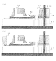
【選択図】図4A manufacturing method of a droplet discharge head, etc., capable of improving bonding accuracy.
An alignment pin hole of a cavity substrate having a vibration plate made of silicon and having a vibrating plate that pressurizes a liquid, and an alignment pin hole of at least one other substrate are provided in an alignment pin. In this method, the cavity substrate 20 and another substrate are joined together to form a liquid flow path, thereby forming a liquid discharge head, which is an alignment pin hole 62B of the silicon substrate 61 to be the cavity substrate 20. A step of covering the portion other than the portion to be covered with the silicon mask 64 and a step of forming the alignment pin hole 62B of the silicon substrate 61 by anisotropic dry etching.
[Selection] Figure 4
Description
本発明は液滴吐出ヘッドを製造する方法等に関するものである。特にその製造時におけるアライメントを高精度に行うためのものである。 The present invention relates to a method for manufacturing a droplet discharge head and the like. In particular, this is for performing alignment at the time of manufacture with high accuracy.
現在、液滴吐出方式の記録(印刷)装置は、家庭用、工業用を問わず、あらゆる分野の印刷に利用されている。液滴吐出方式とは、例えば複数のノズルを有する液滴吐出ヘッドを対象物(紙等)との間で相対移動させ、液滴吐出ヘッドから吐出した液滴を対象物の所定の位置に付着させて印刷等をするものである。この方式は、液晶(Liquid Crystal)を用いた表示装置を作製する際のカラーフィルタ、有機化合物等の電界発光(ElectroLuminescence )素子を用いた表示パネル(OLED)、DNA、タンパク質等、生体分子のマイクロアレイ等の製造にも利用されている。 Currently, a recording (printing) apparatus using a droplet discharge method is used for printing in various fields regardless of whether it is for home use or industrial use. In the droplet discharge method, for example, a droplet discharge head having a plurality of nozzles is moved relative to an object (paper, etc.), and the droplet discharged from the droplet discharge head is attached to a predetermined position of the object. Printing and so on. This method uses a color filter for manufacturing a display device using liquid crystal, a display panel using an electroluminescence element such as an organic compound (OLED), a microarray of biomolecules such as DNA and protein. Etc. are also used in the manufacture of
液滴吐出方式を実現する吐出ヘッドとして、吐出液体を溜めておく吐出室の少なくとも一面の壁(ここでは底壁とする。この壁は他の壁と一体形成されているが、以下、この壁のことを振動板ということにする)が撓んで形状が変化するようにしておき、振動板を撓ませて吐出室内の圧力を高め、吐出室と連通するノズルから液滴を吐出させるものがある。そして、このような液滴吐出ヘッドを製造する際の材料として、例えば、ガラス基板、シリコン基板が用いられる。そして、各基板に部材形成を行い、積層し、接合して製造をしている(例えば特許文献1参照)。
このような液滴吐出ヘッドに関し、近年、高精細な印刷等が要求されており、そのためにノズル、ノズルに連通する流路等の高密度化、吐出性能の向上が進んでいる。また、液滴吐出ヘッドの構造も複雑化しており、そのため、例えば流路を構成するために積層する基板の数も増えつつある。 In recent years, high-definition printing or the like has been demanded for such a droplet discharge head, and for this reason, the density of nozzles and flow paths communicating with the nozzles has been increased, and the discharge performance has been improved. In addition, the structure of the droplet discharge head is also complicated, and for this reason, for example, the number of substrates stacked to form a flow path is increasing.
以上のことから従来以上に積層する基板を接合する(貼り合わせる)精度を高める必要があるが、十分な精度が得られていないのが現状である。 From the above, it is necessary to increase the accuracy of bonding (bonding) the substrates to be laminated more than before, but at present, sufficient accuracy has not been obtained.
そこで、本発明はこのような問題を解決するため、アライメント精度をたかめ、接合(貼り合わせ)精度を高めることができるような液滴吐出ヘッドの製造方法等を得ることを目的とする。 Accordingly, an object of the present invention is to provide a manufacturing method of a droplet discharge head that can increase alignment accuracy and increase bonding (bonding) accuracy in order to solve such problems.
本発明に係る液滴吐出ヘッドの製造方法は、シリコンからなり、振動により液体を加圧する振動板を有するキャビティ基板のアライメントピン穴と、少なくとも1枚の他の基板のアライメントピン穴とを、アライメントピンに通した状態で、キャビティ基板と他の基板とを接合することによって、液体の流路を形成する液滴吐出ヘッドの製造方法であって、キャビティ基板となる基板のアライメントピン穴となる部分以外をマスクにより覆う工程と、キャビティ基板となる基板のアライメントピン穴を異方性ドライエッチングにより形成する工程とを有する。
本発明によれば、キャビティ基板となるシリコンの基板に形成するアライメントピン穴の部分以外をマスクにより覆い、アライメントピン穴を異方性ドライエッチングにより加工するようにしたので、キャビティ基板に形成する流路に対する位置精度を損なうことなくアライメントピン穴のみを選択的にエッチングすることができる。また、ドライエッチングを行うことにより、アライメントピン穴の形状の自由度を高くすることができるため、例えば円形のような強度が高く、ストレス耐性の高い形状にアライメントピン穴を開口することができ、アライメントピンを用いたアライメント(位置合わせ)、それに伴う基板の接合(貼り合わせ)を高精度で行うことができる。そのため、ノズルの高密度化に対応することができ、で吐出性能の高い液滴吐出ヘッドを製造することができる。
The manufacturing method of a droplet discharge head according to the present invention includes an alignment pin hole of a cavity substrate made of silicon and having a vibration plate that pressurizes a liquid by vibration, and an alignment pin hole of at least one other substrate. A method of manufacturing a droplet discharge head that forms a liquid flow path by bonding a cavity substrate and another substrate while being passed through a pin, and a portion that becomes an alignment pin hole of the substrate that becomes the cavity substrate And a step of forming an alignment pin hole of a substrate to be a cavity substrate by anisotropic dry etching.
According to the present invention, the portion other than the alignment pin hole formed in the silicon substrate serving as the cavity substrate is covered with the mask, and the alignment pin hole is processed by anisotropic dry etching. Only the alignment pin hole can be selectively etched without impairing the positional accuracy with respect to the path. Moreover, since the degree of freedom of the shape of the alignment pin hole can be increased by performing dry etching, the alignment pin hole can be opened in a shape having high strength such as a circle and high stress resistance, for example, Alignment (positioning) using alignment pins and accompanying substrate bonding (bonding) can be performed with high accuracy. Therefore, it is possible to cope with the high density of the nozzles, and it is possible to manufacture a droplet discharge head with high discharge performance.
また、本発明に係る液滴吐出ヘッドの製造方法は、アライメントピン穴を異方性ドライエッチングにより形成した後、キャビティ基板となる基板のアライメントピン穴をウェットエッチング液から保護するための処理を行う工程と、ウェットエッチングによって、キャビティ基板となる基板に流路の一部を形成する工程とをさらに有する。
本発明によれば、アライメントピン穴を形成した後、エッチング液からアライメントピン穴を保護するための処理を行ってから流路を形成するようにしたので、流路形成をアライメントピン穴形成より後の工程にすることで、流路を破損させずにすみ、ウェットエッチングを行うことで、高精度で生産性の高い流路形成を行うことができる。
In the method of manufacturing a droplet discharge head according to the present invention, after forming the alignment pin holes by anisotropic dry etching, a process for protecting the alignment pin holes of the substrate to be the cavity substrate from the wet etching solution is performed. And a step of forming a part of the flow path in the substrate to be the cavity substrate by wet etching.
According to the present invention, after the alignment pin hole is formed, the flow path is formed after the processing for protecting the alignment pin hole from the etching solution is performed. By using this process, it is possible to form the flow path with high accuracy and high productivity by performing wet etching without damaging the flow path.
また、本発明に係る液滴吐出ヘッドの製造方法は、キャビティ基板となる基板のアライメントピン穴をウェットエッチング液から保護するために、耐アルカリエッチング樹脂を用いる。
本発明によれば、耐アルカリエッチング樹脂によりアライメントピン穴を保護するようにしたので、シリコン基板をウェットエッチングする際のエッチング液(エッチャント)となるアルカリ溶液から適切にアライメントピン穴の形状を保護することができる。
In addition, the method for manufacturing a droplet discharge head according to the present invention uses an alkali-resistant etching resin in order to protect the alignment pin holes of the substrate serving as the cavity substrate from the wet etching solution.
According to the present invention, since the alignment pin hole is protected by the alkali-resistant etching resin, the shape of the alignment pin hole is appropriately protected from an alkaline solution that becomes an etching solution (etchant) when the silicon substrate is wet-etched. be able to.
また、本発明に係る液滴吐出ヘッドの製造方法は、振動板を振動させるための電極を有する電極基板とキャビティ基板となる基板とを接合した後、接合した面と反対側の面から、キャビティ基板となる基板のアライメントピン穴となる部分以外をマスクにより覆う。
本発明によれば、接合基板に対してアライメントピン穴を形成するようにしたので、電極基板との接合により基板を安定させた後に、アライメントピン穴を形成することができる。
Also, in the method for manufacturing a droplet discharge head according to the present invention, after joining an electrode substrate having an electrode for vibrating a diaphragm and a substrate to be a cavity substrate, a cavity is formed from a surface opposite to the joined surface. A portion other than the alignment pin hole of the substrate to be the substrate is covered with a mask.
According to the present invention, since the alignment pin hole is formed on the bonding substrate, the alignment pin hole can be formed after the substrate is stabilized by bonding with the electrode substrate.
また、本発明に係る液滴吐出装置の製造方法は、上記の液滴吐出ヘッドの製造方法を適用して液滴吐出装置を製造する。
本発明によれば、上記の液滴吐出ヘッドの製造方法により液滴吐出装置を製造するようにしたので、アライメント精度が高く、ノズルの高密度化にも適用することができ、高精細で吐出性能の高い液滴吐出装置を製造することができる。
The manufacturing method of the droplet discharge device according to the present invention applies the above-described manufacturing method of the droplet discharge head to manufacture the droplet discharge device.
According to the present invention, since the droplet discharge device is manufactured by the method of manufacturing the droplet discharge head described above, the alignment accuracy is high, and the method can be applied to increase the density of the nozzles. A high-performance droplet discharge device can be manufactured.
実施の形態1.
図1は本発明の実施の形態1に係る液滴吐出ヘッドを分解して表した図である。図1は液滴吐出ヘッドの一部を示している。また、図2は液滴吐出ヘッドの断面図を表す図である。本実施の形態では、例えば静電方式で駆動する静電アクチュエータを用いるデバイスとなるフェイスイジェクト型の液滴吐出ヘッドについて説明する。(なお、構成部材を図示し、見やすくするため、図1を含め、以下の図面では各構成部位(部材)の大きさの関係が実際のものと異なる場合がある。また、図における上側を上とし、下側を下として説明する)。
FIG. 1 is an exploded view of a droplet discharge head according to
図1に示すように本実施の形態に係る液滴吐出ヘッドは、電極基板10、キャビティ基板20、リザーバ基板30及びノズル基板40の4つの基板が下から順に積層されて構成される。ここで本実施の形態では、電極基板10とキャビティ基板20とは陽極接合により接合する。また、キャビティ基板20とリザーバ基板30、リザーバ基板30とノズル基板40とはエポキシ樹脂等の接着剤を用いて接合する。
As shown in FIG. 1, the droplet discharge head according to the present embodiment is configured by stacking four substrates in order from the bottom: an
第1の基板となる電極基板10は、厚さ約1mmの例えばホウ珪酸系の耐熱硬質ガラス等の基板を主要な材料としている。本実施形態では、ガラス基板とするが、例えば単結晶シリコンを基板とすることもできる。電極基板10の表面には、後述するキャビティ基板20に形成される吐出室21となる凹部に合わせて、例えば深さ約0.3μmを有する複数の凹部11が形成されている。また、キャビティ基板20の各吐出室21(振動板22)と対向する凹部11の内側(特に底部)には、固定電極となる個別電極12が設けられている。個別電極12は電極部、リード部及び端子部を有し、端子部を介してICドライバ50と電気的に接続され、ICドライバ50から電圧印加(電荷供給)等が行われる。この個別電極12は、例えばスパッタ法により、ITO(Indium Tin Oxide:インジウム錫酸化物)を0.1μmの厚さで凹部11の内側に成膜することで形成される。そして、振動板22と個別電極12との間は、凹部11により振動板22が撓む(変位する)ことができる一定のギャップ(凹部11等に囲まれた空間、空隙室)が形成される。
The
さらに、凹部11には、後述するFPC51からICドライバ50に各個別電極12にそれぞれ個別の電荷供給制御を行うためのSEG信号を送信するためのリード線(配線)の役割を果たす信号リード線13が設けられている、ICドライバ50が収容されたときに、ICドライバ50の直下となる部分に配される。また、電極基板10には、他にも外部のタンク(図示せず)から供給された液体を取り入れる流路となる液体取り入れ口14となる貫通穴が設けられている。
Further, in the recess 11, a
キャビティ基板20は、シリコン単結晶基板(以下、シリコン基板という)を主要な材料としている。本実施の形態では、例えば厚さ約50μmで表面が(110)面方位のシリコン基板であるものとする。キャビティ基板20には、吐出室21となる凹部(底壁がボロンドープ層で形成され、可動電極となる振動板22となっている)が形成されている。また、キャビティ基板20の下面(電極基板10と対向する面)には、振動板22と個別電極12との間を電気的に絶縁するための絶縁膜23が成膜されている。絶縁膜23は、例えばプラズマCVD(Chemical Vapor Deposition :TEOS−pCVDともいう)法を用いて、0.1μmのTEOS膜により成膜する。ここでは絶縁膜23をTEOS膜としているが、例えばAl2O3(酸化アルミニウム(アルミナ))を用いてもよい。さらに、キャビティ基板20にも液体取り入れ口14となる貫通穴が設けられている(電極基板10に設けられた貫通穴と連通する)。さらに、外部の電力供給手段(図示せず)から基板(振動板22)に個別電極12と反対の極性の電荷を供給する際の端子となる共通電極端子25を備えている。また、ICドライバを収容するためのドライバ収容部26となる貫通穴を有している。
The
リザーバ基板30は例えばシリコン基板を主要な材料とする。リザーバ基板30には、各吐出室21に液体を供給するリザーバ(共通液室)31となる凹部が形成されている。この凹部の底面にも、液体取り入れ口14となる貫通穴(電極基板10に設けられた貫通穴と連通する)が設けられている。また、凹部の底面には、リザーバ31から各吐出室21に液体を供給するための供給口32が各吐出室21の位置に合わせて形成されている。そして、各吐出室21とノズル基板40に設けられたノズル41との間の流路となり、吐出室21で加圧された液体がノズル41に移送する流路となる複数のノズル連通孔33が各ノズル(各吐出室21)に合わせて設けられている。また、ICドライバ50を収容するためのドライバ収容部26となる貫通穴(キャビティ基板20に設けられた貫通穴と連通する)を有している。
The
ノズル基板40についても、例えばシリコン基板を主要な材料とする。ノズル基板40には、複数のノズル41が形成されている。各ノズル41は、各ノズル連通孔33から移送された液体を液滴として外部に吐出する。本実施の形態のノズル基板40は、2段で形成されたノズル41を複数有しているものとする。ノズル41を複数段で形成すると、液滴を吐出する際の直進性向上が期待できる。ここで、振動板22によりリザーバ31側の液体に加わる圧力を緩衝するためのダイヤフラムを設けるようにしてもよい。ここで、ノズル基板40が蓋となって、ドライバ収容部26に収容したICドライバ50が保護される。
For the
ICドライバ50は、液滴吐出ヘッドにある複数の個別電極12に対して、それぞれ独立して電圧を印加し、電荷供給、維持、放電等を行うための手段である。本実施の形態では、2つのICドライバ50を収容するようにしているが、この数について限定するものではない。また、FPC(Flexible Print Circuit)51は、駆動制御手段(図示せず)からの信号を液滴吐出ヘッド側に送信するための配線が設けられている。配線は、共通電極端子25を介して液滴吐出ヘッド内の全振動板22に対して共通した電荷供給制御を行うためのCOM信号を送信するFPC配線51a及び信号リード線13を介してICドライバ50に前述したSEG信号を送信するFPC配線51bからなる。
The
図2は液滴吐出ヘッドの断面図である。振動板22と個別電極12との間に形成されたギャップ(空間、空隙)は、封止材24による封止により、ドライバ収容部26の空間と連通することなく、外気と遮断されている。
FIG. 2 is a cross-sectional view of the droplet discharge head. A gap (space, space) formed between the
例えば、ドライバIC50に選択された個別電極12には約40Vの電圧が印可され、正に帯電する。このとき、振動板22は相対的に負に帯電する(ここでは、FPC(Flexible Print Circuit)等、共通電極端子25を介してキャビティ基板20には負の極性を有する電荷が供給される)。そのため、選択された個別電極12と振動板22との間では静電気力が発生し、個別電極12に引き寄せられて撓む。これにより吐出室21の容積は広がる。そして電荷供給を止めると振動板22は元に戻ろうとする。そのとき吐出室21の容積も元に戻り、その圧力で加圧された液体がノズル41から液滴として吐出する。この液滴が例えば記録紙に着弾することによって印刷等が行われる。
For example, a voltage of about 40 V is applied to the individual electrode 12 selected by the
前述のように、本実施の形態の液滴吐出ヘッドは、流路等となる凹部等を形成する加工を施した4枚の基板を積層して構成し、ノズルに至るまでの流路を形成している。高密度に形成された凹部を、対応するノズルに合わせて積層して接合(貼り合わせる)ためには、高精度の位置合わせ(アライメント)を行う必要がある。基板のアライメント方法については、例えば基板(ウェハ)にアライメントピン穴を形成し、アライメントピンに差し入れる方法がある。ここで、シリコン基板の加工(特にキャビティ基板20を作製するための加工)では異方性ウェットエッチング(以下、ウェットエッチングという)により行うことが多く、アライメントピン穴はその加工時のウェットエッチングにより形成することが一般的である。 As described above, the droplet discharge head according to the present embodiment is formed by stacking four substrates that have been processed to form recesses or the like that serve as flow paths, and forms a flow path that leads to the nozzle. is doing. In order to stack the concave portions formed at a high density in accordance with the corresponding nozzles and bond (bond), it is necessary to perform alignment (alignment) with high accuracy. As a substrate alignment method, for example, there is a method of forming an alignment pin hole in a substrate (wafer) and inserting it into the alignment pin. Here, the processing of the silicon substrate (especially processing for manufacturing the cavity substrate 20) is often performed by anisotropic wet etching (hereinafter referred to as wet etching), and the alignment pin hole is formed by wet etching at the time of processing. It is common to do.
ただ、例えばウェットエッチングでは、表面が(110)面方位のシリコン基板に形成できるアライメントピン穴は円形状とはならず、いびつな形状となる。そのため、アライメントピン穴の一部のみがアライメントピンと接することでシリコン基板(キャビティ基板20)が固定されることになる。このとき、過度の負荷(ストレス)がアライメントピン穴の一部にかかり、チッピング(欠損による微小粒子の発生)、基板の破損等を招くおそれがある。また、このようなチッピング等により、アライメントピンとうまく接しなくなり、貼り合わせ位置がずれることもある。 However, in wet etching, for example, alignment pin holes that can be formed on a silicon substrate having a (110) surface orientation are not circular but distorted. Therefore, the silicon substrate (cavity substrate 20) is fixed by only a part of the alignment pin hole coming into contact with the alignment pin. At this time, an excessive load (stress) is applied to a part of the alignment pin hole, which may cause chipping (generation of fine particles due to defects), damage to the substrate, and the like. Further, due to such chipping or the like, it may not be in good contact with the alignment pin, and the bonding position may be shifted.
そこで、本実施の形態では、位置合わせを行うためのアライメントピンを通すアライメントピン穴の形状の自由度を確保するために、アライメントピン穴を異方性ドライエッチング(以下、ドライエッチングという)を行って形成するようにする。例えば、アライメントピン穴をストレス耐性の高い円形状に形成し、アライメントピン穴全体がアライメントピンと接するようにして、チッピング、破損等を防止してアライメント精度を高める。また、流路等をシリコン基板に加工するためのウェットエッチングを行う前に、形成したアライメントピン穴をウェットエッチングから保護するための処理を行う。 Therefore, in this embodiment, the alignment pin hole is subjected to anisotropic dry etching (hereinafter referred to as dry etching) in order to ensure the degree of freedom of the shape of the alignment pin hole through which the alignment pin for alignment is passed. To form. For example, the alignment pin hole is formed in a circular shape having high stress resistance, and the entire alignment pin hole is in contact with the alignment pin to prevent chipping, breakage, and the like, thereby improving alignment accuracy. In addition, before the wet etching for processing the flow path and the like into the silicon substrate, a process for protecting the formed alignment pin hole from the wet etching is performed.
図3、図4及び図5は本実施の形態に係る電極基板10及びキャビティ基板20の製造工程を表す図である。図3〜図5に基づいて液滴吐出ヘッドにおける電極基板10及びキャビティ基板20の製造について説明する。なお、ここではウェハ単位で複数個分の液滴吐出ヘッドの部位等を同時形成するが、図5〜図7ではその一部分だけを示している。
3, 4, and 5 are diagrams illustrating manufacturing steps of the
シリコン基板61の片面(電極基板10との接合面側となる)を鏡面研磨し、例えば220μmの厚さの基板(キャビティ基板20となる)を作製する。次に、シリコン基板61のボロンドープ層を形成する面を、B2O3を主成分とする固体の拡散源に対向させて石英ボートにセットする。さらに縦型炉に石英ボートをセットして、炉内を窒素雰囲気にし、温度を1050℃に上昇させて7時間保持することで、ボロンをシリコン基板61中に拡散させ、ボロンドープ層(図示せず)を形成する。取り出したボロンドープ層の表面にはボロン化合物(SiB6 :ケイ化6ホウ素)が形成されているが(図示せず)、酸素及び水蒸気雰囲気中、600℃の条件で1時間30分酸化させると、フッ酸水溶液によるエッチングが可能なB2O3+SiO2 に化学変化させることができる。B2O3+SiO2 に化学変化させた状態で、B2O3+SiO2 を、フッ酸水溶液にて異方性ウェットエッチング(以下、ウェットエッチングという)して除去する。ボロンドープ層を形成した面に、プラズマCVD法により、成膜時の処理温度は360℃、高周波出力は250W、圧力は66.7Pa(0.5Torr)、ガス流量はTEOS流量100cm3 /min(100sccm)、酸素流量1000cm3 /min(1000sccm)の条件で例えば、絶縁膜23を0.1μm成膜する(図3(a))。そして、液体取り入れ口14となる部分の絶縁膜23を除去する(図3(b))。
One side of the silicon substrate 61 (becomes the bonding surface side with the electrode substrate 10) is mirror-polished to produce, for example, a 220 μm thick substrate (becomes the cavity substrate 20). Next, the surface of the silicon substrate 61 on which the boron doped layer is to be formed is set on a quartz boat so as to face a solid diffusion source containing B 2 O 3 as a main component. Further, a quartz boat is set in a vertical furnace, the inside of the furnace is put into a nitrogen atmosphere, the temperature is raised to 1050 ° C. and held for 7 hours, whereby boron is diffused into the silicon substrate 61 and a boron doped layer (not shown) ). A boron compound (SiB 6 : 6 boron silicide) is formed on the surface of the boron doped layer taken out (not shown), but when oxidized in an oxygen and water vapor atmosphere at 600 ° C. for 1 hour and 30 minutes, It can be chemically changed to B 2 O 3 + SiO 2 which can be etched with a hydrofluoric acid aqueous solution. B 2 O 3 + SiO 2 is removed by anisotropic wet etching (hereinafter referred to as wet etching) with a hydrofluoric acid aqueous solution in a state of being chemically changed to B 2 O 3 + SiO 2 . On the surface on which the boron doped layer is formed, the processing temperature during film formation is 360 ° C., the high frequency output is 250 W, the pressure is 66.7 Pa (0.5 Torr), and the gas flow rate is TEOS flow rate 100 cm 3 / min (100 sccm). For example, the insulating
電極基板10については、上記図3(a)、(b)とは別工程で作製する。約1mmのガラスの基板の一方の面に対し、約0.3μmの深さの凹部11を形成する。凹部11の形成後、例えばスパッタリング法を用いて、0.1μmの厚さの個別電極12、リード線13を同時に形成する。最後に液体取り入れ口14及び電極基板用アライメントピン穴62Aとなる穴をサンドブラスト法または切削加工等により所定の形状で形成する。これにより、電極基板10を作製する。そして、シリコン基板61と電極基板10を360℃に加熱した後、電極基板10に負極、シリコン基板61に正極を接続して、800Vの電圧を印加して陽極接合を行う(図3(c))。ここで、電極基板用アライメントピン穴62Aについては、ウェハ上に2つ形成しておけば、アライメントピンにより基板を固定することができる。そのため、本実施の形態では例えば、ウェハ中心を点対称とする基板端の2点に電極基板用アライメントピン穴62Aを形成する。ただ、これに限定するものではない。例えば予備用として、別の箇所に電極基板用アライメントピン穴62Aを設けるようにしてもよい。これは、以下に示す各基板のアライメントピン穴についても同様である。
The
陽極接合後の接合済み基板(以下、接合済み基板という)に対し、シリコン基板61の厚さが例えば約60μmになるまでシリコン基板61表面の研削(研磨)加工を行って薄板化を行う。その後、加工変質層を除去する為に、32w%の濃度の水酸化カリウム溶液により、シリコン基板61に対して約10μmのウェットエッチングを行う。これによりシリコン基板61の厚さを約50μmにする(図3(d))。 The bonded substrate after anodic bonding (hereinafter referred to as bonded substrate) is thinned by grinding (polishing) the surface of the silicon substrate 61 until the thickness of the silicon substrate 61 becomes, for example, about 60 μm. Thereafter, in order to remove the work-affected layer, the silicon substrate 61 is wet-etched with a potassium hydroxide solution having a concentration of 32 w%. As a result, the thickness of the silicon substrate 61 is reduced to about 50 μm (FIG. 3D).
次に、ウェットエッチングを行った面に対し、TEOSによる酸化シリコンのハードマスク(以下、TEOSハードマスクという)63をプラズマCVD法により成膜する(図3(e))。成膜条件としては、例えば、成膜時の処理温度は360℃、高周波出力は700W、圧力は33.3Pa(0.25Torr)、ガス流量はTEOS流量100cm3 /min(100sccm)、酸素流量1000cm3 /min(1000sccm)の条件で1.5μm成膜する。TEOSを用いた成膜は比較的低温で行うことができ、基板の加熱をできる限り抑えられる点で都合がよい。 Next, a silicon oxide hard mask (hereinafter referred to as TEOS hard mask) 63 made of TEOS is formed on the wet-etched surface by plasma CVD (FIG. 3E). As film formation conditions, for example, the processing temperature during film formation is 360 ° C., the high-frequency output is 700 W, the pressure is 33.3 Pa (0.25 Torr), the gas flow rate is TEOS flow rate 100 cm 3 / min (100 sccm), and the oxygen flow rate is 1000 cm. A film having a thickness of 1.5 μm is formed under the condition of 3 / min (1000 sccm). Film formation using TEOS can be performed at a relatively low temperature, which is advantageous in that heating of the substrate can be suppressed as much as possible.
TEOSハードマスク63を成膜した後、吐出室21、ドライバ収容部26、液体取り入れ口14、キャビティ基板用アライメントピン穴62B(貫通穴)となる部分のTEOSハードマスク63をエッチングするため、レジストパターニングを施す。そして、フッ酸水溶液を用いてTEOSハードマスク63が無くなるまで、それらの部分をエッチングしてTEOSハードマスク63をパターニングし、それらの部分について、シリコン基板61を露出させる。エッチングした後にレジストを剥離する(図3(f))。
After the TEOS hard mask 63 is formed, resist patterning is performed in order to etch the TEOS hard mask 63 in the
次に、キャビティ基板用アライメントピン穴62Bとなる部分を貫通させたシリコンマスク64をシリコン基板61側から接合済み基板に載置する。そして、例えばICP(Inductively Coupled Plasma)ドライエッチングを行い、キャビティ基板用アライメントピン穴62Bを形成する(図4(g))。ICPドライエッチングを行う条件について、エッチングプロセスにおいては、SF6 流量400cm3 /min(400sccm)、エッチング時間3.5秒、チャンバー圧力8Pa、コイルパワー2200W、プラテンパワー55W、プラテン温度20℃とする。また、デポジションプロセスにおいては、C4F8流量200cm3 /min(200sccm)、エッチング時間2.5秒、チャンバー圧力2.7Pa、コイルパワー1800W、プラテン温度20℃とする。そして、エッチングプロセスとデポジションプロセスとを組み合わせて1サイクルとし、約150サイクル行って、キャビティ基板用アライメントピン穴62Bとなる部分のシリコン基板61を所定の形状で貫通させる。ここでは、基板表面に対して垂直方向にエッチングするのに適したICPドライエッチングとするが特に限定するものではない。 Next, a silicon mask 64 penetrating through the portion serving as the cavity substrate alignment pin hole 62B is placed on the bonded substrate from the silicon substrate 61 side. Then, for example, ICP (Inductively Coupled Plasma) dry etching is performed to form the cavity substrate alignment pin hole 62B (FIG. 4G). Regarding the conditions for ICP dry etching, in the etching process, the SF 6 flow rate is 400 cm 3 / min (400 sccm), the etching time is 3.5 seconds, the chamber pressure is 8 Pa, the coil power is 2200 W, the platen power is 55 W, and the platen temperature is 20 ° C. In the deposition process, the C 4 F 8 flow rate is 200 cm 3 / min (200 sccm), the etching time is 2.5 seconds, the chamber pressure is 2.7 Pa, the coil power is 1800 W, and the platen temperature is 20 ° C. Then, the etching process and the deposition process are combined into one cycle, and about 150 cycles are performed to penetrate the silicon substrate 61 in a predetermined shape to become the cavity substrate alignment pin hole 62B. Here, ICP dry etching suitable for etching in a direction perpendicular to the substrate surface is used, but there is no particular limitation.
ここで、本実施の形態ではキャビティ基板用アライメントピン穴62Bを形成してから、ウェットエッチングにより吐出室21等の液体の流路を形成する。これは、例えば形成した流路に係る部分(特に振動板22)が薄くて脆くなるため、例えばキャビティ基板用アライメントピン穴62Bを形成する際に、破損する可能性が高くなるからである。そのため、ウェットエッチングの工程よりも先にキャビティ基板用アライメントピン穴62Bを形成する。
In this embodiment, after the cavity substrate alignment pin hole 62B is formed, a liquid flow path such as the
このような関係で、後に行うウェットエッチングの工程において、所定の形状で形成したキャビティ基板用アライメントピン穴62Bがエッチングされて変形しないように、アルカリエッチング用の保護膜となる耐アルカリエッチング樹脂65をポッティングして封止する(図4(h))。ここでは電極基板用アライメントピン穴62Aの部分についてもポッティングし、封止している。耐アルカリエッチング樹脂65としては、例えばジエチレングリコールジメチルエーテル、5−メチル−2−ヘキサノンを含むポリマー樹脂がある。 In such a relationship, in the subsequent wet etching process, the alkali etching resistant resin 65 serving as a protective film for alkaline etching is used so that the cavity substrate alignment pin hole 62B formed in a predetermined shape is not etched and deformed. Potting and sealing are performed (FIG. 4 (h)). Here, the electrode substrate alignment pin hole 62A is also potted and sealed. Examples of the alkali-resistant etching resin 65 include polymer resins containing diethylene glycol dimethyl ether and 5-methyl-2-hexanone.
次に、接合済み基板を35wt%の濃度の水酸化カリウム(KOH)水溶液に浸し、吐出室21、ドライバ収容部26、液体取り入れ口14となる部分の厚さが約10μmになるまでウェットエッチングを行う。さらに、接合済み基板を3wt%の濃度の水酸化カリウム水溶液に浸し、ボロンドープ層が露出し、エッチングの進行が極度に遅くなるエッチングストップが十分効いたものと判断するまでウェットエッチングを続ける(図4(i))。このように、前記2種類の濃度の異なる水酸化カリウム水溶液を用いたエッチングを行うことによって、吐出室21となる部分に形成される振動板22の面荒れを抑制し、厚さ精度を0.80±0.05μm以下にすることができる。その結果、液滴吐出ヘッドの吐出性能を安定化することができる。
Next, the bonded substrate is dipped in a 35 wt% potassium hydroxide (KOH) aqueous solution, and wet etching is performed until the thicknesses of the
ウェットエッチングを終了すると、接合済み基板を有機溶剤中に浸して耐アルカリエッチング樹脂65を除去する(図4(j))。この有機溶剤としては、例えば5−メチル−2−ヘキサノンを含む有機溶剤がある。 When the wet etching is completed, the bonded substrate is immersed in an organic solvent to remove the alkali-resistant etching resin 65 (FIG. 4 (j)). Examples of the organic solvent include an organic solvent containing 5-methyl-2-hexanone.
ドライバ収容部26、液体取り入れ口14となる部分のボロンドープ層を除去するため、ドライバ収容部26となる部分が開口したシリコンマスク66を、接合済み基板のシリコン基板61側の表面に取り付ける。そして、例えば、RFパワー200W、圧力40Pa(0.3Torr)、CF4 流量30cm3 /min(30sccm)の条件で、RIEドライエッチング(異方性ドライエッチング)を30分間行い、ドライバ収容部26、液体取り入れ口14となる部分にプラズマを当てて、開口する(図4(k))。ここで、例えば接合済み基板とシリコンマスク66とのアライメント精度を高めるため、シリコンマスク66の装着は、接合済み基板とシリコンマスク66とをアライメントピン67に通して行うようにするとよい。
In order to remove the boron doped layer in the portion that becomes the
さらに共通電極端子25となる部分を開口したマスク68を、接合済み基板のシリコン基板61側の表面に取り付ける。そして、共通電極端子25となる部分のTEOSハードマスク63を除去した後(図5(l))、さらに、例えばプラチナ(Pt)をターゲットとしてスパッタ等を行い、共通電極端子25を形成する(図5(m))。このときも、接合済み基板とマスク68とをアライメントピン67に通して行うようにするとよい。
Further, a mask 68 having an opening at the portion to be the
さらに、例えば、ギャップへの水分透過等を防ぐために、TEOSを用いたプラズマCVD、蒸着、スパッタ等により、封止材24を堆積させて封止を行う(図5(n))。堆積させる封止材24の厚さについては、特に限定しないが、ギャップの幅が約0.2μmであることから、例えば最薄部分で約2〜3μm又はそれ以上、他の基板との接合に影響しない範囲で堆積できればよい。以上のようにして、キャビティ基板20の作製等を行い、キャビティ基板20と電極基板10とが接合された接合済み基板を作製する。
Further, for example, in order to prevent moisture permeation through the gap, sealing is performed by depositing the sealing
図6及び図7はリザーバ基板30及びノズル基板40接合等に係る工程を表す図である。接合済み基板を例えば前述したアライメントピン67に通す。そして、あらかじめ別工程で作製していたリザーバ基板30を、例えばエポキシ系接着剤により、接合済み基板のキャビティ基板20側から接着し、接合する(図6(a))。ここで、リザーバ基板30についても、リザーバ31となる凹部等を形成する際に、ウェットエッチングを行うため、リザーバ基板30となるシリコン基板に対し、例えばICPドライエッチングによるリザーバ基板用アライメントピン穴62Cを形成しておく。ここで、リザーバ基板31となるシリコン基板にリザーバ31となる凹部等を形成する際にもウェットエッチングを行うため、前述したように耐アルカリエッチング樹脂によりリザーバ基板用アライメントピン穴62Cを保護する。ウェットエッチングが終了すると、有機溶剤により耐アルカリエッチング樹脂を除去するようにする。また、ドライバIC50を個別電極12等と接続する(図6(b))。
6 and 7 are diagrams showing processes related to bonding of the
さらに別工程で作製していたノズル基板40についても同様に、例えばエポキシ系接着剤により、接合したリザーバ基板30側から接着し、接合する(図7(c))。ノズル基板40についても、ノズル41を形成する際に例えばICPドライエッチングによるノズル基板用アライメントピン穴62Dを形成しておく。そして、ダイシングラインに沿ってダイシングを行い、個々のチップに切断し、液滴吐出ヘッドが完成する(図7(d))。このとき、アライメントピン穴の部分はダイシングにより、基本的には液滴吐出ヘッドには残らない。
Further, the
以上のように実施の形態1によれば、キャビティ基板20におけるキャビティ基板用アライメントピン穴62Bの形成をICPドライエッチング等の異方性ドライエッチングにより行うようにしたので、所定の形状でアライメントピン穴を形成することができる。そのため、チッピング、基板の破損等を防ぎ、積層する他の基板(リザーバ基板30、ノズル基板40)と精度の高い貼り合わせを実現することができる。
As described above, according to the first embodiment, since the cavity substrate alignment pin hole 62B in the
実施の形態2.
前述の実施の形態では、4つの基板を積層して構成する液滴吐出ヘッドについて説明したが、積層する基板の数を4つに限定するものではない。例えば3層の液滴吐出ヘッドについても適用することができる。
In the above-described embodiment, the droplet discharge head configured by stacking four substrates has been described. However, the number of substrates stacked is not limited to four. For example, the present invention can also be applied to a three-layer droplet discharge head.
また、上述の実施の形態では、ウェハ単位でアライメント及び接合を行ったが、例えば先にダイシングした後、各液滴吐出ヘッド単位でアライメント及び接合を行うことができる。この場合には、各基板のアライメントピン穴は、液滴吐出ヘッド単位で形成するようにする。 In the above-described embodiment, alignment and bonding are performed in units of wafers. However, for example, after dicing first, alignment and bonding can be performed in units of each droplet discharge head. In this case, the alignment pin hole of each substrate is formed for each droplet discharge head.
実施の形態3.
図8は上述の実施の形態で製造した液滴吐出ヘッドを用いた液滴吐出装置(プリンタ100)の外観図である。また、図9は液滴吐出装置の主要な構成手段の一例を表す図である。図8及び図9の液滴吐出装置は液滴吐出方式(インクジェット方式)による印刷を目的とする。また、いわゆるシリアル型の装置である。図9において、被印刷物であるプリント紙110が支持されるドラム101と、プリント紙110にインクを吐出し、記録を行う液滴吐出ヘッド102とで主に構成される。また、図示していないが、液滴吐出ヘッド102にインクを供給するためのインク供給手段がある。プリント紙110は、ドラム101の軸方向に平行に設けられた紙圧着ローラ103により、ドラム101に圧着して保持される。そして、送りネジ104がドラム101の軸方向に平行に設けられ、液滴吐出ヘッド102が保持されている。送りネジ104が回転することによって液滴吐出ヘッド102がドラム101の軸方向に移動するようになっている。
FIG. 8 is an external view of a droplet discharge apparatus (printer 100) using the droplet discharge head manufactured in the above embodiment. FIG. 9 is a diagram illustrating an example of main constituent means of the droplet discharge device. 8 and 9 is intended for printing by a droplet discharge method (inkjet method). Further, it is a so-called serial type device. In FIG. 9, a drum 101 that supports a printing paper 110 that is a substrate to be printed and a
一方、ドラム101は、ベルト105等を介してモータ106により回転駆動される。また、プリント制御手段107は、印画データ及び制御信号に基づいて送りネジ104、モータ106を駆動させ、また、ここでは図示していないが、発振駆動回路を駆動させて振動板4を振動させ、制御をしながらプリント紙110に印刷を行わせる。
On the other hand, the drum 101 is rotationally driven by a motor 106 via a belt 105 or the like. Further, the
ここでは液体をインクとしてプリント紙110に吐出するようにしているが、液滴吐出ヘッドから吐出する液体はインクに限定されない。例えば、カラーフィルタとなる基板に吐出させる用途においては、カラーフィルタ用の顔料を含む液体、有機化合物等の電界発光素子を用いた表示パネル(OLED等)の基板に吐出させる用途においては、発光素子となる化合物を含む液体、基板上に配線する用途においては、例えば導電性金属を含む液体を、それぞれの装置において設けられた液滴吐出ヘッドから吐出させるようにしてもよい。また、液滴吐出ヘッドをディスペンサとし、生体分子のマイクロアレイとなる基板に吐出する用途に用いる場合では、DNA(Deoxyribo Nucleic Acids :デオキシリボ核酸)、他の核酸(例えば、Ribo Nucleic Acid:リボ核酸、Peptide Nucleic Acids:ペプチド核酸等)タンパク質等のプローブを含む液体を吐出させるようにしてもよい。その他、布等の染料の吐出等にも利用することができる。 Here, the liquid is ejected onto the print paper 110 as ink, but the liquid ejected from the droplet ejection head is not limited to ink. For example, in an application to be discharged onto a substrate to be a color filter, a light emitting element is used in an application to be discharged onto a substrate of a display panel (OLED or the like) using an electroluminescent element such as a liquid containing a color filter pigment or an organic compound. For example, a liquid containing a conductive metal and a liquid containing a conductive metal may be discharged from a droplet discharge head provided in each device. In addition, when the droplet discharge head is used as a dispenser and used for discharging onto a substrate that is a microarray of biomolecules, DNA (Deoxyribo Nucleic Acids: deoxyribonucleic acid), other nucleic acids (for example, Ribo Nucleic Acid: ribonucleic acid, Peptide (Nucleic Acids: peptide nucleic acids, etc.) A liquid containing a probe such as a protein may be discharged. In addition, it can also be used for discharging dyes such as cloth.
上述した実施の形態では、キャビティ基板となるシリコン基板について、アライメントピン穴となる部分をマスクで覆った後、ドライエッチングで加工する方法について説明した。ただ、特にキャビティ基板における作製の際に限定するものではなく、液滴吐出ヘッド製造の工程において、他のシリコン基板を加工する際に、上記の実施の形態のような方法を用いることができる。また、液滴吐出ヘッドだけでなく、他の加工素子においても適用することができる。 In the above-described embodiment, the method of processing the silicon substrate serving as the cavity substrate by dry etching after covering the portion serving as the alignment pin hole with the mask has been described. However, the present invention is not particularly limited to the fabrication on the cavity substrate, and the method described in the above embodiment can be used when processing another silicon substrate in the process of manufacturing the droplet discharge head. Further, it can be applied not only to the droplet discharge head but also to other processing elements.
1 液滴吐出ヘッド、10 電極基板、11 凹部、12 個別電極、12a ギャップ、13 信号リード線、14 液体取り入れ口、20 キャビティ基板、21 吐出室、22 振動板、23 絶縁膜、24 封止材、25 共通電極端子、26 ドライバ収容部、30 リザーバ基板、31 リザーバ、32 供給口、33 ノズル連通孔、40 ノズル基板、41 ノズル、50 ドライバIC、51 FPC 51a,51b FPC配線、61 シリコン基板、62A 電極基板用アライメントピン穴、62B キャビティ基板用アライメントピン穴、62C リザーバ基板用アライメントピン穴、62D ノズル基板用アライメントピン穴、63 TEOSハードマスク、64 シリコンマスク、65 耐アルカリエッチング樹脂、66 シリコンマスク、67 アライメントピン、68 マスク、100 プリンタ、101 ドラム、102 液滴吐出ヘッド、103 紙圧着ローラ、104 送りネジ、105 ベルト、106 モータ、107 プリント制御手段、110 プリント紙。
DESCRIPTION OF
Claims (5)
前記キャビティ基板となる基板のアライメントピン穴となる部分以外をマスクにより覆う工程と、
前記キャビティ基板となる基板のアライメントピン穴を異方性ドライエッチングにより形成する工程と
を有することを特徴とする液滴吐出ヘッドの製造方法。 An alignment pin hole of a cavity substrate made of silicon and having a vibration plate that pressurizes liquid by vibration and an alignment pin hole of at least one other substrate are passed through the alignment pin, and the cavity substrate and the other A droplet discharge head manufacturing method for forming the liquid flow path by bonding the substrate to the substrate,
A step of covering with a mask other than the portion serving as the alignment pin hole of the substrate to be the cavity substrate;
And a step of forming an alignment pin hole of the substrate to be the cavity substrate by anisotropic dry etching.
ウェットエッチングによって、前記キャビティ基板となる基板に前記流路の一部を形成する工程と
をさらに有することを特徴とする請求項1記載の液滴吐出ヘッドの製造方法。 After forming the alignment pin hole by anisotropic dry etching, performing a process for protecting the alignment pin hole of the substrate to be the cavity substrate from a wet etching solution;
The method of manufacturing a droplet discharge head according to claim 1, further comprising a step of forming a part of the flow path on the substrate to be the cavity substrate by wet etching.
Priority Applications (1)
| Application Number | Priority Date | Filing Date | Title |
|---|---|---|---|
| JP2007325594A JP2009143199A (en) | 2007-12-18 | 2007-12-18 | Droplet discharge head and method for manufacturing droplet discharge apparatus |
Applications Claiming Priority (1)
| Application Number | Priority Date | Filing Date | Title |
|---|---|---|---|
| JP2007325594A JP2009143199A (en) | 2007-12-18 | 2007-12-18 | Droplet discharge head and method for manufacturing droplet discharge apparatus |
Publications (1)
| Publication Number | Publication Date |
|---|---|
| JP2009143199A true JP2009143199A (en) | 2009-07-02 |
Family
ID=40914392
Family Applications (1)
| Application Number | Title | Priority Date | Filing Date |
|---|---|---|---|
| JP2007325594A Withdrawn JP2009143199A (en) | 2007-12-18 | 2007-12-18 | Droplet discharge head and method for manufacturing droplet discharge apparatus |
Country Status (1)
| Country | Link |
|---|---|
| JP (1) | JP2009143199A (en) |
Cited By (1)
| Publication number | Priority date | Publication date | Assignee | Title |
|---|---|---|---|---|
| JP2014113808A (en) * | 2012-12-12 | 2014-06-26 | Toshiba Corp | Ink jet head and ink jet head manufacturing method |
-
2007
- 2007-12-18 JP JP2007325594A patent/JP2009143199A/en not_active Withdrawn
Cited By (1)
| Publication number | Priority date | Publication date | Assignee | Title |
|---|---|---|---|---|
| JP2014113808A (en) * | 2012-12-12 | 2014-06-26 | Toshiba Corp | Ink jet head and ink jet head manufacturing method |
Similar Documents
| Publication | Publication Date | Title |
|---|---|---|
| JP4506717B2 (en) | Droplet discharge head and droplet discharge apparatus | |
| JP4259509B2 (en) | Electrostatic actuator, droplet discharge head, droplet discharge apparatus, electrostatic device, and manufacturing method thereof | |
| JP5315975B2 (en) | Nozzle substrate, droplet discharge head, droplet discharge apparatus, and manufacturing method thereof | |
| CN101007461A (en) | Electrostatic actuator, liquid droplet ejection head, liquid droplet ejection device and electrostatic driving device as well as methods of manufacturing them | |
| US20080057732A1 (en) | Method for manufacturing silicon substrate, method for manufacturing droplet discharging head, and method for manufacturing droplet discharging apparatus | |
| JP5612819B2 (en) | Nozzle substrate, droplet discharge head, and manufacturing method of droplet discharge apparatus | |
| JP2009143199A (en) | Droplet discharge head and method for manufacturing droplet discharge apparatus | |
| JP2007111957A (en) | Droplet discharge head, manufacturing method thereof, and droplet discharge apparatus | |
| CN100420575C (en) | Electrostatic actuator, liquid drop ejection head, liquid drop ejection device, and electrostatic device | |
| JP2009119699A (en) | MASK SUBSTRATE, MANUFACTURING METHOD THEREOF, AND LIQUID DISCHARGE EJECTING HEAD | |
| JP2007112075A (en) | Electrostatic actuator, droplet discharge head, droplet discharge apparatus, and electrostatic device manufacturing method | |
| JP2008093941A (en) | Nozzle substrate, droplet discharge head, method of manufacturing droplet discharge device, droplet discharge head, and droplet discharge device | |
| JP2008279707A (en) | Nozzle substrate, droplet discharge head, and manufacturing method of droplet discharge apparatus | |
| JP2008132646A (en) | Droplet discharge head and method for manufacturing droplet discharge apparatus | |
| JP2008290266A (en) | Droplet discharge head, droplet discharge apparatus, and droplet discharge head discharge control method | |
| JP4701935B2 (en) | Method for manufacturing droplet discharge head | |
| JP2007326195A (en) | Electrode substrate, electrostatic actuator, droplet discharge head, droplet discharge apparatus, electrostatic drive device, and manufacturing method thereof | |
| JP2008114319A (en) | Electrostatic actuator, droplet discharge head, droplet discharge apparatus, and electrostatic device manufacturing method | |
| JP2007318870A (en) | Electrostatic actuator, droplet discharge head, droplet discharge apparatus, electrostatic device, and manufacturing method thereof | |
| JP2008061313A (en) | Electrostatic actuator, droplet discharge head, droplet discharge apparatus, electrostatic device, and manufacturing method thereof | |
| JP2007015179A (en) | Droplet discharge head manufacturing method, droplet discharge head, and droplet discharge apparatus | |
| JP2007182009A (en) | Nozzle substrate, droplet discharge head, and manufacturing method of droplet discharge apparatus | |
| JP2007190730A (en) | MASK SUBSTRATE, MANUFACTURING METHOD THEREOF, AND LIQUID DISCHARGE EJECTING HEAD | |
| JP2010142016A (en) | Electrostatic actuator, droplet discharge head, droplet discharge device, and electrostatic device | |
| JP2007276127A (en) | Electrostatic actuator manufacturing method, droplet discharge head manufacturing method, droplet discharge device manufacturing method, mask substrate, mask substrate manufacturing method |
Legal Events
| Date | Code | Title | Description |
|---|---|---|---|
| A300 | Withdrawal of application because of no request for examination |
Free format text: JAPANESE INTERMEDIATE CODE: A300 Effective date: 20110301 |