JP2009164331A - Atomic oscillator and oscillation device - Google Patents
Atomic oscillator and oscillation device Download PDFInfo
- Publication number
- JP2009164331A JP2009164331A JP2008000364A JP2008000364A JP2009164331A JP 2009164331 A JP2009164331 A JP 2009164331A JP 2008000364 A JP2008000364 A JP 2008000364A JP 2008000364 A JP2008000364 A JP 2008000364A JP 2009164331 A JP2009164331 A JP 2009164331A
- Authority
- JP
- Japan
- Prior art keywords
- light
- gas cell
- atomic oscillator
- light beam
- lens
- Prior art date
- Legal status (The legal status is an assumption and is not a legal conclusion. Google has not performed a legal analysis and makes no representation as to the accuracy of the status listed.)
- Withdrawn
Links
- 230000010355 oscillation Effects 0.000 title claims abstract description 41
- 229910052751 metal Inorganic materials 0.000 claims abstract description 80
- 239000002184 metal Substances 0.000 claims abstract description 80
- 230000001427 coherent effect Effects 0.000 claims abstract description 67
- 230000003287 optical effect Effects 0.000 claims abstract description 59
- 230000000694 effects Effects 0.000 claims abstract description 13
- 230000031700 light absorption Effects 0.000 claims abstract description 7
- TVFDJXOCXUVLDH-UHFFFAOYSA-N caesium atom Chemical compound [Cs] TVFDJXOCXUVLDH-UHFFFAOYSA-N 0.000 claims description 6
- IGLNJRXAVVLDKE-UHFFFAOYSA-N rubidium atom Chemical group [Rb] IGLNJRXAVVLDKE-UHFFFAOYSA-N 0.000 claims description 6
- 229910052792 caesium Inorganic materials 0.000 claims description 4
- 229910052701 rubidium Inorganic materials 0.000 claims description 4
- 230000004907 flux Effects 0.000 abstract description 28
- 239000007789 gas Substances 0.000 description 140
- 239000000463 material Substances 0.000 description 11
- 238000010586 diagram Methods 0.000 description 10
- 230000003993 interaction Effects 0.000 description 9
- 230000008859 change Effects 0.000 description 6
- 239000004065 semiconductor Substances 0.000 description 6
- 239000006096 absorbing agent Substances 0.000 description 5
- 230000004075 alteration Effects 0.000 description 5
- 239000002585 base Substances 0.000 description 5
- 238000001514 detection method Methods 0.000 description 5
- 229910052782 aluminium Inorganic materials 0.000 description 4
- XAGFODPZIPBFFR-UHFFFAOYSA-N aluminium Chemical compound [Al] XAGFODPZIPBFFR-UHFFFAOYSA-N 0.000 description 4
- 239000000523 sample Substances 0.000 description 4
- 239000007787 solid Substances 0.000 description 4
- 239000000758 substrate Substances 0.000 description 4
- 238000000862 absorption spectrum Methods 0.000 description 3
- 150000001340 alkali metals Chemical class 0.000 description 3
- 230000008878 coupling Effects 0.000 description 3
- 238000010168 coupling process Methods 0.000 description 3
- 238000005859 coupling reaction Methods 0.000 description 3
- 230000002542 deteriorative effect Effects 0.000 description 3
- 230000005284 excitation Effects 0.000 description 3
- 229910052783 alkali metal Inorganic materials 0.000 description 2
- 239000011248 coating agent Substances 0.000 description 2
- 238000000576 coating method Methods 0.000 description 2
- 239000013078 crystal Substances 0.000 description 2
- 230000008021 deposition Effects 0.000 description 2
- 230000005684 electric field Effects 0.000 description 2
- 230000001678 irradiating effect Effects 0.000 description 2
- 238000004519 manufacturing process Methods 0.000 description 2
- 229920006395 saturated elastomer Polymers 0.000 description 2
- 238000004381 surface treatment Methods 0.000 description 2
- 238000007740 vapor deposition Methods 0.000 description 2
- 238000010521 absorption reaction Methods 0.000 description 1
- 230000009471 action Effects 0.000 description 1
- 230000002411 adverse Effects 0.000 description 1
- 230000008901 benefit Effects 0.000 description 1
- 238000006243 chemical reaction Methods 0.000 description 1
- 238000009826 distribution Methods 0.000 description 1
- 239000010408 film Substances 0.000 description 1
- 239000011521 glass Substances 0.000 description 1
- 230000005283 ground state Effects 0.000 description 1
- 238000010438 heat treatment Methods 0.000 description 1
- 238000009434 installation Methods 0.000 description 1
- 238000005304 joining Methods 0.000 description 1
- 239000002923 metal particle Substances 0.000 description 1
- 238000000034 method Methods 0.000 description 1
- 239000002244 precipitate Substances 0.000 description 1
- 238000009774 resonance method Methods 0.000 description 1
- 238000007789 sealing Methods 0.000 description 1
- 230000035945 sensitivity Effects 0.000 description 1
- 239000010409 thin film Substances 0.000 description 1
- 230000007704 transition Effects 0.000 description 1
- 238000002834 transmittance Methods 0.000 description 1
Images




Landscapes
- Stabilization Of Oscillater, Synchronisation, Frequency Synthesizers (AREA)
Abstract
Description
本発明は、原子発振器と、これを実装した発振デバイスに関し、特に原子発振器を構成するコヒーレント光の光学系に関するものである。 The present invention relates to an atomic oscillator and an oscillation device on which the atomic oscillator is mounted, and more particularly to an optical system of coherent light constituting the atomic oscillator.
ルビジウム、セシウム等のアルカリ金属を用いた原子発振器は、原子のエネルギー遷移を利用する際に、原子をガス状態に保つ必要があるため、原子を気密封入したガスセルを高温に保って動作させている。原子発振器の動作原理は、光とマイクロ波を利用した二重共鳴法(特許文献1参照)と、2種類のレーザ光による量子干渉効果(以下CPT:Coherent Population Trappingと記す)を利用する方法(特許文献2参照)に大別される。 An atomic oscillator using an alkali metal such as rubidium or cesium needs to keep atoms in a gas state when using energy transition of atoms. Therefore, the gas cell in which atoms are hermetically sealed is kept operating at a high temperature. . The operation principle of the atomic oscillator is based on a double resonance method using light and microwave (see Patent Document 1) and a method using a quantum interference effect (hereinafter referred to as CPT: Coherent Population Trapping) using two types of laser beams ( (See Patent Document 2).
図9(a)にCPTを利用した従来技術に係る原子発振器の構成を示す。原子発振器200は、半導体レーザ202、ガスセル204、及び光検出器206を一体的に構成して光学系を形成している(特許文献2参照)。ガスセル204の中にはルビジウム原子やセシウム原子といった量子吸収体となるアルカリ金属原子(不図示)が封入されている。半導体レーザ202は波長の異なる2種類のレーザ光(カップリング光とプローブ光)を生成しガスセル54へ出力している。原子発振器200は、ガスセル204に入射したレーザ光が、金属原子ガスにどれだけ吸収されたかを反対側である透過光側に設けられた光検出器206で検出することにより、原子共鳴を検知して周波数制御回路208等の制御系にて水晶発振器などの基準信号をこの原子共鳴に同期させて出力を得ている。
FIG. 9A shows a configuration of an atomic oscillator according to the prior art using CPT. In the
図9(b)に量子吸収体のエネルギー準位を示す。量子吸収体のエネルギー準位は、2つの基底準位(基底準位1、基底準位2)と励起準位を有する3準位系(例えばΛ型準位系)により構成される。ここで同時に照射される2つの共鳴光の周波数(ω1、ω2)の差が正確に基底準位1と、基底準位2のエネルギー差に一致すると、3準位系は2つの基底準位の重ね合わせの状態となり、励起準位への励起が停止する。
FIG. 9B shows the energy level of the quantum absorber. The energy level of the quantum absorber is constituted by a three-level system (for example, a Λ-type level system) having two ground levels (
すなわち、図9(c)の光吸収スペクトルに示すように、ガスセル204中の量子吸収体は半導体レーザ202から発せられたレーザ光を吸収し、2種類の光の周波数差に応じて光吸収特性(透過率)が変化するが、カップリング光とプローブ光の周波数が特定の値のときに、2種類の光のいずれも吸収せず透過する現象が知られている(電磁誘起透明化現象、EIT現象、EIT:Electromagnetically Induced
Transparensy)。CPTはこのEIT現象を利用して、2つの共鳴光が一方或いは両方の波長を変化させたときに、ガスセルでの光吸収が停止する状態をδ関数的な形状を持つEIT信号(図9(c)参照)として検出して利用するものである。特許文献2においてはアルカリ金属原子を封入したガスセルへ、コリメートした半導体レーザ(アルカリ金属原子の基底状態の超微細構造のエネルギー差を有する二波長)を入射窓より入射させている。
Transparency). The CPT uses this EIT phenomenon to indicate an EIT signal having a δ-function shape in which the light absorption in the gas cell stops when two resonance lights change one or both wavelengths (FIG. 9 ( It is detected and used as c) reference). In
図9(a)に示される、従来の原子発振器200の光学系では、レーザ光のビーム径はガスセル204の断面積よりかなり小さなものとなっている。そのためレーザ光はレーザ径をほとんど変えずにガスセル204内の一部の原子と相互作用し、出射側窓を直進し、
対向する光検出器206の一部に到達する構造となっている。
In the optical system of the conventional
The structure reaches a part of the facing photodetector 206.
しかしこのような構成をとると、ガスセル204内の光路上の一部の金属原子としか光−原子相互作用が起きず、大半の原子は無駄に存在することになる。またこのようにレーザ径が小さいと、レーザ光を垂直方向に横切る金属原子は、レーザ光との相互作用時間tが短くなる。光−原子相互作用によるEIT信号の線幅(エネルギー幅)は不確定性原理によりtに逆比例する。したがって、レーザ径が小さいと、図9(c)に示すEIT信号の線幅(検出強度の半値幅)が広がり、信号としての品質が劣化する。
However, with such a configuration, light-atom interaction occurs only with some metal atoms on the optical path in the
光−原子相互作用によるEIT信号の線幅は、レーザ光の電場振幅(強度)に逆比例する性質がある。これはラビ周波数が電場に比例して高くなることに由来する現象である。即ちレーザ光が強いと、EIT信号の線幅が広がり、信号としての品質が低下する。さらに光検出器206の受光面積が大きい場合、そのレーザ径に相当する部分の領域しか利用されず、検出器本来の十分なS/N比を獲得できない。 The line width of the EIT signal due to the light-atom interaction has a property that is inversely proportional to the electric field amplitude (intensity) of the laser light. This is a phenomenon derived from the fact that the rabbi frequency increases in proportion to the electric field. That is, when the laser beam is strong, the line width of the EIT signal is widened, and the quality of the signal is lowered. Further, when the light receiving area of the photodetector 206 is large, only a portion corresponding to the laser diameter is used, and a sufficient S / N ratio inherent to the detector cannot be obtained.
また、特許文献1のようにレーザ光の光軸上であってレーザ光発振源とガスセルとの間にレンズを配設し、レンズによりレーザ光を広げてガスセル中の金属原子に満遍なく光を照射させることも考えられる。しかしガスセル内部の内壁近傍の金属原子は壁面と衝突するため、これにより原子共鳴の条件が緩和され、結果的にEIT信号の線幅が大きくなる。
Further, as in
そこで本発明は上記問題を解決し、高品質かつ大きなEIT信号を得られる原子発振器および発振デバイスを提供することを目的とする。 Therefore, an object of the present invention is to provide an atomic oscillator and an oscillation device that can solve the above-described problems and obtain a high quality and large EIT signal.
本発明は、上述の課題を少なくとも一部を解決するためになされたものであり、以下の適用例として実現することが可能である。 SUMMARY An advantage of some aspects of the invention is to solve at least a part of the problems described above, and the invention can be implemented as the following application examples.
[適用例1]波長が異なるコヒーレント光として2種類の共鳴光を入射したときの量子干渉効果による光吸収特性を利用して発振周波数を制御する原子発振器の光学系であって、ガス状の金属原子を封入したガスセルと、前記ガスセル中の金属原子に前記共鳴光を供給するコヒーレント光源と、前記ガスセルを透過した光を検出する光検出器と、を備え、コヒーレント光源と前記ガスセルとの間の光軸上には、コヒーレント光の光束を前記ガスセルの内部空間より狭い範囲で拡張可能な光束拡張手段が配設されたことを特徴とする原子発振器。
上記構成により、コヒーレント光が光束拡張手段を通過するとその光束が拡張される。よってガスセルの内部空間にある大半の金属原子にコヒーレント光が照射され、ガスセル内の大半の金属原子と光−原子相互作用を起こすことができ、大きな検出強度のEIT信号を得ることができる。さらに拡張後の光束は内部空間より狭く、ガスセルの内壁近傍にある金属原子を照射しないため、EIT信号の線幅が大きくなり、EIT信号の品質が低下することを防止できる。
またコヒーレント光の光束は前記光束拡張手段に拡張され、それによって個々の金属原子に照射される光強度は小さくなるため、上述の線幅を狭くすることができ、EIT信号としての品質が向上する。また光検出器の受光面がコヒーレント光の本来の光束よりも大きい場合であっても、コヒーレント光を前記光束拡張手段に通すことにより拡張され、光検出器の受光面全体に満遍なくコヒーレント光を受光させることができ、光検出器本来のS/N比を確保することができる。
Application Example 1 An optical system of an atomic oscillator that controls an oscillation frequency by utilizing light absorption characteristics due to a quantum interference effect when two types of resonant light are incident as coherent light having different wavelengths, and is a gaseous metal A gas cell encapsulating atoms; a coherent light source that supplies the resonance light to the metal atoms in the gas cell; and a photodetector that detects light transmitted through the gas cell; and a space between the coherent light source and the gas cell. An atomic oscillator characterized in that a light beam expanding means capable of expanding a light beam of coherent light in a range narrower than the internal space of the gas cell is disposed on the optical axis.
With the above configuration, when the coherent light passes through the light beam expanding means, the light beam is expanded. Therefore, coherent light is irradiated to most metal atoms in the internal space of the gas cell, and light-atom interaction can be caused with most metal atoms in the gas cell, so that an EIT signal having a large detection intensity can be obtained. Furthermore, since the expanded luminous flux is narrower than the internal space and does not irradiate metal atoms in the vicinity of the inner wall of the gas cell, it is possible to prevent the line width of the EIT signal from increasing and the quality of the EIT signal from deteriorating.
In addition, the light beam of the coherent light is expanded to the light beam expanding means, whereby the light intensity irradiated to each metal atom is reduced, so that the above-mentioned line width can be narrowed and the quality as an EIT signal is improved. . Even if the light receiving surface of the photodetector is larger than the original light flux of the coherent light, it is expanded by passing the coherent light through the light beam expanding means, and the coherent light is uniformly received by the entire light receiving surface of the photodetector. The S / N ratio inherent to the photodetector can be secured.
[適用例2]前記光束拡張手段は凸レンズまたは凹レンズであって、凸レンズまたは凹レンズによって拡張されたコヒーレント光の光束を、前記内部空間の終端において、前記
終端の断面より狭い範囲で拡張可能な位置に配設されたことを特徴とする適用例1記載の原子発振器。
凸レンズを用いた場合、コヒーレント光の光束は凸レンズを透過して一度焦点を結ぶものの、その後前記光束は拡張しながらガスセルに到達し、ガスセル内においても引き続き光束を拡張させながらガスセル内を通過し、ガスセル内の金属原子を照射する。
凹レンズを用いた場合、コヒーレント光の光束は凹レンズを透過したのち拡張しながらガスセルに到達し、ガスセル内においても引き続き光束を拡張させながらガスセル内を通過し、ガスセル内の金属原子を照射する。
よって、ガスセルの内部空間にある大半の金属原子にコヒーレント光が照射され、ガスセル内の大半の金属原子と光−原子相互作用を起こすことができ、大きな検出強度のEIT信号を得ることができる。
また、いずれのレンズもコヒーレント光の光束を、前記内部空間の終端において、前記終端の断面より狭い範囲で拡張可能な位置に配設されているため、内部空間の側面に光が当たることがなく、これにより内部空間の内壁近傍にある金属原子を照射しないため、EIT信号の線幅が大きくなり、EIT信号の品質が低下することを防止できる。
したがって、製造が容易で安価であり、高品質かつ大きなEIT信号を得られる原子発振器となる。
Application Example 2 The light beam expanding means is a convex lens or a concave lens, and the light beam of coherent light expanded by the convex lens or the concave lens can be expanded at a position that can be expanded in a range narrower than the cross section of the terminal end at the end of the internal space. The atomic oscillator according to application example 1, wherein the atomic oscillator is disposed.
When a convex lens is used, the coherent light beam passes through the convex lens and is focused once, but then the light beam reaches the gas cell while expanding, and passes through the gas cell while expanding the light beam in the gas cell, Irradiate metal atoms in the gas cell.
When the concave lens is used, the light beam of the coherent light reaches the gas cell while expanding after passing through the concave lens, passes through the gas cell while expanding the light beam continuously in the gas cell, and irradiates the metal atoms in the gas cell.
Therefore, most metal atoms in the internal space of the gas cell are irradiated with coherent light, and light-atom interaction can be caused with most metal atoms in the gas cell, so that an EIT signal having a large detection intensity can be obtained.
In addition, since all the lenses are arranged at a position where the light beam of the coherent light can be expanded in a range narrower than the cross section of the end at the end of the inner space, the light does not hit the side surface of the inner space. As a result, the metal atoms in the vicinity of the inner wall of the internal space are not irradiated, so that the line width of the EIT signal is increased and the quality of the EIT signal can be prevented from deteriorating.
Therefore, the atomic oscillator is easy to manufacture and inexpensive, and can obtain a high quality and large EIT signal.
[適用例3]前記光束拡張手段は、コヒーレント光の光束を前記ガスセルの内部空間より狭い範囲で拡張しつつ平行光を形成可能なレンズ群であることを特徴とする適用例1記載の原子発振器。
レンズ群はコヒーレント光の光束を拡張するレンズと、拡張されたコヒーレント光の光束を平行光に調整するレンズとから構成されている。またコヒーレント光の光束の拡張比は各レンズの焦点距離、及びレンズ間の距離によって決定される。上記構成により、レンズ群を通過したコヒーレント光はその光束が拡張された平行光となり、ガスセルに入射される。よって平行光の拡張比を適切に調整することによりガスセル内部の壁面近傍の金属原子にコヒーレント光を照射することを回避することができる。さらに、ガスセルの内部空間の入射光側領域にある大半の金属原子にもコヒーレント光を照射可能となるため、適用例2の場合よりも大きなEIT信号を得ることができる。さらには平行光であるためコヒーレント光の散乱を防止し、光検出器からコヒーレント光が漏れることを防止して、光検出器のS/N比を向上させることができる。
Application Example 3 The atomic oscillator according to Application Example 1, wherein the light beam expanding means is a lens group capable of forming parallel light while expanding a light beam of coherent light in a range narrower than the internal space of the gas cell. .
The lens group includes a lens that expands the light beam of coherent light and a lens that adjusts the expanded light beam of coherent light to parallel light. The expansion ratio of the coherent light beam is determined by the focal length of each lens and the distance between the lenses. With the above configuration, the coherent light that has passed through the lens group becomes parallel light in which the luminous flux is expanded, and is incident on the gas cell. Therefore, by appropriately adjusting the expansion ratio of the parallel light, it is possible to avoid irradiating the coherent light to the metal atoms in the vicinity of the wall surface inside the gas cell. Further, since most of the metal atoms in the incident light side region of the internal space of the gas cell can be irradiated with coherent light, an EIT signal larger than that in the application example 2 can be obtained. Furthermore, since it is parallel light, it is possible to prevent the coherent light from being scattered and to prevent the coherent light from leaking from the photodetector, thereby improving the S / N ratio of the photodetector.
[適用例4]前記光束拡張手段は、コヒーレント光の光束を前記ガスセルの内部空間より狭い範囲で拡張しつつ平行光を形成可能な反射鏡群であることを特徴とする適用例1記載の原子発振器。
反射鏡群はコヒーレント光の光束を反射して拡張する副鏡と、拡張されたコヒーレント光の光束を反射して平行光に調整する主鏡とから構成されている。またコヒーレント光の拡張比は各反射鏡の焦点距離、及び反射鏡間の距離によって決定される。よって拡張比を適切に調整することにより適用例3と同様の効果を有する。
さらに、反射鏡による光の反射において色収差は発生しないため、反射鏡群を通過したコヒーレント光の光束は波長によってその幅は変化せず一定である。したがって、拡張されたコヒーレント光の光束において2波長が空間的に分離した部分は発生しないため、適用例3と同一の幅に光束を拡張した場合でも、適用例3よりも大きなEIT信号を得ることができる。また反射鏡はガスセルを収納する金属ケースの内側に曲率を与え鏡面処理することによっても得られるので、大掛かりな光学系を必要とせず、コストダウンを図ることができる。
[Application Example 4] The atom according to Application Example 1, wherein the light beam expanding means is a reflecting mirror group capable of forming parallel light while expanding the light beam of coherent light in a range narrower than the internal space of the gas cell. Oscillator.
The reflecting mirror group includes a secondary mirror that reflects and expands the light beam of coherent light, and a primary mirror that reflects the expanded light beam of coherent light and adjusts it to parallel light. The expansion ratio of coherent light is determined by the focal length of each reflector and the distance between the reflectors. Therefore, it has the same effect as Application Example 3 by appropriately adjusting the expansion ratio.
Further, since chromatic aberration does not occur in the reflection of light by the reflecting mirror, the width of the light beam of the coherent light that has passed through the reflecting mirror group does not change depending on the wavelength and is constant. Therefore, in the expanded light beam of the coherent light, a portion where the two wavelengths are spatially separated does not occur. Therefore, even when the light beam is expanded to the same width as in Application Example 3, an EIT signal larger than that in Application Example 3 can be obtained. Can do. Further, since the reflecting mirror can be obtained by giving a curvature to the inside of the metal case that houses the gas cell and performing a mirror surface treatment, a large-scale optical system is not required, and the cost can be reduced.
[適用例5]前記ガスセルの光検出器側の光軸上には、コヒーレント光の光束を収束して平行光を形成可能なレンズ群が配設されていることを特徴とする適用例1乃至4のいずれか一例に記載の原子発振器。
光検出器は受光面積が大きくなると暗電流が増大し、S/N比が低下する場合があるため、受光面積が小さいものが用いられる場合がある。ところが適用例1乃至4の場合のようにコヒーレント光が拡張されたままであると、受光面積が小さい光検出器ではガスセルを透過する全てのコヒーレント光を拾いきれないため、EIT信号が小さくなる。そこでガスセルの後段に上述のレンズ群を配設する。
レンズ群は、光束が拡張されたコヒーレント光の光束を収束するレンズと、収束したコヒーレント光の光束を平行光に調整するレンズとから構成される。またコヒーレント光の収束比は各レンズの焦点距離、及びレンズ間の距離によって決定される。
よって収束比を適切に調整することにより後段の光検出器の受光面の大きさに合わせた平行光が形成可能となる。さらに平行光であるから、光検出器の位置を光軸上であれば自由に設計することができる。
Application Example 5 On the optical axis on the photodetector side of the gas cell, a lens group capable of converging a light beam of coherent light to form parallel light is disposed. 4. The atomic oscillator according to any one of 4 above.
A photodetector having a small light receiving area may be used because the dark current increases and the S / N ratio may decrease as the light receiving area increases. However, if the coherent light is expanded as in Application Examples 1 to 4, the photodetector having a small light receiving area cannot pick up all the coherent light that passes through the gas cell, so the EIT signal becomes small. Therefore, the above-described lens group is disposed after the gas cell.
The lens group includes a lens that converges the light beam of the coherent light with the expanded light beam and a lens that adjusts the light beam of the converged coherent light to parallel light. The convergence ratio of coherent light is determined by the focal length of each lens and the distance between the lenses.
Therefore, by appropriately adjusting the convergence ratio, it is possible to form parallel light in accordance with the size of the light receiving surface of the subsequent photodetector. Furthermore, since it is parallel light, if the position of a photodetector is on an optical axis, it can design freely.
[適用例6]前記ガスセルの光検出器側の光軸上に凸レンズを配設したことを特徴とする適用例1乃至4のいずれか一例に記載の原子発振器。
拡張したコヒーレント光を凸レンズに通すことによってコヒーレント光の光束は前記凸レンズの焦点位置より前までは収束し、それ以後であれば再び拡張する。よって光検出器の光軸上の位置を適切に設計することにより、光検出器の受光面の大きさに合わせた光束を選択可能となる。また適用例5のようにレンズを複数枚用いる必要はないので、設計が容易となり適用例5よりもコストダウンを図ることができる。
Application Example 6 The atomic oscillator according to any one of Application Examples 1 to 4, wherein a convex lens is disposed on the optical axis on the photodetector side of the gas cell.
By passing the expanded coherent light through the convex lens, the light beam of the coherent light converges before the focal position of the convex lens, and then expands again after that. Therefore, by appropriately designing the position of the photodetector on the optical axis, it becomes possible to select a light flux that matches the size of the light receiving surface of the photodetector. Further, since it is not necessary to use a plurality of lenses as in Application Example 5, the design is facilitated and the cost can be reduced as compared with Application Example 5.
[適用例7]前記ガスセルの光検出器側の光軸上には、コヒーレント光の光束を収束して平行光を形成可能な反射鏡群が配設されていることを特徴とする適用例1乃至4のいずれか一例に記載の原子発振器。
反射鏡群は拡張したコヒーレント光の光束を反射して収束する主鏡と、収束したコヒーレント光の光束を反射して平行光に調整する副鏡とから構成されている。またコヒーレント光の収束比は各反射鏡の焦点距離、及び反射鏡間の距離によって決定される。よって収束比を適切に調整することにより適用例5と同様の効果を有する。
さらに、反射鏡による光の反射において色収差は発生しないため、反射鏡群を通過したコヒーレント光の光束は波長によってその幅は変化せず一定である。したがって、光検出器に到達する光束の幅は波長によって変化しないので、光学系に起因するS/N比の波長依存性を低減した高品質なEIT信号を得ることができ、特に適用例4に本適用例を用いた場合はその効果は顕著となる。
Application Example 7 On the optical axis on the photodetector side of the gas cell, a reflection mirror group capable of converging a light beam of coherent light to form parallel light is disposed. The atomic oscillator as described in any one of thru | or 4.
The reflecting mirror group includes a primary mirror that reflects and converges the expanded coherent light beam, and a secondary mirror that reflects the converged coherent light beam and adjusts it to parallel light. The convergence ratio of coherent light is determined by the focal length of each reflecting mirror and the distance between the reflecting mirrors. Therefore, it has the same effect as Application Example 5 by appropriately adjusting the convergence ratio.
Further, since chromatic aberration does not occur in the reflection of light by the reflecting mirror, the width of the light beam of the coherent light that has passed through the reflecting mirror group does not change depending on the wavelength and is constant. Accordingly, since the width of the light beam reaching the photodetector does not change depending on the wavelength, a high-quality EIT signal in which the wavelength dependency of the S / N ratio caused by the optical system is reduced can be obtained. The effect becomes remarkable when this application example is used.
[適用例8]前記コヒーレント光は、レーザ光であることを特徴とする適用例1乃至7のいずれか一例に記載の原子発振器。
普通の光は、いろいろな波長が混ざり位相がランダムな光である。これに対してレーザ光は波長の単色性が良く、位相の揃った光である。このような光の波長や位相の安定性の尺度としてコヒーレンスが定義されている。コヒーレンスが良い、すなわち波長や位相が安定な光は量子干渉効果を起こすことができる。その点ではレーザ光は最適である。
Application Example 8 The atomic oscillator according to any one of Application Examples 1 to 7, wherein the coherent light is laser light.
Ordinary light is light in which various wavelengths are mixed and the phase is random. On the other hand, laser light has good monochromaticity in wavelength and is light with a uniform phase. Coherence is defined as a measure of the stability of the wavelength and phase of light. Light with good coherence, that is, with stable wavelength and phase, can cause a quantum interference effect. In that respect, laser light is optimal.
[適用例9]前記ガス状の金属原子は、ルビジウム又はセシウムであることを特徴とする適用例1乃至8のいずれか一例に記載の原子発振器。
セシウム原子を使えば、精度の高い原子発振器を実現できる。また、ルビジウム原子は手軽に広く普及している。よって、原子発振器の要求性能とコストを考慮して、いずれかの金属原子を選択することができる。
Application Example 9 The atomic oscillator according to any one of Application Examples 1 to 8, wherein the gaseous metal atom is rubidium or cesium.
If cesium atoms are used, a highly accurate atomic oscillator can be realized. In addition, rubidium atoms are widely spread easily. Therefore, any metal atom can be selected in consideration of the required performance and cost of the atomic oscillator.
[適用例10]適用例1乃至9のいずれか一例に記載の原子発振器を組みこんだ発振デバイス。適用例1乃至9のいずれか一例に記載の原子発振器を組み込むことにより高品質かつ大きなEIT信号を得られる発振デバイスとなる。 Application Example 10 An oscillation device incorporating the atomic oscillator according to any one of Application Examples 1 to 9. By incorporating the atomic oscillator described in any one of Application Examples 1 to 9, an oscillation device capable of obtaining a high quality and large EIT signal is obtained.
以下、本発明に係る原子発振器および発振デバイスを図に示した実施形態を用いて詳細に説明する。但し、この実施形態に記載される構成要素、種類、組み合わせ、形状、その相対配置などは特定的な記載がない限り、この発明の範囲をそれのみに限定する主旨ではなく単なる説明例に過ぎない。 Hereinafter, an atomic oscillator and an oscillation device according to the present invention will be described in detail using embodiments shown in the drawings. However, the components, types, combinations, shapes, relative arrangements, and the like described in this embodiment are merely illustrative examples and not intended to limit the scope of the present invention only unless otherwise specified. .
図1に本発明の第1実施形態に係る原子発振器を示す。図1(a)は第1実施形態の原子発振器10の全体構成図、図1(b)、(c)はレンズ配置を示す。なお、理解しやすくするため、図1(b)、(c)において描かれているレンズの曲率と焦点距離は誇張して描かれており、以後の実施形態においても同様とする。
FIG. 1 shows an atomic oscillator according to a first embodiment of the present invention. FIG. 1A is an overall configuration diagram of the
図1(a)に示すように、第1実施形態に係る原子発振器10は、波長が異なるコヒーレント光として2種類の共鳴光を入射したときの量子干渉効果による光吸収特性を利用して発振周波数を制御する原子発振器の光学系であって、ガス状の金属原子を封入したガスセル12と、前記ガスセル中の金属原子に前記共鳴光を供給するコヒーレント光源であるレーザ光発振源14と、前記ガスセルを透過した光を検出する光検出器16と、を備え、レーザ光発振源14と前記ガスセル12との間の光軸上には、コヒーレント光であるレーザ光18の光束を前記ガスセルの内部空間20より狭い範囲で拡張可能な光束拡張手段22が配設され、前記光束拡張手段22は凸レンズ24または凹レンズ26であって、凸レンズ24または凹レンズ26によって拡張されたコヒーレント光であるレーザ光18の光束を、前記内部空間20の終端面28において、前記終端面28より狭い範囲で拡張可能な位置に配設されている。尚、本発明の趣旨は、原子発振器10を構成する光学系の構成にあるので、原子発振器10の周波数制御についての詳細な説明は省略する。
As shown in FIG. 1A, the
図1(a)において、コヒーレント光源であるレーザ光発振源14(半導体レーザが適している)は2種類の発振波長をもち、一定の光束の幅(直径)でコリメートされたレーザ光18(カップリング光、プローブ光)を同時に同一の光軸Oの方向に照射できるように構成されている。カップリング光及びプローブ光はともに同一の直径(大きさD1)光束を有するものとする。さらに2種類の波長のレーザ光18は波長ごとに独立に変化させることができるものとする。これによりひとつのガスセル12内の金属原子30に波長の異なる2種類のレーザ光18を同時照射し、レーザ光18の波長を制御して、EIT信号を伴う光吸収を金属原子30に行わせることができる。
In FIG. 1A, a laser beam oscillation source 14 (a semiconductor laser is suitable) which is a coherent light source has two types of oscillation wavelengths and is collimated with a constant beam width (diameter) 18 (cup). (Ring light, probe light) can be simultaneously irradiated in the direction of the same optical axis O. Both the coupling light and the probe light have the same diameter (size D 1 ). Furthermore, it is assumed that the
前記レーザ光18の光軸Oの先には光検出器16が配設されている。光検出器16はレーザ光18の可変波長領域において光検出感度を有する周波数特性を持つものとする。また光検出器18は後述の光束拡張手段22により拡張されガスセル12を透過した出射光34の光束を全て捉えることができる大きさの受光面を有しているものとする。光検出器16とレーザ光発振源14との間は周波数制御回路32等の制御系が電気的に介装され、光検出器16で後述のガスセル12を透過した出射光34を検出することにより、EIT信号に係る原子共鳴を検知して水晶発振器(不図示)などの基準信号をこの原子共鳴に同期させて出力を得ている。
A photodetector 16 is disposed at the tip of the optical axis O of the
レーザ光発振源14と光検出器16とを直線状に結ぶレーザ光の光軸O上にはガスセル12が介装されている。ガスセル12は入射窓36、出射窓38、胴体40から構成されている。ガスセル12は原子発振器10を動作する際に金属原子30のEIT現象が発生する適正温度となるようにヒータ(不図示)によって加熱される。入射窓36、および出射窓38はレーザ光18を透過するガラス等の材料で作られている。胴体40は中空の円筒形状をした筐体であり、その端面に入射窓36及び出射窓38を接合することにより、密閉された円筒形の内部空間20(直径D0)を形成する。胴体40は一定の剛性があり原子発振器10の動作温度において変形・溶解・腐食等しないものであればいかなる材料
でも良いが、熱膨張等を考慮すると入射窓36、出射窓38と同一の材料を用いることが望ましい。ガスセル12は、円筒形の内部空間20の中心線とレーザ光18の光軸Oが一致するようにレーザ光18の光軸O上に配設される。
A
また上述の内部空間20には量子吸収体であるセシウム、ルビジウム等の金属原子30が封入されている。金属原子30は、前記内部空間20の温度と真空度から決定される金属原子30の飽和蒸気圧に従い、気体の状態で一定の濃度で前記内部空間20に存在している。
The
金属原子30の封入は、胴体に金属原子30を導入するための導入孔(不図示)を形成し、導入孔から真空ポンプ、坩堝、配管等からなる真空系(不図示)を接続し、真空ポンプにより、一定の真空度にまで真空にし、前記坩堝に予め投入された金属原子30の固体を、坩堝を加熱することにより蒸発させ、坩堝のある部分(高温)と前記内部空間20との温度勾配を利用して金属原子30を前記内部空間20に移動させ、その後前記導入孔(不図示)を封じることにより行う、あるいは金属原子30が気体で存在する系内で胴体40、入射窓36、出射窓38の接合を行えば良い。なお室温、および原子発振器10の作動時のガスセルの温度において金属原子30が析出しないように、金属原子30の飽和蒸気圧を考慮しつつ、金属原子30の封入時の、真空度、坩堝と内部空間20の温度等、を適切に調整する必要がある。
The
レーザ光発振源14とガスセル12との間のレーザ光18の光軸O上には、レーザ光18の光束を拡張する光束拡張手段22が介装され第1実施形態においては凸レンズ24(図1(b))、または凹レンズ26(図1(c))が介装されている。凸レンズ24はレーザ光18の波長可変領域は全て透過可能であるとする。また凸レンズ24は片面に凸部を有する片凸型でも両面に凸部を有する両凸型でもよい(図1(b)では片凸型)。同様に凹レンズ26もレーザ光18の波長可変領域は全て透過可能であるとし、凹レンズ24は片面に凹部を有する片凹型でも両面に凹部を有する両凹型でもよい(図1(c)では片凹型)。片凸型、片凹型を用いる場合は、レーザ光が反射されレーザ光発振源14に戻り、レーザ発振に悪影響を及ぼさないように、各レンズは各レンズの凸部24a及び凹部26aをレーザ光発振源14側に向けて配設することが望ましい。また凸レンズ24、凹レンズ26の直径はレーザ光18の光束(直径D1)を漏らさない程度の大きさがあれば良い。なお、凸レンズ24及び凹レンズ26の焦点距離はレンズ材料の屈折率、凸部24aおよび凹部26aの曲率によって決定される。
図1(b)に示すように、光束拡張手段として凸レンズ24(焦点距離f1)を用いた場合、凸レンズ24とガスセル12の内部空間20の終端面28との距離L1は、

As shown in FIG. 1B, when the convex lens 24 (focal length f 1 ) is used as the light beam expanding means, the distance L 1 between the
ここで、同一の焦点距離(立体角)をもって同一の直径D2を形成する場合には、光束
拡張手段22として凹レンズ26を用いたほうが、光束拡張手段22とガスセル12との距離を短くすることができる。なお、ガスセル12からの出射光34は進行しながら空間的に広がっていくので、これを漏らすことなく捉えられる位置にまで光検出器16をガスセル12に近づけて配設する必要がある。
Here, in the case of forming the same diameter D 2 have the same focal length (solid angle) is better to use a
上記構成のもと、第1実施形態にかかる原子発振器10の動作について説明する。まず、2種類の波長を持つレーザ光発振源14を起動させ、レーザ光18を照射させ、凸レンズ24または凹レンズ26を経由して入射窓36からレーザ光18を入射し、レーザ光18の波長を適切に制御して金属原子30に量子干渉効果を伴う光吸収を行わせ、ガスセル12の出射窓38からの出射光34を光検出器16が検出してEIT信号を伴う光吸収スペクトルを測定する。
Based on the above configuration, the operation of the
図1(b)に示すように、光束拡張手段22として凸レンズ24を使用した場合、レーザ光18の光束は、凸レンズ24を通過後、焦点位置において一旦焦点を結ぶものの、その後レーザ光18の進行方向に進みつつ円錐を形成するように空間的に分散し、ガスセル12の終端部28の面内を通過して、レーザ光18の光束は最終的に出射光34として光検出器に到達する。また図1(c)に示すように、光束拡張手段22として凹レンズ26を使用した場合、レーザ光18の光束は、凹レンズ26を通過後、レーザ光18の進行方向に進みつつ円錐を形成するように空間的に分散し、ガスセル12の終端部28の面内を通過して、レーザ光18の光束は最終的に出射光34として光検出器16に到達する。
As shown in FIG. 1B, when the
このとき、図1(b)、(c)の斜線の領域にある金属原子30はすべてレーザ光18が照射される。よってレーザ光18は、凸レンズ24または凹レンズ26を通過してその光束を広げられることにより、金属原子30は内部空間20に均一に分布するから、レーザ光18が光束拡張手段22を経由せず、レーザ光発振源14から出力された平行光をガスセルに直接透過させた場合(光束の直径はD1のまま)と比較してより多くの金属原子30に照射可能となる。
At this time, all the
また光検出器16の受光面は円錐形に広げられた光束を包含する立体角となるように適切に配置され、分散されたレーザ光22はすべて受光面に到達するため、レーザ光22の光軸O上に凸レンズ24、または凹レンズ26を介装したものと、そうでないものとで受光する出射光34の強度に変化はないが、上述のようにレーザ光22が照射される金属原子30の数は多くなるため、結果的にEIT信号の大きさ(図9(c)参照)は上記各レンズを介装した場合の方が大きくなる。
The light receiving surface of the photodetector 16 is appropriately arranged so as to have a solid angle including a light beam spread in a conical shape, and all the dispersed laser light 22 reaches the light receiving surface. Although there is no change in the intensity of the emitted light 34 received by the lens having the
したがって第1実施形態によれば、コヒーレント光であるレーザ光18が光束拡張手段22を通過するとその光束が拡張される。よってガスセル12の内部空間20にある大半の金属原子30にレーザ光18が照射され、ガスセル12内の大半の金属原子30と光−原子相互作用を起こすことができ、大きな検出強度のEIT信号を得ることができる。さらに拡張後の光束は内部空間20(直径D0)より狭く、ガスセル12の内壁近傍にある金属原子30を照射しないため、EIT信号の線幅が大きくなり、EIT信号の品質が低下することを防止できる。
Therefore, according to the first embodiment, when the
またレーザ光18の光束は前記光束拡張手段22で拡張され、それによって個々の金属原子30に照射される光強度は小さくなるため、上述の線幅を狭くすることができ、EIT信号としての品質が向上する。また光検出器16の受光面がレーザ光発振源14から出射されたレーザ光18の本来の光束(直径D1)よりも大きい場合であっても、レーザ光18を前記光束拡張手段22に通すことにより拡張され、光検出器16の受光面全体に満遍なくレーザ光18(出射光34)を受光させることができ、光検出器16本来のS/N比を確保することができる。
Further, the luminous flux of the
光束拡張手段22として凸レンズ24を用いた場合、レーザ光18の光束は凸レンズ24を透過して一度焦点を結ぶものの、その後前記光束は拡張しながらガスセル12に到達し、ガスセル12内においても引き続き光束を拡張させながらガスセル12内を通過し、ガスセル12内の金属原子30を照射する。凹レンズ26を用いた場合、レーザ光18の光束は凹レンズ26を透過したのち拡張しながらガスセル12に到達し、ガスセル12内においても引き続き光束を拡張させながらガスセル12内を通過し、ガスセル12内の金属原子30を照射する。
When the
よって、凸レンズ24または凹レンズ30という簡単な構成で、ガスセル12の内部空間20にある大半の金属原子30にレーザ光18が照射され、ガスセル12内の大半の金属原子30と光−原子相互作用を起こすことができ、大きな検出強度のEIT信号を得ることができる。
Therefore, with the simple configuration of the
また、いずれのレンズも、前記内部空間20の終端(終端部28)において、レーザ光18の光束を前記終端の断面より狭い範囲で拡張可能な位置に配設されているため、ガスセル12の内壁にレーザ光18が当たることがなく、これにより内部空間20の内壁近傍にある金属原子30を照射しないため、EIT信号の線幅が大きくなり、EIT信号の品質が低下することを防止できる。
したがって、製造が容易で安価であり、高品質かつ大きなEIT信号を得られる原子発振器10となる。
In addition, since each lens is disposed at a position where the light beam of the
Therefore, the
図2に第2実施形態に係る原子発振器の概略図を示す。基本的構成は第1実施形態と同様であるが、光束拡張手段22は、コヒーレント光であるレーザ光18の光束をガスセル12の内部空間20より狭い範囲で拡張しつつ平行光を形成可能なレンズ群42、48としている。レンズ群42は凸レンズ44、凸レンズ46の組み合わせ(図2(a))からなり、レンズ群48は凹レンズ50と凸レンズ52の組み合わせ(図2(b))から構成されており、各レンズの中心とレーザ光18の光軸Oとを合わせて配設されている。凸レンズ44および凹レンズ50はレーザ光発振源14から出力されたレーザ光18の光束を拡張するものであり、凸レンズ46および凸レンズ52は拡張されたレーザ光18の光束を平行光に調整するものである。凸レンズ44及び凹レンズ50の直径はレーザ光18の光束(直径D1)を漏らさない程度の大きさがあればよく、凸レンズ46及び凸レンズ52の直径はガスセル12の内部空間20のレーザ光18の光軸Oに垂直な断面と同程度の大きさがあれば良い。
FIG. 2 shows a schematic diagram of an atomic oscillator according to the second embodiment. Although the basic configuration is the same as that of the first embodiment, the light beam expanding means 22 is a lens capable of forming parallel light while expanding the light beam of the
図2(a)に示すように、凸レンズ44(焦点距離f3)と凸レンズ46と(焦点距離f4)の焦点位置が光軸O上の1点に重なるように両者の間隔L2は、
同様に、図2(b)に示すように、凹レンズ50(焦点距離f5)と凸レンズ52(焦点距離f6)の焦点位置が光軸O上の1点に重なるように両者の間隔L3は、
レンズ群42、またはレンズ群48によって光束が拡張されたレーザ光18は平行光54(直径D4)、平行光56(直径D5)となりガスセル12の内部空間20を進行し、図2(a)、(b)の斜線部分に存在する金属原子30を照射する。よって内部空間20の終端部28側のみならず、入射窓36側にある大半の金属原子30に対してもレーザ光18を照射して、光−原子相互作用を起こさせることが可能となる。
The
したがって、第2実施形態によれば、レンズ群42、48を通過したコヒーレント光であるレーザ光18はその光束が拡張された平行光となり、ガスセル12に入射される。よって平行光の拡張比を適切に調整することによりガスセル12内部の壁面近傍の金属原子30にレーザ光18を照射することを回避することができる。さらに、ガスセル12の内部空間20の入射光側領域にある大半の金属原子にもレーザ光を照射可能となるため、第1実施形態の場合よりも大きなEIT信号を得ることができる。さらには平行光であるためレーザ光の散乱を防止し、光検出器16からレーザ光18が漏れることを防止して、光検出器18のS/N比を向上させることができる。
Therefore, according to the second embodiment, the
図3(a)に第3実施形態に係る原子発振器10の概略図を示す。基本的構成は第1実施形態と同様であるが、光束拡張手段22は、コヒーレント光の光束を前記ガスセルの内部空間より狭い範囲で拡張しつつ平行光を形成可能な反射鏡群60となっている。
反射鏡群60は放物面の凸面を有する円形の副鏡62(焦点距離f7)、放物面の凹面を有する円形の主鏡64(焦点距離f8)とから構成される。
FIG. 3A shows a schematic diagram of an
The reflecting mirror group 60 includes a circular secondary mirror 62 (focal length f 7 ) having a paraboloid convex surface and a circular main mirror 64 (focal length f 8 ) having a paraboloid concave surface.
図3(b)に示すように、主鏡64の凹面側および副鏡62の凸面側にはアルミ蒸着等により鏡面処理(斜線部分)がなされている。主鏡64の凹部の中心位置には、レーザ光18を入射させるための入射窓66が形成されている。入射窓66はレーザ光18の光束(直径D1)にケラレが生じない程度の直径を有し、主鏡64と同心円を形成している。入射窓66は主鏡64のアルミ蒸着等を行う前に入射窓66の外形に合わせた形状のマスクを施し、アルミ蒸着等を行った後にマスクを除去することにより得られる。または入射窓66の外形に合わせて主鏡64の中心部を刳り貫いた後にアルミ蒸着等を行うことによ
っても得られる。すなわち、主鏡64の材料がレーザ光18を透過する材料であれば、入射窓66に主鏡64の材料があっても差し支えはない。また主鏡64の直径はガスセル12の内部空間20の光軸Oに垂直な断面の大きさと同程度あれば良い。なお、主鏡64は後述の原子発振器10のケーシングに形成することが可能である。
As shown in FIG. 3B, the concave surface side of the primary mirror 64 and the convex surface side of the
一方、副鏡62には入射窓は必要ないので、副鏡62を形成する材料はレーザ光18を透過するか否かは問わない。また主鏡64で反射されるレーザ光18が副鏡62によりケラレを生じ得ることを考慮すれば、副鏡62の直径は小さいほど望ましいが、レーザ光18の光束をガスセル12側に直接漏らさない程度の大きさは必要である。
On the other hand, since no incident window is required for the
上述のように鏡面処理された反射鏡群60は、主鏡64の凹面側と副鏡62の凸面側を互いに向かい合わせ、主鏡64と副鏡62との焦点位置をレーザ光18の光軸O上の1点に合わせて配設されている。よってレーザ光18の光軸O上において、主鏡64の凹面と副鏡62の凸面との距離L4は、
このとき、主鏡64の凹面側はガスセル12側に、副鏡62の凸面側はレーザ光発振源14側に向け、それぞれの中心位置をレーザ光18の光軸Oと一致させて配設されている。これにより主鏡64は副鏡62から反射されたレーザ光18を漏らすことなく捉えて反射してレーザ光18の光軸Oを共有する平行光68を形成する。平行光68の光束の直径D6は、
上記構成のもと、レーザ光18を反射鏡群60に向けて出力すると、レーザ光18は主鏡64の中心にある入射窓66を通過して副鏡62に到達する。するとレーザ光18は副鏡62の焦点位置を中心として一定の立体角を持つ円錐を形成するように放射状に反射され、その光束を拡張させながら主鏡64に到達する。主鏡64と副鏡62の焦点位置は一致するので、副鏡62から反射されたレーザ光18は主鏡64により光束が拡張された平行光68に調整されるとともに、主鏡64および副鏡62の中心はレーザ光18の光軸O上にあるので、平行光68はレーザ光18の光軸O上を進行してガスセル12に入射する。入射した平行光68は内部空間20にある大半の金属原子30に照射されるが、平行光68の光束の断面は内部空間20の光軸Oに垂直な断面より内側を通過するので、平行光68はガスセル12の内壁近傍の金属原子30に照射することはない。
When the
したがって、第3実施形態によれば、よって拡張比を適切に調整することにより第2実施形態と同様の効果を有する。さらに、反射鏡による光の反射において色収差は発生しな
いため、反射鏡群60を通過したレーザ光18の光束は波長によってその幅は変化せず一定である。したがって、拡張されたレーザ光18の光束において2波長が空間的に分離した部分は発生しないため、第2実施形態と同一の幅(直径)に光束を拡張した場合でも、第2実施形態よりも大きなEIT信号を得ることができる。また反射鏡はガスセル12を収納するケーシングの内側に曲率を与え鏡面処理することによっても得られるので、大掛かりな光学系を必要とせず、コストダウンを図ることができる。
Therefore, according to the third embodiment, the same effect as that of the second embodiment is obtained by appropriately adjusting the expansion ratio. Further, since no chromatic aberration occurs in the reflection of light by the reflecting mirror, the width of the light beam of the
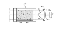
図4に第4実施形態に係る原子発振器10の概略図を示す。第4実施形態に係る原子発振器10の基本的構成は、第1実施形態乃至第3実施形態の構成に加えて、ガスセル12の光検出器16側の光軸O上に、レーザ光18の光束を収束して平行光72(86)を形成可能なレンズ群74(レンズ群80)が配設されている。図4(a)はレンズ群74を用いた場合の概略図、図4(b)はレンズ群80を用いた場合の概略図である。第4実施形態は第1実施形態乃至第3実施形態とは構造的に何ら干渉しないため、第4実施形態は第1実施形態乃至第3実施形態と同時に構成可能であり、後述の第5実施形態、第6実施形態も同様である。
FIG. 4 shows a schematic diagram of an
光検出器は受光面積が大きくなると暗電流が増大し、S/N比が低下する場合があるため、受光面積が小さいものが用いられる場合がある。ところが第1実施形態乃至第3実施形態の場合のようにレーザ光18の光束が拡張されたままであると、受光面積が小さい光検出器88ではガスセルを透過する全てのレーザ光18(出射光34、58、70)を捉えきれないため、EIT信号が小さくなる。そこでガスセル12の後段に上述のレンズ群74(レンズ群80)を配設している。
A photodetector having a small light receiving area may be used because the dark current increases and the S / N ratio may decrease as the light receiving area increases. However, if the luminous flux of the
レンズ群74(レンズ群80)は、光束が拡張されたレーザ光18の光束を収束する凸レンズ76(凸レンズ82)と、収束したレーザ光18の光束を平行光に調整する凸レンズ78(凹レンズ84)とから構成される。よってレンズ群72(レンズ群78)は、第2実施形態に係るレンズ群42(レンズ群48)の前後配置を光軸O上で逆にして、ガスセル12と光検出器88との間に配設したものと同様である。よって、レーザ光18の収束比(拡張比の逆数)は第2実施形態と同様に各レンズの焦点距離、及びレンズ間の距離によって決定される。
The lens group 74 (lens group 80) includes a convex lens 76 (convex lens 82) that converges the light beam of the
よって第4実施形態によれば、収束比を適切に調整することにより、出射光34、58、70を後段の光検出器の受光面の大きさに合わせた平行光に形成可能となる。さらに平行光であるから、光検出器88の位置を光軸O上であれば自由に設計することができる。 Therefore, according to the fourth embodiment, by appropriately adjusting the convergence ratio, the emitted lights 34, 58, and 70 can be formed into parallel lights matching the size of the light receiving surface of the subsequent photodetector. Furthermore, since it is parallel light, if the position of the photodetector 88 is on the optical axis O, it can be designed freely.
図5に第5実施形態に係る原子発振器の概略図を示す。第5実施形態に係る原子発振器の基本的構成は、第1実施形態乃至第3実施形態の構成に加えて、ガスセル12の光検出器16側の光軸O上に凸レンズ90を配設している。
FIG. 5 shows a schematic diagram of an atomic oscillator according to the fifth embodiment. The basic configuration of the atomic oscillator according to the fifth embodiment includes a convex lens 90 disposed on the optical axis O on the photodetector 16 side of the
凸レンズ90の直径は、その配設位置において出射光34、58、70のいずれの場合においても捉えきれる大きさが必要である。第1実施形態に本実施形態を適用する場合において、凸レンズ90の焦点距離を、凸レンズ90の設置位置と第1実施形態に係る凸レンズ24または凹レンズ26の焦点位置との距離よりも短くなるように設計すれば、第1実施形態に係る出射光34は凸レンズ90によって収束する。なお、上記焦点位置との距離と同じ場合、出射光34は凸レンズ90によって平行光となる。第2実施形態の出射光58、第3実施形態の出射光70は平行光であるので凸レンズ90を透過すると、凸レンズ90の焦点距離分進行した点で焦点を結び、その後は再びその光束は拡張する。
The diameter of the convex lens 90 needs to be large enough to be captured in any case of the emitted light 34, 58, and 70 at the arrangement position. When this embodiment is applied to the first embodiment, the focal length of the convex lens 90 is made shorter than the distance between the installation position of the convex lens 90 and the focal position of the
よって光検出器92の光軸O上の位置を適切に設計することにより、光検出器92の受光面の大きさに合わせた光束を選択可能となる。また第4実施形態のようにレンズを複数
枚用いる必要はないので、設計が容易となり第4実施形態よりもコストダウンを図ることができる。
Therefore, by appropriately designing the position of the photodetector 92 on the optical axis O, it becomes possible to select a light flux that matches the size of the light receiving surface of the photodetector 92. In addition, since it is not necessary to use a plurality of lenses as in the fourth embodiment, the design is facilitated and the cost can be reduced as compared with the fourth embodiment.
図6に第6実施形態に係る原子発振器の概略図を示す。第6実施形態に係る原子発振器の基本的構成は、第1実施形態乃至第3実施形態の構成に加えて、ガスセル12の光検出器16側の光軸O上には、レーザ光12の光束(出射光34、58、70)を収束して平行光94を形成可能な反射鏡群96が配設されている。
FIG. 6 shows a schematic diagram of an atomic oscillator according to the sixth embodiment. The basic configuration of the atomic oscillator according to the sixth embodiment includes the luminous flux of the
反射鏡群96は拡張した出射光34、58、70の光束を反射して収束する主鏡98と、収束した出射光34、58、70の光束を反射して平行光に調整する副鏡100とから構成されている。よって反射鏡群96は第3実施形態の反射鏡群60の光軸O上の前後配置を逆にして、ガスセル12と光検出器102との間に配設したものと同様である。よってレーザ光12の収束比は第3実施形態同様に各反射鏡の焦点距離、及び反射鏡間の距離によって決定される。また第3実施形態同様に反射鏡群96において色収差は発生しないので、収束比には波長依存性はなく、反射鏡群96を通過したレーザ光の光束の直径は波長によらず一定である。
The reflecting
したがって第6実施形態によれば、収束比を適切に調整することにより第4実施形態と同様の効果を有する。また第3実施形態と同様に、反射鏡はガスセル12を収納するケーシング(不図示)の内側に曲率を与え鏡面処理することによっても得られるので、大掛かりな光学系を必要とせず、コストダウンを図ることができる。
Therefore, according to the sixth embodiment, an effect similar to that of the fourth embodiment is obtained by appropriately adjusting the convergence ratio. Similarly to the third embodiment, the reflecting mirror can also be obtained by applying a curvature to the inside of a casing (not shown) that houses the
さらに、反射鏡群96を通過したレーザ光18の直径は波長によらず一定であり、光検出器に到達する光束の直径(幅)は波長によって変化しないので、光学系に起因するS/N比の波長依存性を低減した高品質なEIT信号を得ることができ、特に第3実施形態に第6実施形態を用いた場合は、レーザ光18の全ての光路上において上述の波長依存性がなくなるので、その効果は顕著となる。
Further, the diameter of the
ガスセルの内壁近傍の金属原子にレーザ光を照射するとEIT信号の品質が低下することについてはすでに述べた。そこでガスセルの内壁からどの程度はなれた距離の金属原子にレーザを照射すべきかについて述べる。 It has already been described that the quality of the EIT signal is lowered when laser light is irradiated to metal atoms in the vicinity of the inner wall of the gas cell. Therefore, how far the metal atoms should be irradiated from the inner wall of the gas cell should be described.
図7(a)に、ガスセルと光束が拡張されたレーザ光との関係を示した概略図を示す。ガスセル12内には金属原子30のみが気体として存在していると仮定する。このとき金属原子30はガスセル12内でガスセル12内の温度や圧力等に依存した速度で、他の金属原子30と衝突しつつ運動している。金属原子30が全て均一な速度で運動している場合は、その平均自由行程(他の金属原子に衝突するまで進行可能な距離の平均値)λは、
因となり、図8(b)に示すように、レーザ光18の光束の外周と壁面との距離Lが平均自由行程λ以下になった場合には、EIT信号の半値幅は著しく増大するものと考えられる。
FIG. 7A is a schematic diagram showing the relationship between the gas cell and the laser beam with the expanded light beam. Assume that only the
したがって、レーザ光18の光束を光束拡張手段22によって拡張する場合は、図7(a)に示すように、本発明に最適なガスセル12の内壁から内部空間20(直径D0)側の距離Lが、ガスセル12の内壁から内部区間20側に、ガスセル12に存在する金属原子の平均自由行程λ以上の長さとなるようにレーザ光18の光束の直径を調整する必要がある。すなわち、ガスセル12の内壁からλ以上離れた金属原子30にレーザを照射する必要がある。このとき、レーザ光18の光束の直径の最大値Dλは、
本発明において、直径D0は10mm程度である。また実際のガスセル12内部の金属原子30のみならず他の気体も混在しているが、その真空度は1Torr前後に保たれており、このとき気体の平均自由行程は100μm程度の大きさであるから、金属原子の平均自由行程λも同程度の長さを有するものと考えられる。よって本発明において、9.8mm程度の幅を最大値(Dλ)としてレーザ光18の拡張比を調整する必要がある。
In the present invention, the diameter D 0 is about 10 mm. Further, not only the
図8に第7実施形態に係る原子発振器を組み込んだ発振デバイスを示す概略図(正面図)ある。
図8(a)に示すように、第7実施形態に係る原子発振器を組み込んだ発振デバイス110はケーシング112、レーザ光発振源114、光束拡張手段116、ガスセル118、光束収束手段120、光検出器122とから構成されている。ケーシング112は一端を開口した壷を逆さまにしたような形状で、一定の剛性を有する筐体であり、前記開口した部分を下にして基板124に固定されている。また、その内部にレーザ光発振源114、光束拡張手段116、ガスセル118、光収束手段120、光検出器122を包含している。レーザ光発振源114は、第1実施形態で述べたレーザ光発振源14と同様の構成でレーザ光126を発するもので、その下端に固定用のダボ(棒)128が配設され、上端にはレーザ光126が出射されるレンズ130が配設されている。さらに上端にはレンズ130を上端に露出させつつ周囲を囲むように、後述のユニット136を固定するための平板状の土台132が配設されている。そして基板124のケーシング112の開口部分によって囲まれた部分に形成されたダボ穴134に前記ダボ128を挿入することにより、レーザ光発振源126は基板124に固定される。
FIG. 8 is a schematic view (front view) showing an oscillation device incorporating the atomic oscillator according to the seventh embodiment.
As shown in FIG. 8A, the oscillation device 110 incorporating the atomic oscillator according to the seventh embodiment includes a casing 112, a laser light oscillation source 114, a light beam expanding means 116, a
光束拡張手段116、ガスセル118、光束収束手段120、光検出器122は一体型のユニット136を形成しており、上述の順番に下から積みあがって接着固定されている。光束拡張手段116は上述の第1実施形態乃至第3実施形態のいずれかに記載の光束拡張手段22と同様の形態をもつ。ガスセル118は金属原子138を封入した中空の筐体であり、その上面および下面にはガスセル保護用のコーティング膜140(波長板等含む)が介装されている。
The light beam expanding means 116, the
光束収束手段120は上述の第4実施形態乃至第6実施形態に記載されたいずれかのレンズ状の形態をもつ。光検出器122は光収束手段120と固定するための固定材142に埋め込まれ、受光面144を固定材142の下端に露出させている。そして前記ユニット136はその下端とレーザ光発振源114の上端にある土台132とを、ばね等の弾性体146を介して固定されている。またユニット136の側面とケーシング112の内壁との間も弾性体148を介して固定されている。 The light beam converging means 120 has one of the lens-like forms described in the fourth to sixth embodiments. The photodetector 122 is embedded in a fixing material 142 for fixing to the light converging means 120, and the light receiving surface 144 is exposed at the lower end of the fixing material 142. The unit 136 has its lower end fixed to the base 132 at the upper end of the laser beam oscillation source 114 via an elastic body 146 such as a spring. Further, the side surface of the unit 136 and the inner wall of the casing 112 are also fixed via an elastic body 148.
ケーシング側面及び上面にはねじ穴154、156があけられ、それぞれのねじ穴154、156には調整ねじ150、152がねじ込まれている。調整ねじ150の先端はユニット136(光束拡張手段116)の側面に当接している。また調整ねじ152はユニット136(光検出器122)の上端に当接している。 Screw holes 154 and 156 are formed in the side surface and the upper surface of the casing, and adjustment screws 150 and 152 are screwed into the screw holes 154 and 156, respectively. The tip of the adjustment screw 150 is in contact with the side surface of the unit 136 (light beam expanding means 116). The adjusting screw 152 is in contact with the upper end of the unit 136 (the photodetector 122).
弾性体146はユニット136を上方に付勢可能であり、調整ねじ152によるユニット136への上からの押し付けがないとき、ユニット136の釣り合いの位置は、ユニット136の光軸上の最適なアライメント位置より上方(調整ねじ152側)に位置するものとする。また弾性体148はユニット136を側面から調整ねじ150の方向に付勢可能であり、調整ねじ152による側面からの押し付けがなく弾性体148が無付勢であるときは、ユニット136はレーザ光126の光軸より調整ねじ150側に位置するものとする。また調整ねじ150、152は一定の剛性を有するケーシング112に保持される関係にあり、調整ねじ150、152からの反力を受けても動かないので、調整ねじ150、152はユニット136へ押し付け力を与えることができる。これによりユニット136はレーザ光発振源114に固定されつつも一定の範囲で自由に動かすことができ、光軸調整をしてユニット136を最適なアライメント位置に固定することが可能となる。光軸調整はレーザ光126を発振させ、光検出器122でレーザ光126を検出しながら、光検出器122が検出するレーザ光126の強度が最大となるように調整ねじ150、152を回すことによりユニット136の位置を調整することが可能となる。 The elastic body 146 can urge the unit 136 upward, and when the adjustment screw 152 does not press the unit 136 from above, the balance position of the unit 136 is the optimum alignment position on the optical axis of the unit 136. It is assumed to be located above (adjustment screw 152 side). The elastic body 148 can urge the unit 136 from the side surface in the direction of the adjusting screw 150. When the elastic body 148 is not urged without being pressed from the side surface by the adjusting screw 152, the unit 136 emits the laser beam 126. It is assumed that it is located on the adjustment screw 150 side from the optical axis. Further, the adjusting screws 150 and 152 are held by the casing 112 having a certain rigidity, and do not move even when receiving the reaction force from the adjusting screws 150 and 152, so that the adjusting screws 150 and 152 are pressed against the unit 136. Can be given. As a result, the unit 136 can be freely moved within a certain range while being fixed to the laser beam oscillation source 114, and the unit 136 can be fixed at the optimum alignment position by adjusting the optical axis. To adjust the optical axis, the laser light 126 is oscillated and the adjusting screws 150 and 152 are rotated so that the intensity of the laser light 126 detected by the photodetector 122 is maximized while detecting the laser light 126 by the photodetector 122. Thus, the position of the unit 136 can be adjusted.
また図8(b)に示すように、調整ねじ150、152の代わりに電流調整により長さを変えられる圧電素子等で形成されたアクチュエータ158(横方向に伸縮可能)、160(縦方向に伸縮可能)をケーシング内壁とユニットとの間に介装して接合することによっても行うことができる。これによりケーシング112にねじ穴を開ける必要はなく、弾性体146、148も不要であり、手作業なしに電流調整のみで光軸調整を行うことができる。 Further, as shown in FIG. 8B, actuators 158 (extendable / contractible in the horizontal direction) and 160 (extensible / contractible in the vertical direction) formed of piezoelectric elements or the like whose length can be changed by adjusting the current instead of the adjusting screws 150, 152 Can be performed by interposing between the inner wall of the casing and the unit. Accordingly, there is no need to make a screw hole in the casing 112, the elastic bodies 146 and 148 are unnecessary, and the optical axis can be adjusted only by current adjustment without manual work.
さらに図8(c)に示すように、土台132とユニット136とをアクチュエータ162、164を介して接合することもできる。アクチュエータ162、164はアクチュエータ158等と同様に圧電素子等で形成されている。またアクチュエータ162、164は同一の特性のものを用いればよい。両者に同一の電流が流れているときは同じ長さになっているとする。また両者は独立に電流調整が可能であるものとする。よって両者に同一の大きさの電流を流しつつ、その値を変化させるとユニット136は矢印166に示すように上下にシフトし、両者に異なった値の電流を流すとユニット136は矢印168に示すように傾斜させることができる。
したがって第7実施形態においては、第1実施形態乃至第6実施形態のいずれかの原子発振器を組み込むことにより高品質かつ大きなEIT信号を得られる発振デバイスとなる。
Further, as shown in FIG. 8C, the base 132 and the unit 136 can be joined via the actuators 162 and 164. The actuators 162 and 164 are formed of piezoelectric elements or the like, like the actuator 158 and the like. The actuators 162 and 164 may have the same characteristics. When the same current flows through both, it is assumed that the length is the same. In addition, both of them can be adjusted independently. Therefore, when the current of the same magnitude is supplied to both of them and the value is changed, the unit 136 is shifted up and down as shown by an arrow 166, and when currents of different values are supplied to the two, the unit 136 is shown by an arrow 168. Can be tilted.
Therefore, in the seventh embodiment, an oscillation device capable of obtaining a high quality and large EIT signal by incorporating the atomic oscillator of any of the first to sixth embodiments.
なお、いずれの実施形態においてもガスセル12の内部空間20の形状は円筒形であることを前提として述べてきたが、光束が拡張されたレーザ光18がガスセルの胴体40に当たらない構成であれば他の形状、たとえば断面が矩形の角柱形、断面が6角型の6角柱形でも良い。
In any of the embodiments, the shape of the
10………原子発振器、12………ガスセル、14………レーザ光発振源、16………光検出器、18………レーザ光、20………内部空間、22………光束拡張手段、24………凸レンズ、26………凹レンズ、28………終端部、30………金属原子、32………周波数制御回路、34………出射光、36………入射窓、38………出射窓、40………胴体、42………レンズ群、44………凸レンズ、46………凸レンズ、48………レンズ群、50………凹レンズ、52………凸レンズ、54………平行光、56………平行光、58………出射光、60………反射鏡群、62………副鏡、64………主鏡、66………入射窓、68………平行光、70………出射光、72………平行光、74………レンズ群、76………凸レンズ、78………凸レンズ、80………レンズ群、82………凸レンズ、84………凹レンズ、86………平行光、88………光検出器、90………凸レンズ、92………光検出器、94………平行光、96………反射鏡群、98………主鏡、100………副鏡、102………光検出器、110………発振デバイス、112………ケーシング、114………レーザ光発振源、116………光束拡張手段、118………ガスセル、120………光束収束手段、122………光検出器、124………基板、126………レーザ光、128………ダボ、130………レンズ、132………土台、134………ダボ穴、136………ユニット、138………金属原子、140………コーティング薄膜、142………固定材、144………受光面、146………弾性体、148………弾性体、150………調整ねじ、152………調整ねじ、154………ねじ穴、156………ねじ穴、158………アクチュエータ、160………アクチュエータ、162………アクチュエータ、164………アクチュエータ、166………矢印、168………矢印、200………原子発振器、202………半導体レーザ、204………ガスセル、206………光検出器、208………周波数制御回路。
DESCRIPTION OF
Claims (10)
ガス状の金属原子を封入したガスセルと、前記ガスセル中の金属原子に前記共鳴光を供給するコヒーレント光源と、前記ガスセルを透過した光を検出する光検出器と、を備え
コヒーレント光源と前記ガスセルとの間の光軸上には、コヒーレント光の光束を前記ガスセルの内部空間より狭い範囲で拡張可能な光束拡張手段が配設されたことを特徴とする原子発振器。 An optical system of an atomic oscillator that controls an oscillation frequency by utilizing a light absorption characteristic by a quantum interference effect when two types of resonant light are incident as coherent light having different wavelengths,
A gas cell in which gaseous metal atoms are enclosed; a coherent light source that supplies the resonance light to the metal atoms in the gas cell; and a photodetector that detects light transmitted through the gas cell; a coherent light source and the gas cell; An atomic oscillator characterized in that a light beam expanding means capable of expanding a light beam of coherent light in a range narrower than the internal space of the gas cell is disposed on the optical axis between the two.
Priority Applications (1)
| Application Number | Priority Date | Filing Date | Title |
|---|---|---|---|
| JP2008000364A JP2009164331A (en) | 2008-01-07 | 2008-01-07 | Atomic oscillator and oscillation device |
Applications Claiming Priority (1)
| Application Number | Priority Date | Filing Date | Title |
|---|---|---|---|
| JP2008000364A JP2009164331A (en) | 2008-01-07 | 2008-01-07 | Atomic oscillator and oscillation device |
Publications (1)
| Publication Number | Publication Date |
|---|---|
| JP2009164331A true JP2009164331A (en) | 2009-07-23 |
Family
ID=40966612
Family Applications (1)
| Application Number | Title | Priority Date | Filing Date |
|---|---|---|---|
| JP2008000364A Withdrawn JP2009164331A (en) | 2008-01-07 | 2008-01-07 | Atomic oscillator and oscillation device |
Country Status (1)
| Country | Link |
|---|---|
| JP (1) | JP2009164331A (en) |
Cited By (14)
| Publication number | Priority date | Publication date | Assignee | Title |
|---|---|---|---|---|
| JP2012049230A (en) * | 2010-08-25 | 2012-03-08 | Seiko Epson Corp | Quantum interference device and method of quantum interference |
| JP2013171881A (en) * | 2012-02-17 | 2013-09-02 | Seiko Epson Corp | Atomic oscillator |
| US8803618B2 (en) | 2011-03-14 | 2014-08-12 | Seiko Epson Corporation | Optical module for atomic oscillator and atomic oscillator |
| US8830005B2 (en) | 2011-03-23 | 2014-09-09 | Seiko Epson Corporation | Optical module for atomic oscillator and atomic oscillator |
| US8836437B2 (en) | 2011-03-14 | 2014-09-16 | Seiko Epson Corporation | Optical module for atomic oscillator and atomic oscillator |
| US8878617B2 (en) | 2012-01-11 | 2014-11-04 | Seiko Epson Corporation | Optical module for atomic oscillator and atomic oscillator |
| JP2015057841A (en) * | 2014-10-31 | 2015-03-26 | セイコーエプソン株式会社 | Quantum interference device |
| JP2015070228A (en) * | 2013-09-30 | 2015-04-13 | セイコーエプソン株式会社 | Quantum interference device, atomic oscillator, electronic apparatus and mobile |
| US9054638B2 (en) | 2010-07-14 | 2015-06-09 | Seiko Epson Corporation | Optical module and atomic oscillator |
| US9200964B2 (en) | 2013-11-01 | 2015-12-01 | Seiko Epson Corporation | Optical module and atomic oscillator |
| US9444477B2 (en) | 2013-12-20 | 2016-09-13 | Seiko Epson Corporation | Quantum interference device, atomic oscillator, electronic apparatus, and moving object |
| US9503111B2 (en) | 2014-09-29 | 2016-11-22 | Seiko Epson Corporation | Atomic oscillator |
| JP2017183313A (en) * | 2016-03-28 | 2017-10-05 | セイコーエプソン株式会社 | Quantum interference devices, atomic oscillators, electronic equipment, and moving objects |
| WO2018074031A1 (en) * | 2016-10-19 | 2018-04-26 | 株式会社村田製作所 | Atomic oscillator and electronic device |
Citations (10)
| Publication number | Priority date | Publication date | Assignee | Title |
|---|---|---|---|---|
| JPS5577186A (en) * | 1978-12-05 | 1980-06-10 | Seiko Epson Corp | Atomic frequency standard |
| JPS62145925A (en) * | 1985-12-20 | 1987-06-30 | Fujitsu Ltd | Gas cell type atomic oscillator |
| JPS62162861U (en) * | 1986-04-03 | 1987-10-16 | ||
| JPS649674A (en) * | 1987-07-01 | 1989-01-12 | Fujitsu Ltd | Exciting light-emitting lamp for gas cell type atomic oscillator |
| JPH01274482A (en) * | 1988-04-27 | 1989-11-02 | Nec Corp | Rubidium atomic oscillator |
| JPH02117185A (en) * | 1988-10-27 | 1990-05-01 | Nec Corp | Rubidium atomic oscillator |
| JPH03139889A (en) * | 1989-10-25 | 1991-06-14 | Nec Corp | Rubidium atom oscillator |
| JPH07142784A (en) * | 1993-11-17 | 1995-06-02 | Nec Corp | Rubidium atom oscillator |
| JPH10284772A (en) * | 1997-03-31 | 1998-10-23 | Anritsu Corp | Atomic oscillator |
| JP2007336136A (en) * | 2006-06-14 | 2007-12-27 | Epson Toyocom Corp | Atomic oscillator, passive atomic oscillator, temperature control method for atomic oscillator, and temperature control method for passive atomic oscillator |
-
2008
- 2008-01-07 JP JP2008000364A patent/JP2009164331A/en not_active Withdrawn
Patent Citations (10)
| Publication number | Priority date | Publication date | Assignee | Title |
|---|---|---|---|---|
| JPS5577186A (en) * | 1978-12-05 | 1980-06-10 | Seiko Epson Corp | Atomic frequency standard |
| JPS62145925A (en) * | 1985-12-20 | 1987-06-30 | Fujitsu Ltd | Gas cell type atomic oscillator |
| JPS62162861U (en) * | 1986-04-03 | 1987-10-16 | ||
| JPS649674A (en) * | 1987-07-01 | 1989-01-12 | Fujitsu Ltd | Exciting light-emitting lamp for gas cell type atomic oscillator |
| JPH01274482A (en) * | 1988-04-27 | 1989-11-02 | Nec Corp | Rubidium atomic oscillator |
| JPH02117185A (en) * | 1988-10-27 | 1990-05-01 | Nec Corp | Rubidium atomic oscillator |
| JPH03139889A (en) * | 1989-10-25 | 1991-06-14 | Nec Corp | Rubidium atom oscillator |
| JPH07142784A (en) * | 1993-11-17 | 1995-06-02 | Nec Corp | Rubidium atom oscillator |
| JPH10284772A (en) * | 1997-03-31 | 1998-10-23 | Anritsu Corp | Atomic oscillator |
| JP2007336136A (en) * | 2006-06-14 | 2007-12-27 | Epson Toyocom Corp | Atomic oscillator, passive atomic oscillator, temperature control method for atomic oscillator, and temperature control method for passive atomic oscillator |
Cited By (24)
| Publication number | Priority date | Publication date | Assignee | Title |
|---|---|---|---|---|
| US9054638B2 (en) | 2010-07-14 | 2015-06-09 | Seiko Epson Corporation | Optical module and atomic oscillator |
| JP2012049230A (en) * | 2010-08-25 | 2012-03-08 | Seiko Epson Corp | Quantum interference device and method of quantum interference |
| US8803618B2 (en) | 2011-03-14 | 2014-08-12 | Seiko Epson Corporation | Optical module for atomic oscillator and atomic oscillator |
| US8836437B2 (en) | 2011-03-14 | 2014-09-16 | Seiko Epson Corporation | Optical module for atomic oscillator and atomic oscillator |
| US8830005B2 (en) | 2011-03-23 | 2014-09-09 | Seiko Epson Corporation | Optical module for atomic oscillator and atomic oscillator |
| US8878617B2 (en) | 2012-01-11 | 2014-11-04 | Seiko Epson Corporation | Optical module for atomic oscillator and atomic oscillator |
| US9294109B2 (en) | 2012-01-11 | 2016-03-22 | Seiko Epson Corporation | Optical module for atomic oscillator and atomic oscillator |
| JP2013171881A (en) * | 2012-02-17 | 2013-09-02 | Seiko Epson Corp | Atomic oscillator |
| JP2015070228A (en) * | 2013-09-30 | 2015-04-13 | セイコーエプソン株式会社 | Quantum interference device, atomic oscillator, electronic apparatus and mobile |
| CN104518794A (en) * | 2013-09-30 | 2015-04-15 | 精工爱普生株式会社 | Quantum interference device, atomic oscillator, electronic apparatus, and moving object |
| US9200964B2 (en) | 2013-11-01 | 2015-12-01 | Seiko Epson Corporation | Optical module and atomic oscillator |
| US9768791B2 (en) | 2013-12-20 | 2017-09-19 | Seiko Epson Corporation | Quantum interference device, atomic oscillator, electronic apparatus, and moving object |
| US9444477B2 (en) | 2013-12-20 | 2016-09-13 | Seiko Epson Corporation | Quantum interference device, atomic oscillator, electronic apparatus, and moving object |
| US9503111B2 (en) | 2014-09-29 | 2016-11-22 | Seiko Epson Corporation | Atomic oscillator |
| JP2015057841A (en) * | 2014-10-31 | 2015-03-26 | セイコーエプソン株式会社 | Quantum interference device |
| JP2017183313A (en) * | 2016-03-28 | 2017-10-05 | セイコーエプソン株式会社 | Quantum interference devices, atomic oscillators, electronic equipment, and moving objects |
| CN107241095A (en) * | 2016-03-28 | 2017-10-10 | 精工爱普生株式会社 | Quantum interference device, atomic oscillator, electronic equipment and moving body |
| US10326461B2 (en) | 2016-03-28 | 2019-06-18 | Seiko Epson Corporation | Quantum interference device, atomic oscillator, electronic apparatus, and moving object |
| CN107241095B (en) * | 2016-03-28 | 2022-08-26 | 精工爱普生株式会社 | Quantum interference device, atomic oscillator, and electronic apparatus |
| WO2018074031A1 (en) * | 2016-10-19 | 2018-04-26 | 株式会社村田製作所 | Atomic oscillator and electronic device |
| JPWO2018074031A1 (en) * | 2016-10-19 | 2019-03-28 | 株式会社村田製作所 | Atomic oscillator and electronic equipment |
| CN109565283A (en) * | 2016-10-19 | 2019-04-02 | 株式会社村田制作所 | Atomic oscillator and electronic equipment |
| US10756743B2 (en) | 2016-10-19 | 2020-08-25 | Murata Manufacturing Co., Ltd. | Atomic oscillator and electronic device |
| CN109565283B (en) * | 2016-10-19 | 2023-07-07 | 株式会社村田制作所 | Atomic oscillator and electronic apparatus |
Similar Documents
| Publication | Publication Date | Title |
|---|---|---|
| JP2009164331A (en) | Atomic oscillator and oscillation device | |
| JP5343356B2 (en) | Atomic oscillator | |
| JP5368261B2 (en) | Extreme ultraviolet light source device, control method of extreme ultraviolet light source device | |
| RU2539970C2 (en) | Laser-pumped light source and method for generation of light emission | |
| JP2010087388A (en) | Aligner | |
| CN102185250A (en) | Device and method for generating femtosecond time-resolved X-ray source | |
| Heissler et al. | Multi-μJ harmonic emission energy from laser-driven plasma | |
| KR101269115B1 (en) | Structure is simplified euv plasma generating apparatus | |
| US9888555B2 (en) | Transmission system for transmitting pulse laser beam to extreme ultraviolet light chamber, and laser system | |
| JP2006032322A (en) | Apparatus for temporally stable generation of EUV radiation using a laser-induced plasma | |
| US9036251B2 (en) | Slab amplification device, laser apparatus, and extreme ultraviolet light generation system | |
| JP2014041828A (en) | Extreme ultraviolet light source device | |
| US9762024B2 (en) | Laser apparatus and extreme ultraviolet light generation system | |
| RU2013146435A (en) | DISK LASER | |
| WO2019116461A1 (en) | Far-infrared light source and far-infrared spectrometer | |
| US20150097107A1 (en) | Apparatus for generating extreme ultraviolet light using plasma | |
| KR101401241B1 (en) | EUV beam generating device to implement the alignment | |
| US20190239329A1 (en) | Extreme ultraviolet light generation apparatus | |
| CN110492347B (en) | Deep ultraviolet angle-resolved photoelectron spectroscopy light source with spatial resolution capability | |
| US20130092849A1 (en) | Laser device, laser apparatus, and extreme ultraviolet light generation system | |
| JP6390863B2 (en) | Laser drive light source device | |
| WO2023243352A1 (en) | Spectroscopic analysis device | |
| KR101359754B1 (en) | Precision adjustable optical EUV light generating device | |
| TW202314362A (en) | Euv light source with a separation device | |
| KR101324545B1 (en) | Laser beam through the stabilization and calibration for EUV generation device to improve energy efficiency |
Legal Events
| Date | Code | Title | Description |
|---|---|---|---|
| A621 | Written request for application examination |
Effective date: 20110105 Free format text: JAPANESE INTERMEDIATE CODE: A621 |
|
| A711 | Notification of change in applicant |
Free format text: JAPANESE INTERMEDIATE CODE: A712 Effective date: 20110729 |
|
| RD03 | Notification of appointment of power of attorney |
Effective date: 20110729 Free format text: JAPANESE INTERMEDIATE CODE: A7423 |
|
| A521 | Written amendment |
Effective date: 20110819 Free format text: JAPANESE INTERMEDIATE CODE: A523 |
|
| A131 | Notification of reasons for refusal |
Free format text: JAPANESE INTERMEDIATE CODE: A131 Effective date: 20130416 |
|
| A761 | Written withdrawal of application |
Free format text: JAPANESE INTERMEDIATE CODE: A761 Effective date: 20130516 |