JP2009183111A - Charge pump circuit and electronic device including the same - Google Patents
Charge pump circuit and electronic device including the same Download PDFInfo
- Publication number
- JP2009183111A JP2009183111A JP2008021475A JP2008021475A JP2009183111A JP 2009183111 A JP2009183111 A JP 2009183111A JP 2008021475 A JP2008021475 A JP 2008021475A JP 2008021475 A JP2008021475 A JP 2008021475A JP 2009183111 A JP2009183111 A JP 2009183111A
- Authority
- JP
- Japan
- Prior art keywords
- voltage
- circuit
- charge pump
- node
- protection
- Prior art date
- Legal status (The legal status is an assumption and is not a legal conclusion. Google has not performed a legal analysis and makes no representation as to the accuracy of the status listed.)
- Pending
Links
Images






Classifications
-
- H—ELECTRICITY
- H02—GENERATION; CONVERSION OR DISTRIBUTION OF ELECTRIC POWER
- H02M—APPARATUS FOR CONVERSION BETWEEN AC AND AC, BETWEEN AC AND DC, OR BETWEEN DC AND DC, AND FOR USE WITH MAINS OR SIMILAR POWER SUPPLY SYSTEMS; CONVERSION OF DC OR AC INPUT POWER INTO SURGE OUTPUT POWER; CONTROL OR REGULATION THEREOF
- H02M3/00—Conversion of DC power input into DC power output
- H02M3/02—Conversion of DC power input into DC power output without intermediate conversion into AC
- H02M3/04—Conversion of DC power input into DC power output without intermediate conversion into AC by static converters
- H02M3/06—Conversion of DC power input into DC power output without intermediate conversion into AC by static converters using resistors or capacitors, e.g. potential divider
- H02M3/07—Conversion of DC power input into DC power output without intermediate conversion into AC by static converters using resistors or capacitors, e.g. potential divider using capacitors charged and discharged alternately by semiconductor devices with control electrode, e.g. charge pumps
-
- H—ELECTRICITY
- H02—GENERATION; CONVERSION OR DISTRIBUTION OF ELECTRIC POWER
- H02M—APPARATUS FOR CONVERSION BETWEEN AC AND AC, BETWEEN AC AND DC, OR BETWEEN DC AND DC, AND FOR USE WITH MAINS OR SIMILAR POWER SUPPLY SYSTEMS; CONVERSION OF DC OR AC INPUT POWER INTO SURGE OUTPUT POWER; CONTROL OR REGULATION THEREOF
- H02M1/00—Details of apparatus for conversion
- H02M1/32—Means for protecting converters other than automatic disconnection
-
- H—ELECTRICITY
- H02—GENERATION; CONVERSION OR DISTRIBUTION OF ELECTRIC POWER
- H02M—APPARATUS FOR CONVERSION BETWEEN AC AND AC, BETWEEN AC AND DC, OR BETWEEN DC AND DC, AND FOR USE WITH MAINS OR SIMILAR POWER SUPPLY SYSTEMS; CONVERSION OF DC OR AC INPUT POWER INTO SURGE OUTPUT POWER; CONTROL OR REGULATION THEREOF
- H02M3/00—Conversion of DC power input into DC power output
- H02M3/02—Conversion of DC power input into DC power output without intermediate conversion into AC
- H02M3/04—Conversion of DC power input into DC power output without intermediate conversion into AC by static converters
- H02M3/06—Conversion of DC power input into DC power output without intermediate conversion into AC by static converters using resistors or capacitors, e.g. potential divider
- H02M3/07—Conversion of DC power input into DC power output without intermediate conversion into AC by static converters using resistors or capacitors, e.g. potential divider using capacitors charged and discharged alternately by semiconductor devices with control electrode, e.g. charge pumps
- H02M3/072—Conversion of DC power input into DC power output without intermediate conversion into AC by static converters using resistors or capacitors, e.g. potential divider using capacitors charged and discharged alternately by semiconductor devices with control electrode, e.g. charge pumps adapted to generate an output voltage whose value is lower than the input voltage
Landscapes
- Engineering & Computer Science (AREA)
- Power Engineering (AREA)
- Dc-Dc Converters (AREA)
Abstract
【課題】昇圧効率(または降圧効率)を低下させることなくチャージポンプ回路の過電流を抑制する。
【解決手段】出力電圧Voutが所定の判定電圧よりも高い場合、保護トランジスタT101,T104はオフ状態であり、駆動トランジスタT1,T4は、それぞれ、制御信号Sc1,Sc4に応答してオン/オフする。出力電圧Voutが判定電圧よりも低くなると、保護トランジスタT101,T104がオン状態になり、駆動トランジスタT1,T4のゲートが設定ノードNsetに接続され、駆動トランジスタT1,T4が強制的にオフ状態になる。
【選択図】図1An overcurrent of a charge pump circuit is suppressed without reducing boosting efficiency (or step-down efficiency).
When an output voltage Vout is higher than a predetermined determination voltage, protection transistors T101 and T104 are in an off state, and drive transistors T1 and T4 are turned on / off in response to control signals Sc1 and Sc4, respectively. . When the output voltage Vout becomes lower than the determination voltage, the protection transistors T101 and T104 are turned on, the gates of the drive transistors T1 and T4 are connected to the setting node Nset, and the drive transistors T1 and T4 are forcibly turned off. .
[Selection] Figure 1
Description
この発明は、入力電圧を昇圧または降圧して出力電圧を出力するチャージポンプ回路に関し、さらに詳しくは、過電流による回路破壊を防止する技術に関する。 The present invention relates to a charge pump circuit that outputs or outputs an output voltage by stepping up or down an input voltage, and more particularly to a technique for preventing circuit breakdown due to overcurrent.
従来より、比較的簡単な構成で実現できる電源回路として、チャージポンプ回路が広く知られている。チャージポンプ回路には、入力電圧を昇圧することにより正の出力電圧を出力する昇圧型チャージポンプ回路と、入力電圧を降圧することにより負の出力電圧を出力する降圧型チャージポンプ回路とがある。 Conventionally, a charge pump circuit is widely known as a power supply circuit that can be realized with a relatively simple configuration. The charge pump circuit includes a step-up charge pump circuit that outputs a positive output voltage by stepping up an input voltage and a step-down charge pump circuit that outputs a negative output voltage by stepping down the input voltage.
図10は、一般的な昇圧型チャージポンプ回路の構成を示す。このチャージポンプ回路は、ポンピング容量C81に電荷を蓄積する電荷蓄積動作と、ポンピング容量C81に蓄積された電荷を転送する電荷転送動作とを交互に実行することによって、電源電圧Vddの2倍の電圧値を有する正の出力電圧Vout(=2Vdd)を出力する。 FIG. 10 shows a configuration of a general boost type charge pump circuit. The charge pump circuit alternately performs a charge accumulation operation for accumulating charges in the pumping capacitor C81 and a charge transfer operation for transferring the charges accumulated in the pumping capacitor C81, whereby a voltage twice the power supply voltage Vdd is obtained. A positive output voltage Vout (= 2Vdd) having a value is output.
電荷蓄積期間(電荷蓄積動作の実行期間)では、駆動回路801,802,803,804は、それぞれ、接地電圧Vss,電源電圧Vdd,電源電圧Vdd,出力電圧Voutを出力する。これにより、駆動トランジスタT81,T82がオン状態になるとともに駆動トランジスタT83,T84がオフ状態になるので、ポンピング容量C81は、電源電圧Vddと接地電圧Vssとの電圧差に対応する電荷(正電荷)を蓄積する。
In the charge storage period (charge storage operation execution period), the
一方、電荷転送期間(電荷転送動作の実行期間)では、駆動回路801,802,803,804は、それぞれ、出力電圧Vout,接地電圧Vss,接地電圧Vss,電源電圧Vddを出力する。これにより、駆動トランジスタT83,T84がオン状態になるとともに駆動トランジスタT81,T82がオフ状態になるので、ポンピング容量C81に蓄積された電荷(正電荷)が出力ノードNoutに転送される。
On the other hand, in the charge transfer period (charge transfer operation execution period), the
昇圧型チャージポンプ回路では、駆動トランジスタT81,T84のゲートに出力電圧Vout(2Vdd)を供給することにより、駆動トランジスタT81,T84をオフ状態にすることができる。しかし、出力ノードNoutの地絡(出力ノードNoutと意図しない低電圧ノード(例えば、接地ノード)との短絡)が発生して、出力ノードNoutにおける出力電圧Voutが電源電圧Vddよりも低くなった場合、出力電圧Voutが駆動トランジスタT81,T84のゲートに供給されても、駆動トランジスタT81,T84は、オフ状態にならずにオン状態になる。そのため、駆動トランジスタT81,T84の両方がオン状態になり、入力ノードNinと出力ノードNoutとの間に過電流が発生してしまう。 In the step-up charge pump circuit, the drive transistors T81 and T84 can be turned off by supplying the output voltage Vout (2Vdd) to the gates of the drive transistors T81 and T84. However, when a ground fault of the output node Nout (a short circuit between the output node Nout and an unintended low voltage node (for example, a ground node)) occurs, the output voltage Vout at the output node Nout becomes lower than the power supply voltage Vdd. Even when the output voltage Vout is supplied to the gates of the drive transistors T81 and T84, the drive transistors T81 and T84 are turned on without being turned off. Therefore, both the drive transistors T81 and T84 are turned on, and an overcurrent is generated between the input node Nin and the output node Nout.
〔降圧型チャージポンプ回路〕
図11は、一般的な降圧型チャージポンプ回路の構成を示す。このチャージポンプ回路は、電荷蓄積動作と電荷転送動作とを交互に実行することによって、接地電圧Vssを電源電圧Vddの分だけ降圧した負の出力電圧Vout(=−Vdd)を出力する。
[Step-down charge pump circuit]
FIG. 11 shows a configuration of a general step-down charge pump circuit. This charge pump circuit outputs a negative output voltage Vout (= −Vdd) obtained by stepping down the ground voltage Vss by the power supply voltage Vdd by alternately executing a charge accumulation operation and a charge transfer operation.
電荷蓄積期間では、駆動回路901,902,903,904は、それぞれ、電源電圧Vdd,接地電圧Vss,接地電圧Vss,出力電圧Voutを出力する。これにより、駆動トランジスタT91,T92がオン状態になるとともに駆動トランジスタT93,T94がオフ状態になるので、ポンピング容量C91は、電源電圧Vddと接地電圧Vssとの電圧差に対応する電荷(負電荷)を蓄積する。
In the charge accumulation period, the
一方、電荷転送期間では、駆動回路901,902,903,904は、それぞれ、出力電圧Vout,電源電圧Vdd,電源電圧Vdd,接地電圧Vssを出力する。これにより、駆動トランジスタT93,T94がオン状態になるとともに駆動トランジスタT91,T92がオフ状態になるので、ポンピング容量C91に蓄積された電荷(負電荷)が出力ノードNoutに転送される。
On the other hand, in the charge transfer period, the
降圧型チャージポンプ回路では、駆動トランジスタT91,T94のゲートに出力電圧Vout(−Vdd)を供給することにより、駆動トランジスタT91,T94をオフ状態にすることができる。しかし、出力ノードNoutの天絡(出力ノードNoutと意図しない高電圧ノード(例えば、電源ノード)との短絡)が発生して、出力ノードNoutにおける出力電圧Voutが接地電圧Vssよりも高くなった場合、出力電圧Voutが駆動トランジスタT91,T94のゲートに供給されても、駆動トランジスタT91,T94は、オフ状態にならずにオン状態になる。そのため、駆動トランジスタT91,T94の両方がオン状態になり、入力ノードNinと出力ノードNoutとの間に過電流が発生してしまう。 In the step-down charge pump circuit, the drive transistors T91 and T94 can be turned off by supplying the output voltage Vout (−Vdd) to the gates of the drive transistors T91 and T94. However, when a power supply fault of the output node Nout (short circuit between the output node Nout and an unintended high voltage node (for example, a power supply node)) occurs, the output voltage Vout at the output node Nout becomes higher than the ground voltage Vss. Even when the output voltage Vout is supplied to the gates of the drive transistors T91 and T94, the drive transistors T91 and T94 are turned on without being turned off. Therefore, both the drive transistors T91 and T94 are turned on, and an overcurrent is generated between the input node Nin and the output node Nout.
このように、出力ノードNoutにおける意図しない電圧変動に起因して過電流が発生するので、チャージポンプ回路が破壊されてしまうおそれがあった。 As described above, an overcurrent is generated due to an unintended voltage fluctuation at the output node Nout, so that the charge pump circuit may be destroyed.
そこで、特開2004−320862号公報(特許文献1)には、昇圧型チャージポンプ回路の入力ノードに出力電流量を調整可能な定電圧回路を接続し、チャージポンプ回路入力ノードに供給される電流量を制限することで地絡時に発生する過電流を抑制するDC−DCコンバータが開示されている。詳しくは、定電圧回路には、入力電圧を受ける入力端子とチャージポンプ回路の入力ノードに接続される出力ノードとの間に電圧制御トランジスタが設けられており、その電圧制御トランジスタのゲート電圧を制御することにより、定電圧回路の出力電流量が調整される。
しかしながら、特許文献1では、定電圧回路の電圧制御トランジスタにおいて電圧降下が発生するので、入力電圧よりも低い電圧がチャージポンプ回路に供給される。そのため、チャージポンプ回路の昇圧効率が低下してしまう。
However, in
また、特許文献1では、定電圧回路は、チャージポンプ回路よりも高い電流駆動能力を備えている必要があった。例えば、チャージポンプ回路の出力電流を500mAにするためには、定電圧回路は、1A以上の出力電流を出力する必要があった。このように、高い電流駆動能力を備えなければならないので、定電圧回路の回路規模を低減することが困難であった。
In
そこで、この発明は、チャージポンプ回路の昇圧効率(または降圧効率)を低下させるなく、過電流を抑制することを目的とする。 Therefore, an object of the present invention is to suppress overcurrent without reducing the boosting efficiency (or step-down efficiency) of the charge pump circuit.
この発明の1つの局面に従うと、チャージポンプ回路は、入力電圧を昇圧または降圧して出力電圧を出力する回路であって、ポンピング容量と、上記入力電圧を受ける入力ノードと上記ポンピング容量の一方端との間に接続される第1の駆動トランジスタと、上記出力電圧を出力するための出力ノードと上記ポンピング容量の一方端との間に接続される第2の駆動トランジスタとを含み、電荷蓄積モードにおいて上記第1の駆動トランジスタをオン状態にして上記ポンピング容量に電荷を蓄積する一方、電荷転送モードにおいて上記第2の駆動トランジスタをオン状態にして上記ポンピング容量に蓄積された電荷を上記出力ノードへ転送するポンピング回路と、所定の判定電圧と上記出力電圧との高低関係に基づいて、上記第1および第2の駆動トランジスタの少なくとも1つを上記オン状態時よりも抵抗値が高い高抵抗状態に設定する保護回路とを備える。 According to one aspect of the present invention, a charge pump circuit is a circuit that outputs or outputs an output voltage by stepping up or down an input voltage, and includes a pumping capacitor, an input node that receives the input voltage, and one end of the pumping capacitor. And a second drive transistor connected between an output node for outputting the output voltage and one end of the pumping capacitor, and a charge accumulation mode. In the charge transfer mode, the first driving transistor is turned on to store charges in the pumping capacitor, while in the charge transfer mode, the second driving transistor is turned on to store charges stored in the pumping capacitor to the output node. Based on the level relationship between the pumping circuit to transfer and a predetermined determination voltage and the output voltage, the first and second At least one of dynamic transistor and a protection circuit for setting the high resistance state resistance value higher than during the on state.
上記チャージポンプ回路では、出力ノードにおいて意図しない電圧変動が発生すると、保護回路は、第1および第2の駆動トランジスタの少なくとも1つを高抵抗状態にする。これにより、入力ノードと出力ノードとの間における過電流を抑制することができる。また、ポンピング回路の前段に電流量を調整するための構成を設けなくても良いので、チャージポンプ回路の昇圧効率を低下させることなく昇圧動作(または降圧動作)を実行することができる。さらに、保護回路の電流駆動能力は、ポンピング回路よりも小さくても良いので、従来のように回路規模を大きくしなくても良い。そのため、チャージポンプ回路の回路規模を低減することができる。 In the charge pump circuit, when an unintended voltage change occurs at the output node, the protection circuit sets at least one of the first and second drive transistors to a high resistance state. Thereby, an overcurrent between the input node and the output node can be suppressed. Further, since it is not necessary to provide a configuration for adjusting the amount of current in the previous stage of the pumping circuit, the boosting operation (or the step-down operation) can be executed without reducing the boosting efficiency of the charge pump circuit. Furthermore, since the current drive capability of the protection circuit may be smaller than that of the pumping circuit, it is not necessary to increase the circuit scale as in the prior art. Therefore, the circuit scale of the charge pump circuit can be reduced.
好ましくは、上記保護回路は、上記第1の駆動トランジスタを高抵抗状態に設定するための第1の設定電圧を受ける第1の設定ノードに接続されるソースと、上記出力ノードに接続されるゲートと、上記第1の駆動トランジスタのゲートに接続されるドレインとを有する第1の保護トランジスタを含む。 Preferably, the protection circuit includes a source connected to a first setting node that receives a first setting voltage for setting the first driving transistor in a high resistance state, and a gate connected to the output node. And a first protection transistor having a drain connected to the gate of the first driving transistor.
上記チャージポンプ回路では、第1の設定電圧と第1の駆動トランジスタの閾値電圧とで定められる判定電圧と出力ノードにおける出力電圧との高低関係に応じて、第1の駆動トランジスタのゲートと第1の設定ノードとの接続状態が切り換えられる。 In the charge pump circuit, the gate of the first drive transistor and the first voltage are determined according to the level relationship between the determination voltage determined by the first set voltage and the threshold voltage of the first drive transistor and the output voltage at the output node. The connection state with the setting node is switched.
好ましくは、上記保護回路は、上記第2の駆動トランジスタを高抵抗状態に設定するための第2の設定電圧を受ける第2の設定ノードに接続されるソースと、上記出力ノードに接続されるゲートと、上記第2の駆動トランジスタのゲートに接続されるドレインとを有する第2の保護トランジスタを含む。 Preferably, the protection circuit includes a source connected to a second setting node that receives a second setting voltage for setting the second driving transistor in a high resistance state, and a gate connected to the output node. And a second protection transistor having a drain connected to the gate of the second driving transistor.
上記チャージポンプ回路では、第2の設定電圧と第2の駆動トランジスタの閾値電圧とで定められる判定電圧と出力ノードにおける出力電圧との高低関係に応じて、第2の駆動トランジスタのゲートと第2の設定ノードとの接続状態が切り換えられる。 In the charge pump circuit, the gate of the second drive transistor and the second voltage are determined according to the level relationship between the determination voltage determined by the second set voltage and the threshold voltage of the second drive transistor and the output voltage at the output node. The connection state with the setting node is switched.
好ましくは、上記保護回路は、上記出力ノードにおける出力電圧と上記判定電圧とを比較する第1の比較回路と、上記第1の駆動トランジスタを高抵抗状態にするための第1の設定ノードと上記第1の駆動トランジスタのゲートとの間に接続され、上記第1の比較回路による比較結果に応答してオン/オフする第1の保護スイッチとを含む。 Preferably, the protection circuit includes a first comparison circuit that compares an output voltage at the output node with the determination voltage, a first setting node for setting the first drive transistor in a high resistance state, and the And a first protection switch connected between the gate of the first drive transistor and turned on / off in response to a comparison result by the first comparison circuit.
上記チャージポンプ回路では、第1の比較回路による比較結果に応じて、第1の駆動トランジスタのゲートと第1の設定ノードとの接続状態が切り換えられる。 In the charge pump circuit, the connection state between the gate of the first drive transistor and the first setting node is switched according to the comparison result by the first comparison circuit.
好ましくは、上記保護回路は、上記出力ノードにおける出力電圧と上記判定電圧とを比較する第2の比較回路と、上記第2の駆動トランジスタを高抵抗状態にするための第2の設定ノードと上記第2の駆動トランジスタのゲートとの間に接続され、上記第2の比較回路による比較結果に応答してオン/オフする第2の保護スイッチとを含む。 Preferably, the protection circuit includes a second comparison circuit that compares an output voltage at the output node with the determination voltage, a second setting node for setting the second drive transistor in a high resistance state, and the A second protection switch connected between the gate of the second drive transistor and turned on / off in response to a comparison result by the second comparison circuit.
上記チャージポンプ回路では、第2の比較回路による比較結果に応じて、第2の駆動トランジスタのゲートと第2の設定ノードとの接続状態が切り換えられる。 In the charge pump circuit, the connection state between the gate of the second drive transistor and the second setting node is switched according to the comparison result by the second comparison circuit.
以上のように、入力ノードと出力ノードとの間における過電流を抑制することができる。また、チャージポンプ回路の昇圧効率を低下させることなく昇圧動作(または降圧動作)を実行することができる。さらに、チャージポンプ回路の回路規模を低減することができる。 As described above, overcurrent between the input node and the output node can be suppressed. Further, the boosting operation (or the step-down operation) can be executed without reducing the boosting efficiency of the charge pump circuit. Furthermore, the circuit scale of the charge pump circuit can be reduced.
以下、この発明の実施の形態を図面を参照して詳しく説明する。なお、図中同一または相当部分には同一の符号を付しその説明は繰り返さない。 Hereinafter, embodiments of the present invention will be described in detail with reference to the drawings. In the drawings, the same or corresponding parts are denoted by the same reference numerals, and description thereof will not be repeated.
(実施形態1)
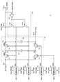
図1は、この発明の実施形態1によるチャージポンプ回路の構成を示す。このチャージポンプ回路1は、入力電圧Vinと基準電圧Vrefとの電圧差に対応する電荷を蓄積する電荷蓄積モードと、蓄積された電荷を転送する電荷転送モードとを有する。また、このチャージポンプ回路1では、出力ノードNoutにおける意図しない電圧変動に起因する過電流を抑制するための処理(過電流抑制処理)が実行される。
(Embodiment 1)
FIG. 1 shows the configuration of a charge pump circuit according to
チャージポンプ回路1は、ポンピング回路10と、駆動回路101,102,103,104と、保護回路11とを備える。なお、ここでは、チャージポンプ回路1は、正の出力電圧Voutを出力する昇圧用チャージポンプ回路であり、入力電圧Vin,基準電圧Vref,出力電圧Voutは、それぞれ、電源電圧Vdd,接地電圧Vss,入力電圧Vinの2倍の電圧値を有する電圧“2Vdd”である。
The
〔ポンピング回路〕
ポンピング回路10は、ポンピング容量C1と、出力容量C2と、駆動トランジスタT1〜T4とを含む。なお、ここでは、駆動トランジスタT1,T3,T4は、P型トランジスタであり、駆動トランジスタT2は、N型トランジスタである。
[Pumping circuit]
The
駆動トランジスタT1は、入力電圧Vinを受ける入力ノードNinとポンピング容量C1の一方端との間に接続される。駆動トランジスタT2は、ポンピング容量C1の他方端と基準電圧Vrefを受ける基準ノードNrefとの間に接続される。駆動トランジスタT3は、入力ノードNinとポンピング容量C1の他方端との間に接続される。駆動トランジスタT4は、ポンピング容量C1の一方端と出力ノードNoutとの間に接続される。出力容量C2は、出力ノードNoutと基準ノードNrefとの間に接続される。また、駆動トランジスタT1,T4のバックゲートは、それぞれ、保護抵抗R1,R4を介してポンピング容量C1の一方端,出力ノードNoutに接続される。 The drive transistor T1 is connected between an input node Nin that receives the input voltage Vin and one end of the pumping capacitor C1. The drive transistor T2 is connected between the other end of the pumping capacitor C1 and the reference node Nref that receives the reference voltage Vref. The drive transistor T3 is connected between the input node Nin and the other end of the pumping capacitor C1. The drive transistor T4 is connected between one end of the pumping capacitor C1 and the output node Nout. The output capacitor C2 is connected between the output node Nout and the reference node Nref. The back gates of the drive transistors T1 and T4 are connected to one end of the pumping capacitor C1 and the output node Nout via protective resistors R1 and R4, respectively.
〔駆動回路〕
駆動回路101は、クロック信号CK1に応答して、駆動トランジスタT1のゲートに出力電圧Voutと基準電圧Vrefとの間で振幅する制御信号Sc1を出力する。
(Drive circuit)
In response to the clock signal CK1, the
駆動回路102は、クロック信号CK1に応答して、駆動トランジスタT2のゲートに入力電圧Vinと基準電圧Vrefとの間で振幅する制御信号Sc2を出力する。
In response to the clock signal CK1, the
駆動回路103は、クロック信号CK2に応答して、駆動トランジスタT3のゲートに入力電圧Vinと基準電圧Vrefとの間で振幅する制御信号Sc3を出力する。
In response to the clock signal CK2, the
駆動回路104は、クロック信号CK2に応答して、駆動トランジスタT4のゲートに出力電圧Voutと入力電圧Vinとの間で振幅する制御信号Sc4を出力する。
In response to the clock signal CK2, the
駆動回路101〜104は、遅延回路,インバータ,レベルシフタなどを用いて構成することができる。
The
〔通常動作〕
ここで、図2を参照しつつ、図1に示したチャージポンプ回路1による通常動作について説明する。
[Normal operation]
Here, the normal operation by the
電荷蓄積期間では、クロック信号CK1は、ハイレベルからローレベルに遷移する。その遷移に応答して、駆動回路101は、制御信号Sc1をローレベル(Vss)に設定し、駆動回路102は、制御信号Sc2をハイレベル(Vdd)に設定する。これにより、駆動トランジスタT1,T2は、オフ状態からオン状態に遷移する。一方、クロック信号CK2はハイレベルのままであるので、制御信号Sc3,Sc4は、それぞれ、ハイレベル(Vdd),ハイレベル(2Vdd)のままである。そのため、駆動トランジスタT3,T4は、オフ状態のままである。その結果、ポンピング容量C1の一方端が入力ノードNinに接続されるとともにポンピング容量C1の他方端が基準ノードNrefに接続されるので、ポンピング容量C1は、入力電圧Vin(電源電圧Vdd)と基準電圧Vref(接地電圧Vss)との電圧差に対応する電荷(正電荷)を蓄積する。
In the charge accumulation period, the clock signal CK1 changes from the high level to the low level. In response to the transition, the
電荷転送期間(ここでは、昇圧期間)では、クロック信号CK1は、ハイレベルのままであるので、制御信号Sc1,Sc2は、それぞれ、ハイレベル(2Vdd),ローレベル(Vdd)のままである。そのため、駆動トランジスタT1,T2は、オフ状態のままである。一方、クロック信号CK2は、ハイレベルからローレベルへ遷移する。その遷移に応答して、駆動回路103は、制御信号Sc3をローレベル(Vss)に設定し、駆動回路104は、制御信号Sc4をローレベル(Vdd)に設定する。これにより、駆動トランジスタT3,T4は、オフ状態からオン状態へ遷移する。その結果、ポンピング容量C1の一方端が出力ノードNoutに接続されるとともにポンピング容量C1の他方端が入力ノードNinに接続されるので、ポンピング容量C1に蓄積された電荷(正電荷)が出力ノードNoutに転送され、出力ノードNoutが昇圧される。
In the charge transfer period (here, the boosting period), since the clock signal CK1 remains at the high level, the control signals Sc1 and Sc2 remain at the high level (2Vdd) and the low level (Vdd), respectively. Therefore, the drive transistors T1 and T2 remain off. On the other hand, the clock signal CK2 transits from a high level to a low level. In response to the transition, the
〔保護回路〕
図1に示した保護回路11は、出力電圧Voutを監視し、出力ノードNoutにおける電圧(出力電圧Vout)が所定の判定電圧よりも低くなると、駆動トランジスタT1,T2のそれぞれをオフ状態にする。判定電圧は、出力ノードNoutにおける意図しない電圧変動についての判定基準となる電圧(例えば、入力電圧Vinもしくは、入力電圧Vinの近傍)である。また、保護回路11は、保護トランジスタT101,T104を含む。なお、ここでは、保護トランジスタT101,T104は、P型トランジスタである。
[Protection circuit]
The
保護トランジスタT101のソースは、設定電圧Vsetを受ける設定ノードNsetに接続され、ドレインは、駆動トランジスタT101のゲートに接続され、ゲートは、出力ノードNoutに接続される。設定電圧Vsetは、駆動トランジスタT1,T2を高抵抗状態(オン状態時よりも抵抗値が高い状態、例えば、オフ状態)にするための電圧である。ここでは、設定電圧Vsetは、電源電圧Vddである。 The source of the protection transistor T101 is connected to the setting node Nset that receives the setting voltage Vset, the drain is connected to the gate of the driving transistor T101, and the gate is connected to the output node Nout. The set voltage Vset is a voltage for setting the drive transistors T1 and T2 in a high resistance state (a state in which a resistance value is higher than that in an on state, for example, an off state). Here, the set voltage Vset is the power supply voltage Vdd.
保護トランジスタT104のソースは、設定ノードNsetに接続され、ドレインは、駆動トランジスタT104のゲートに接続され、ゲートは、出力ノードNoutに接続される。 The source of the protection transistor T104 is connected to the setting node Nset, the drain is connected to the gate of the drive transistor T104, and the gate is connected to the output node Nout.
また、保護トランジスタT101,T104のバックゲートは、それぞれ、保護抵抗R101,R104を介して出力ノードNoutに接続される。 The back gates of the protection transistors T101 and T104 are connected to the output node Nout via the protection resistors R101 and R104, respectively.
〔過電流抑制処理〕
次に、図1に示した保護回路11による過電流抑制処理について説明する。ここで、保護トランジスタT101,T104の閾値電圧を“Vthp”とすると、判定電圧は、“Vdd−Vthp”になる。
[Overcurrent suppression processing]
Next, overcurrent suppression processing by the
出力ノードNoutにおける出力電圧Voutが判定電圧(Vdd−Vthp)よりも高い場合、保護トランジスタT101はオフ状態であるので、駆動トランジスタT1のゲートは、設定ノードNsetから切り離されている。そのため、駆動トランジスタT1は、制御信号Sc1に応答してオン/オフする。同様に、保護トランジスタT104もオフ状態であるので、駆動トランジスタT4は、制御信号Sc4に応答してオン/オフする。 When the output voltage Vout at the output node Nout is higher than the determination voltage (Vdd−Vthp), the protection transistor T101 is in the off state, and thus the gate of the drive transistor T1 is disconnected from the setting node Nset. Therefore, the drive transistor T1 is turned on / off in response to the control signal Sc1. Similarly, since the protection transistor T104 is also in the off state, the drive transistor T4 is turned on / off in response to the control signal Sc4.
一方、出力ノードNoutの地絡(出力ノードNoutと意図しない低電圧ノード(例えば、接地ノード)との短絡)など、出力ノードNoutにおいて意図しない電圧低下が発生して、出力電圧Voutが判定電圧(Vdd−Vthp)よりも低くなると、保護トランジスタT101がオン状態になり、駆動トランジスタT1のゲートが設定ノードNsetに接続される。これにより、駆動トランジスタT1のゲート電圧が設定電圧Vsetに固定されるので、駆動トランジスタT1は、制御信号Sc1の電圧レベルに拘わらず、強制的にオフ状態になる。同様に、保護トランジスタT104がオン状態になり、駆動トランジスタT4のゲートが設定ノードNsetに接続されるので、駆動トランジスタT4は、制御信号Sc4の電圧レベルに拘わらず、強制的にオフ状態になる。 On the other hand, an unintended voltage drop occurs at the output node Nout, such as a ground fault of the output node Nout (short circuit between the output node Nout and an unintended low voltage node (for example, a ground node)), and the output voltage Vout becomes the determination voltage ( When lower than (Vdd−Vthp), the protection transistor T101 is turned on, and the gate of the drive transistor T1 is connected to the setting node Nset. As a result, the gate voltage of the drive transistor T1 is fixed to the set voltage Vset, so that the drive transistor T1 is forcibly turned off regardless of the voltage level of the control signal Sc1. Similarly, since the protection transistor T104 is turned on and the gate of the drive transistor T4 is connected to the setting node Nset, the drive transistor T4 is forcibly turned off regardless of the voltage level of the control signal Sc4.
以上のように、出力ノードNoutにおける意図しない電圧変動(ここでは、意図しない電圧低下)が発生すると、保護回路11が駆動トランジスタT1,T4を強制的にオフ状態にする。これにより、入力ノードNinと出力ノードNoutとの間における過電流を抑制することができる。
As described above, when an unintended voltage fluctuation (in this case, an unintended voltage drop) occurs at the output node Nout, the
また、ポンピング回路10の前段に電流量を調整するための構成を設けなくても良いので、チャージポンプ回路1の昇圧効率を低下させることなく通常動作を実行することができる。
Further, since it is not necessary to provide a configuration for adjusting the amount of current in the previous stage of the
さらに、保護回路11の電流駆動能力は、駆動回路101〜104と同程度であっても良い。駆動回路101〜104の電流駆動能力は、通常、ポンピング回路10よりも小さい。このように、保護回路11の電流駆動能力は、ポンピング回路10よりも小さくても良いので、従来のように回路規模を大きくしなくても良い。そのため、チャージポンプ回路1の回路規模を低減することができる。
Furthermore, the current drive capability of the
また、駆動トランジスタT1のバックゲートとポンピング容量C1の一方端との間に保護抵抗R1を接続することにより、駆動トランジスタT1の寄生ダイオードを介して流れる過電流の電流量を少なくすることができる。同様に、駆動トランジスタT2,保護トランジスタT101,T104に対して保護抵抗R4,R101,R104がそれぞれ設けられているので、それぞれのトランジスタにおいて寄生ダイオードにおける電流量を少なくすることができる。これにより、出力電圧Voutの意図しない変動に起因する過電流をさらに抑制することができる。また、保護抵抗R1,R4,R101,R104を、それぞれ、保護トランジスタT101,T104のオン/オフに応答して動作するスイッチに置き換えた場合も、寄生ダイオードにおける電流量を少なくすることができる。 Further, by connecting the protective resistor R1 between the back gate of the drive transistor T1 and one end of the pumping capacitor C1, the amount of overcurrent flowing through the parasitic diode of the drive transistor T1 can be reduced. Similarly, since the protection resistors R4, R101, and R104 are provided for the drive transistor T2 and the protection transistors T101 and T104, the amount of current in the parasitic diode can be reduced in each transistor. Thereby, the overcurrent resulting from the unintentional fluctuation | variation of the output voltage Vout can further be suppressed. Further, when the protection resistors R1, R4, R101, and R104 are replaced with switches that operate in response to the on / off of the protection transistors T101 and T104, respectively, the amount of current in the parasitic diode can be reduced.
なお、図3のように、保護トランジスタT101,T104の接続関係を変更しても良い。図3に示した保護回路11aでは、保護トランジスタT104のソースは、保護トランジスタT101を介して設定ノードNsetに接続される。このように構成した場合も、出力ノードNoutにおいて意図しない電圧低下が発生したときに、駆動トランジスタT1,T4をオフ状態にすることができる。
As shown in FIG. 3, the connection relationship between the protection transistors T101 and T104 may be changed. In the
(実施形態2)
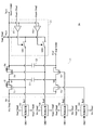
図4は、この発明の実施形態2によるチャージポンプ回路の構成を示す。このチャージポンプ回路2は、図1に示した保護回路11に代えて、保護回路21を備える。その他の構成は、図1と同様である。
(Embodiment 2)
FIG. 4 shows a configuration of a charge pump circuit according to
〔保護回路〕
保護回路21は、比較器201,204と、保護スイッチSW1,SW4とを含む。
[Protection circuit]
The
比較器201,204は、出力電圧Voutと判定電圧Vcomとを比較する。ここでは、判定電圧Vcomは、電源電圧Vddである。保護スイッチSW1は、設定ノードNsetと駆動トランジスタT1のゲートとの間に接続され、比較器201による比較結果に応答してオン/オフする。保護スイッチSW4は、設定ノードNsetと駆動トランジスタT4のゲートとの間に接続され、比較器204による比較結果に応答してオン/オフする。ここでは、スイッチSW1,SW4は、出力電圧Voutが判定電圧Vcomよりも低い場合にオン状態になる。
The
〔過電流抑制処理〕
次に、図4に示した保護回路21による過電流抑制処理について説明する。
[Overcurrent suppression processing]
Next, the overcurrent suppression process by the
出力ノードNoutにおける出力電圧Voutが判定電圧Vcom(Vdd)よりも高い場合、スイッチSW1,SW4はオフ状態であるので、駆動トランジスタT1,T4のゲートは、設定ノードNsetから切り離されている。そのため、駆動トランジスタT1,T4は、それぞれ、制御信号Sc1,Sc4に応答してオン/オフする。 When the output voltage Vout at the output node Nout is higher than the determination voltage Vcom (Vdd), since the switches SW1 and SW4 are in the off state, the gates of the drive transistors T1 and T4 are disconnected from the setting node Nset. Therefore, the drive transistors T1 and T4 are turned on / off in response to the control signals Sc1 and Sc4, respectively.
一方、出力ノードにおいて意図しない電圧低下が発生して、出力電圧Voutが判定電圧Vcom(Vdd)よりも低くなると、スイッチSW1,SW4がオン状態になり、駆動トランジスタT1,T4のゲートが設定ノードNsetに接続される。これにより、駆動トランジスタT1,T4のゲート電圧が設定電圧Vsetに固定されるので、駆動トランジスタT1,T4は、それぞれ、制御信号Sc1,Sc4の電圧レベルに拘わらず、強制的にオフ状態になる。 On the other hand, when an unintended voltage drop occurs at the output node and the output voltage Vout becomes lower than the determination voltage Vcom (Vdd), the switches SW1 and SW4 are turned on, and the gates of the drive transistors T1 and T4 are set to the setting node Nset. Connected to. As a result, the gate voltages of the drive transistors T1 and T4 are fixed to the set voltage Vset, so that the drive transistors T1 and T4 are forcibly turned off regardless of the voltage levels of the control signals Sc1 and Sc4, respectively.
以上のように、出力ノードNoutにおいて意図しない電圧変動(ここでは、意図しない電圧低下)が発生すると、保護回路21が駆動トランジスタT1,T4を強制的にオフ状態にすることにより、入力ノードNinと出力ノードNoutとの間における過電流を抑制することができる。
As described above, when an unintended voltage fluctuation (in this case, an unintended voltage drop) occurs at the output node Nout, the
また、ポンピング回路10の前段に電流量を調整するための構成を設けなくても良いので、チャージポンプ回路2の昇圧効率を低下させることなく通常動作を実行することができる。
Further, since it is not necessary to provide a configuration for adjusting the amount of current in the previous stage of the
さらに、保護回路21の電流駆動能力は、ポンピング回路10よりも小さくても良いので、従来のように回路規模を大きくしなくても良い。そのため、チャージポンプ回路2の回路規模を低減することができる。
Furthermore, since the current driving capability of the
なお、図5のように、保護回路から比較器204を取り除いても良い。図5に示した保護回路21aでは、保護スイッチSW4は、比較器201による比較結果に応答してオン/オフする。
Note that the
また、図6のように、スイッチSW1、SW4の接続関係を変更しても良い。図6に示した保護回路21bでは、スイッチSW4の一方端は、スイッチSW1を介して設定ノードNsetに接続される。このように構成した場合も、出力ノードNoutにおける出力電圧Voutが判定電圧Vcom(Vdd)よりも低いときに、駆動トランジスタT1,T4をオフ状態にすることができる。
Further, as shown in FIG. 6, the connection relationship between the switches SW1 and SW4 may be changed. In the
(降圧型チャージポンプ回路)
図7のように、実施形態1によるチャージポンプ回路は、昇圧用チャージポンプ回路としてだけでなく、降圧用チャージポンプ回路としても使用可能である。図7に示した降圧用チャージポンプ回路1aでは、駆動トランジスタT1,T3,T4は、N型トランジスタであり、駆動トランジスタT2は、P型トランジスタである。なお、図7では、入力電圧Vin,基準電圧Vrefは、それぞれ、接地電圧Vss,電源電圧Vddであり、チャージポンプ回路1aは、入力電圧Vin(Vss)から基準電圧Vref(Vdd)の分だけ降圧した負の出力電圧Vout(−Vdd)を出力する。
(Step-down charge pump circuit)
As shown in FIG. 7, the charge pump circuit according to the first embodiment can be used not only as a boost charge pump circuit but also as a step-down charge pump circuit. In the step-down
〔通常動作〕
次に、図8を参照しつつ、図7に示した降圧型チャージポンプ回路1aによる通常動作について説明する。
[Normal operation]
Next, a normal operation by the step-down
電荷蓄積期間では、クロック信号CK1は、ローレベルからハイレベルに遷移する。その遷移に応答して、駆動回路101は、制御信号Sc1をハイレベル(Vdd)に設定し、駆動回路102は、制御信号Sc2をローレベル(Vss)に設定する。これにより、駆動トランジスタT1,T2は、オフ状態からオン状態に遷移する。一方、クロック信号CK2はローレベルのままであるので、制御信号Sc3,Sc4は、それぞれ、ローレベル(Vss),ローレベル(−Vdd)のままである。そのため、駆動トランジスタT3,T4は、オフ状態のままである。その結果、ポンピング容量C1の一方端が入力ノードNinに接続されるとともにポンピング容量C1の他方端が基準ノードNrefに接続されるので、ポンピング容量C1は、電源電圧Vddと接地電圧Vssとの電圧差に対応する電荷(負電荷)を蓄積する。
In the charge accumulation period, the clock signal CK1 changes from the low level to the high level. In response to the transition, the
電荷転送期間(ここでは、降圧期間)では、クロック信号CK1は、ローレベルのままであるので、制御信号Sc1,Sc2は、それぞれ、ローレベル(−Vdd),ハイレベル(Vdd)のままである。そのため、駆動トランジスタT1,T2は、オフ状態のままである。一方、クロック信号CK2は、ローレベルからハイレベルへ遷移する。その遷移に応答して、駆動回路103は、制御信号Sc3をハイレベル(Vdd)に設定し、駆動回路104は、制御信号Sc4をハイレベル(Vss)に設定する。これにより、駆動トランジスタT3,T4は、オフ状態からオン状態へ遷移する。その結果、ポンピング容量C1の一方端が出力ノードNoutに接続されるとともにポンピング容量C1の他方端が入力ノードNinに接続されるので、ポンピング容量C1に蓄積された電荷(負電荷)が出力ノードNoutに転送される。
In the charge transfer period (here, the step-down period), since the clock signal CK1 remains at low level, the control signals Sc1 and Sc2 remain at low level (−Vdd) and high level (Vdd), respectively. . Therefore, the drive transistors T1 and T2 remain off. On the other hand, the clock signal CK2 transits from a low level to a high level. In response to the transition, the
〔保護回路〕
図7において、保護回路11は、出力ノードNoutにおける出力電圧Voutを監視し、出力電圧Voutが所定の判定電圧よりも高くなると、駆動トランジスタT1,T2のそれぞれをオフ状態にする。なお、ここでは、保護トランジスタT101,T104は、N型トランジスタであり、設定電圧Vsetは、接地電圧Vssである。
[Protection circuit]
In FIG. 7, the
〔過電流抑制動作〕
次に、図7に示した保護回路11による過電流抑制動作について説明する。ここで、保護トランジスタT101,T104の閾値電圧を“Vthn”とすると、判定電圧は、“Vss+Vthn”になる。
[Overcurrent suppression operation]
Next, the overcurrent suppressing operation by the
出力ノードにおける出力電圧Voutが判定電圧(Vss+Vthn)よりも低い場合、保護トランジスタT101はオフ状態であるので、駆動トランジスタT1のゲートは、設定ノードNsetから切り離されている。そのため、駆動トランジスタT1は、制御信号Sc1に応答してオン/オフする。同様に、保護トランジスタT104もオフ状態であるので、駆動トランジスタT4は、制御信号Sc4に応答してオン/オフする。 When the output voltage Vout at the output node is lower than the determination voltage (Vss + Vthn), the protection transistor T101 is in an off state, and thus the gate of the drive transistor T1 is disconnected from the setting node Nset. Therefore, the drive transistor T1 is turned on / off in response to the control signal Sc1. Similarly, since the protection transistor T104 is also in the off state, the drive transistor T4 is turned on / off in response to the control signal Sc4.
一方、出力ノードNoutの天絡(出力ノードNoutと意図しない高電圧ノード(例えば、電源ノード)との短絡)など、出力ノードNoutにおいて意図しない電圧上昇が発生して、出力電圧Voutが判定電圧(Vss+Vthn)よりも高くなると、保護トランジスタT101がオン状態になり、駆動トランジスタT1のゲートが設定ノードNsetに接続される。これにより、駆動トランジスタT1のゲート電圧が設定電圧Vsetに固定されるので、駆動トランジスタT1は、制御信号Sc1の電圧レベルに拘わらず、強制的にオフ状態になる。同様に、保護トランジスタT104がオン状態になり、駆動トランジスタT4のゲートが設定ノードNsetに接続されるので、駆動トランジスタT4は、制御信号Sc4の電圧レベルに拘わらず、強制的にオフ状態になる。 On the other hand, an unintentional voltage rise occurs at the output node Nout, such as a power supply fault of the output node Nout (short circuit between the output node Nout and an unintended high voltage node (for example, a power supply node)), and the output voltage Vout becomes the determination voltage ( When it becomes higher than (Vss + Vthn), the protection transistor T101 is turned on, and the gate of the drive transistor T1 is connected to the setting node Nset. As a result, the gate voltage of the drive transistor T1 is fixed to the set voltage Vset, so that the drive transistor T1 is forcibly turned off regardless of the voltage level of the control signal Sc1. Similarly, since the protection transistor T104 is turned on and the gate of the drive transistor T4 is connected to the setting node Nset, the drive transistor T4 is forcibly turned off regardless of the voltage level of the control signal Sc4.
以上のように、出力ノードNoutにおいて意図しない電圧変動(ここでは、意図しない電圧上昇)が発生すると、保護回路11が駆動トランジスタT1,T4を強制的にオフ状態にする。これにより、入力ノードNinと出力ノードNoutとの間における過電流を抑制することができる。
As described above, when an unintended voltage fluctuation (unintentional voltage increase in this case) occurs at the output node Nout, the
なお、図9のように、実施形態2に示したチャージポンプ回路も降圧用チャージポンプ回路として使用することができる。図9に示したチャージポンプ回路2aでは、スイッチSW1,SW4は、出力電圧Voutが判定電圧Vcomよりも高い場合にオン状態になる。ここでは、判定電圧Vcomは、接地電圧Vssである。
As shown in FIG. 9, the charge pump circuit shown in
次に、図9に示した保護回路21による過電流抑制処理について説明する。
Next, the overcurrent suppression process by the
出力ノードNoutにおける出力電圧Voutが判定電圧Vcom(Vss)よりも低い場合、スイッチSW1,SW4はオフ状態であるので、駆動トランジスタT1,T4のゲートは、設定ノードNsetから切り離されている。そのため、駆動トランジスタT1,T4は、それぞれ、制御信号Sc1,Sc4に応答してオン/オフする。 When the output voltage Vout at the output node Nout is lower than the determination voltage Vcom (Vss), the switches SW1 and SW4 are in the off state, so that the gates of the drive transistors T1 and T4 are disconnected from the setting node Nset. Therefore, the drive transistors T1 and T4 are turned on / off in response to the control signals Sc1 and Sc4, respectively.
一方、出力ノードNoutにおいて意図しない電圧上昇が発生して、出力電圧Voutが判定電圧Vcom(Vss)よりも高くなると、スイッチSW1,SW4がオン状態になり、駆動トランジスタT1,T4のゲートが設定ノードNsetに接続される。これにより、駆動トランジスタT1,T4のゲート電圧が設定電圧Vsetに固定されるので、駆動トランジスタT1,T4は、それぞれ、制御信号Sc1,Sc4の電圧レベルに拘わらず、強制的にオフ状態になる。 On the other hand, when an unintended voltage rise occurs at the output node Nout and the output voltage Vout becomes higher than the determination voltage Vcom (Vss), the switches SW1 and SW4 are turned on, and the gates of the drive transistors T1 and T4 are set to the setting node. Connected to Nset. As a result, the gate voltages of the drive transistors T1 and T4 are fixed to the set voltage Vset, so that the drive transistors T1 and T4 are forcibly turned off regardless of the voltage levels of the control signals Sc1 and Sc4, respectively.
以上のように、出力ノードNoutにおいて意図しない電圧変動(ここでは、意図しない電圧上昇)が発生すると、保護回路21が駆動トランジスタT1,T4が強制的にオフ状態にすることにより、入力ノードNinと出力ノードNoutとの間における過電流を抑制することができる。
As described above, when an unintended voltage fluctuation (in this case, an unintended voltage increase) occurs at the output node Nout, the
(その他の実施形態)
以上の各実施形態において、保護回路は、2つの駆動トランジスタT1,T4に対応する2つの保護トランジスタT101,T104(または、2つのスイッチSW1,SW4)を含んでいるが、少なくとも一方の保護トランジスタ(または、少なくとも一方のスイッチ)を含んでいれば、意図しない電圧変動に起因する過電流を抑制することが可能である。
(Other embodiments)
In each of the above embodiments, the protection circuit includes two protection transistors T101 and T104 (or two switches SW1 and SW4) corresponding to the two drive transistors T1 and T4, but at least one of the protection transistors ( If at least one of the switches is included, overcurrent caused by unintended voltage fluctuation can be suppressed.
また、駆動トランジスタT1,T4に同一の設定電圧Vsetを供給するものとして説明したが、駆動トランジスタT1,T4にそれぞれ異なる設定電圧Vsetを供給しても良い。また、設定電圧Vsetが入力電圧Vinと同一である場合、設定ノードNsetは、入力ノードNinであっても良い。例えば、図1に示したチャージポンプ回路1において、保護トランジスタT101,T104のソースを入力ノードNinに接続しても良い。
Although the description has been given assuming that the same set voltage Vset is supplied to the drive transistors T1 and T4, different set voltages Vset may be supplied to the drive transistors T1 and T4. When the set voltage Vset is the same as the input voltage Vin, the set node Nset may be the input node Nin. For example, in the
以上のように、この発明によるチャージポンプ回路は、昇圧効率(または降圧効率)を低下させることなく過電流を抑制することができるので、携帯電話,デジタルビデオカメラ,デジタルスチールカメラなどの電子機器の電源回路などとして有用である。 As described above, the charge pump circuit according to the present invention can suppress overcurrent without lowering the step-up efficiency (or step-down efficiency). Therefore, the charge pump circuit of the electronic device such as a mobile phone, a digital video camera, or a digital still camera can be used. It is useful as a power supply circuit.
1,2 昇圧型チャージポンプ回路
1a,2a 降圧型チャージポンプ回路
10 ポンピング回路
101,102,103,104 駆動回路
11,11a,21,21a,21b 保護回路
C1 ポンピング容量
C2 出力容量
T1,T2,T3,T4 駆動トランジスタ
T101,T104 保護トランジスタ
R1,R4,R101,R104 保護抵抗
201,204 比較器
SW1,SW4 保護スイッチ
1, 2 Step-up
Claims (9)
ポンピング容量と、前記入力電圧を受ける入力ノードと前記ポンピング容量の一方端との間に接続される第1の駆動トランジスタと、前記出力電圧を出力するための出力ノードと前記ポンピング容量の一方端との間に接続される第2の駆動トランジスタとを含み、電荷蓄積モードにおいて前記第1の駆動トランジスタをオン状態にして前記ポンピング容量に電荷を蓄積する一方、電荷転送モードにおいて前記第2の駆動トランジスタをオン状態にして前記ポンピング容量に蓄積された電荷を前記出力ノードへ転送するポンピング回路と、
所定の判定電圧と前記出力電圧との高低関係に基づいて、前記第1および第2の駆動トランジスタの少なくとも1つを前記オン状態時よりも抵抗値が高い高抵抗状態に設定する保護回路とを備える
ことを特徴とするチャージポンプ回路。 A circuit that boosts or steps down an input voltage and outputs an output voltage,
A pumping capacitor; a first driving transistor connected between an input node receiving the input voltage and one end of the pumping capacitor; an output node for outputting the output voltage; and one end of the pumping capacitor A second driving transistor connected between the first driving transistor and the second driving transistor in the charge transfer mode while the first driving transistor is turned on to store the charge in the pumping capacitor. A pumping circuit for turning on the charge and transferring the charge accumulated in the pumping capacitor to the output node;
A protection circuit configured to set at least one of the first and second drive transistors in a high resistance state having a higher resistance value than that in the on state based on a level relationship between a predetermined determination voltage and the output voltage. A charge pump circuit comprising:
前記保護回路は、
前記第1の駆動トランジスタを高抵抗状態に設定するための第1の設定電圧を受ける第1の設定ノードに接続されるソースと、前記出力ノードに接続されるゲートと、前記第1の駆動トランジスタのゲートに接続されるドレインとを有する第1の保護トランジスタを含む
ことを特徴とするチャージポンプ回路。 In claim 1,
The protection circuit is
A source connected to a first setting node for receiving a first setting voltage for setting the first driving transistor in a high resistance state; a gate connected to the output node; and the first driving transistor And a first protection transistor having a drain connected to the gate of the charge pump circuit.
前記保護回路は、
前記第2の駆動トランジスタを高抵抗状態に設定するための第2の設定電圧を受ける第2の設定ノードに接続されるソースと、前記出力ノードに接続されるゲートと、前記第2の駆動トランジスタのゲートに接続されるドレインとを有する第2の保護トランジスタを含む
ことを特徴とするチャージポンプ回路。 In claim 1 or claim 2,
The protection circuit is
A source connected to a second setting node for receiving a second setting voltage for setting the second driving transistor in a high resistance state; a gate connected to the output node; and the second driving transistor And a second protection transistor having a drain connected to the gate of the charge pump circuit.
前記保護回路は、
前記出力ノードにおける出力電圧と前記判定電圧とを比較する第1の比較回路と、
前記第1の駆動トランジスタを高抵抗状態にするための第1の設定ノードと前記第1の駆動トランジスタのゲートとの間に接続され、前記第1の比較回路による比較結果に応答してオン/オフする第1の保護スイッチとを含む
ことを特徴とするチャージポンプ回路。 In claim 1,
The protection circuit is
A first comparison circuit for comparing an output voltage at the output node with the determination voltage;
Connected between a first setting node for bringing the first driving transistor into a high resistance state and a gate of the first driving transistor, and turned on / off in response to a comparison result by the first comparison circuit. A charge pump circuit comprising: a first protection switch that is turned off.
前記保護回路は、
前記出力ノードにおける出力電圧と前記判定電圧とを比較する第2の比較回路と、
前記第2の駆動トランジスタを高抵抗状態にするための第2の設定ノードと前記第2の駆動トランジスタのゲートとの間に接続され、前記第2の比較回路による比較結果に応答してオン/オフする第2の保護スイッチとを含む
ことを特徴とするチャージポンプ回路。 In claim 1 or claim 4,
The protection circuit is
A second comparison circuit for comparing the output voltage at the output node with the determination voltage;
The second driving transistor is connected between a second setting node for bringing the second driving transistor into a high resistance state and a gate of the second driving transistor, and is turned on / off in response to a comparison result by the second comparison circuit. A charge pump circuit comprising: a second protection switch that is turned off.
前記保護回路は、
前記第2の駆動トランジスタを高抵抗状態にするための第2の設定ノードと前記第2の駆動トランジスタのゲートとの間に接続され、前記第1の比較回路による比較結果に応答してオン/オフする第2の保護スイッチをさらに含む
ことを特徴とするチャージポンプ回路。 In claim 4,
The protection circuit is
The second driving transistor is connected between a second setting node for bringing the second driving transistor into a high resistance state and a gate of the second driving transistor, and is turned on / off in response to a comparison result by the first comparison circuit. A charge pump circuit further comprising a second protection switch to be turned off.
前記第1の設定ノードは、前記入力ノードである
ことを特徴とするチャージポンプ回路。 In claim 2 or claim 4,
The charge pump circuit according to claim 1, wherein the first setting node is the input node.
前記第2の設定ノードは、前記入力ノードである
ことを特徴とするチャージポンプ回路。 In any one of Claims 3, 5, and 6,
The charge pump circuit according to claim 2, wherein the second setting node is the input node.
ことを特徴とする電子機器。 An electronic apparatus comprising the charge pump circuit according to claim 1.
Priority Applications (2)
| Application Number | Priority Date | Filing Date | Title |
|---|---|---|---|
| JP2008021475A JP2009183111A (en) | 2008-01-31 | 2008-01-31 | Charge pump circuit and electronic device including the same |
| US12/265,189 US7944276B2 (en) | 2008-01-31 | 2008-11-05 | Charge pump circuit and electronic apparatus provided with the same |
Applications Claiming Priority (1)
| Application Number | Priority Date | Filing Date | Title |
|---|---|---|---|
| JP2008021475A JP2009183111A (en) | 2008-01-31 | 2008-01-31 | Charge pump circuit and electronic device including the same |
Publications (1)
| Publication Number | Publication Date |
|---|---|
| JP2009183111A true JP2009183111A (en) | 2009-08-13 |
Family
ID=40931083
Family Applications (1)
| Application Number | Title | Priority Date | Filing Date |
|---|---|---|---|
| JP2008021475A Pending JP2009183111A (en) | 2008-01-31 | 2008-01-31 | Charge pump circuit and electronic device including the same |
Country Status (2)
| Country | Link |
|---|---|
| US (1) | US7944276B2 (en) |
| JP (1) | JP2009183111A (en) |
Cited By (3)
| Publication number | Priority date | Publication date | Assignee | Title |
|---|---|---|---|---|
| WO2020136820A1 (en) * | 2018-12-27 | 2020-07-02 | 三菱電機株式会社 | Charge pump circuit and semiconductor device |
| WO2020136821A1 (en) * | 2018-12-27 | 2020-07-02 | 三菱電機株式会社 | Charge pump circuit and semiconductor device |
| JP2022006505A (en) * | 2020-06-24 | 2022-01-13 | 旭化成エレクトロニクス株式会社 | Charge pump device |
Families Citing this family (18)
| Publication number | Priority date | Publication date | Assignee | Title |
|---|---|---|---|---|
| US8115597B1 (en) * | 2007-03-07 | 2012-02-14 | Impinj, Inc. | RFID tags with synchronous power rectifier |
| US7671665B2 (en) * | 2008-07-01 | 2010-03-02 | Hamilton Sundstrand Corporation | Constant-ON state high side switch circuit |
| JP5300001B2 (en) * | 2008-10-07 | 2013-09-25 | ルネサスエレクトロニクス株式会社 | Boost circuit and semiconductor integrated circuit device |
| TW201105015A (en) * | 2009-07-22 | 2011-02-01 | Green Solution Tech Co Ltd | Charge pump circuit |
| US8330509B2 (en) * | 2010-04-12 | 2012-12-11 | Intel Mobile Communications GmbH | Suppression of low-frequency noise from phase detector in phase control loop |
| KR101556838B1 (en) | 2011-05-05 | 2015-10-13 | 아크틱 샌드 테크놀로지스, 인크. | Dc-dc converter with modular stages |
| US10680515B2 (en) | 2011-05-05 | 2020-06-09 | Psemi Corporation | Power converters with modular stages |
| JP6042091B2 (en) * | 2011-05-13 | 2016-12-14 | ローム株式会社 | Switching regulator control circuit, switching regulator and electronic equipment, switching power supply, television |
| US8743553B2 (en) | 2011-10-18 | 2014-06-03 | Arctic Sand Technologies, Inc. | Power converters with integrated capacitors |
| US8723491B2 (en) | 2011-12-19 | 2014-05-13 | Arctic Sand Technologies, Inc. | Control of power converters with capacitive energy transfer |
| US8724353B1 (en) | 2013-03-15 | 2014-05-13 | Arctic Sand Technologies, Inc. | Efficient gate drivers for switched capacitor converters |
| US9203299B2 (en) | 2013-03-15 | 2015-12-01 | Artic Sand Technologies, Inc. | Controller-driven reconfiguration of switched-capacitor power converter |
| US8619445B1 (en) | 2013-03-15 | 2013-12-31 | Arctic Sand Technologies, Inc. | Protection of switched capacitor power converter |
| US9847712B2 (en) * | 2013-03-15 | 2017-12-19 | Peregrine Semiconductor Corporation | Fault control for switched capacitor power converter |
| TW201640796A (en) | 2015-03-13 | 2016-11-16 | 亞提克聖德技術股份有限公司 | DC-to-DC transformer with inductor for promoting energy transfer between capacitors |
| WO2017007991A1 (en) | 2015-07-08 | 2017-01-12 | Arctic Sand Technologies, Inc. | Switched-capacitor power converters |
| US11489441B2 (en) * | 2020-06-02 | 2022-11-01 | Texas Instruments Incorporated | Reference voltage generation circuits and related methods |
| US12525816B2 (en) * | 2021-03-24 | 2026-01-13 | Psemi Corporation | Power converters and methods for protecting power converters |
Citations (2)
| Publication number | Priority date | Publication date | Assignee | Title |
|---|---|---|---|---|
| JPS63217971A (en) * | 1987-03-04 | 1988-09-12 | Fuji Electric Co Ltd | Voltage multiplier |
| US6320797B1 (en) * | 1999-02-24 | 2001-11-20 | Micron Technology, Inc. | Method and circuit for regulating the output voltage from a charge pump circuit, and memory device using same |
Family Cites Families (15)
| Publication number | Priority date | Publication date | Assignee | Title |
|---|---|---|---|---|
| US5081371A (en) * | 1990-11-07 | 1992-01-14 | U.S. Philips Corp. | Integrated charge pump circuit with back bias voltage reduction |
| AU5165798A (en) * | 1996-11-05 | 1998-05-29 | Aplus Flash Technology, Inc. | Positive/negative high voltage charge pump system |
| US6310789B1 (en) | 1999-06-25 | 2001-10-30 | The Procter & Gamble Company | Dynamically-controlled, intrinsically regulated charge pump power converter |
| KR100383769B1 (en) * | 2000-12-18 | 2003-05-14 | 주식회사 하이닉스반도체 | Pumping voltage regulation circuit |
| US6734718B1 (en) * | 2002-12-23 | 2004-05-11 | Sandisk Corporation | High voltage ripple reduction |
| JP4181441B2 (en) | 2003-04-14 | 2008-11-12 | 株式会社リコー | DC-DC converter |
| JP4308158B2 (en) | 2004-03-30 | 2009-08-05 | ローム株式会社 | Boost control device and electronic device using the same |
| JP4024814B2 (en) * | 2005-02-24 | 2007-12-19 | シャープ株式会社 | Charge pump type DC / DC converter circuit |
| US7271642B2 (en) * | 2005-12-27 | 2007-09-18 | Aimtron Technology Corp. | Charge pump drive circuit for a light emitting diode |
| US7250810B1 (en) * | 2005-12-27 | 2007-07-31 | Aimtron Technology Corp. | Multi-mode charge pump drive circuit with improved input noise at a moment of mode change |
| US7554385B2 (en) * | 2006-01-27 | 2009-06-30 | Rohm Co., Ltd. | Charge pump circuit and electric appliance therewith |
| JP2008029098A (en) * | 2006-07-20 | 2008-02-07 | Oki Electric Ind Co Ltd | Voltage booster circuit |
| DE102006046387B4 (en) * | 2006-09-29 | 2015-11-19 | Texas Instruments Deutschland Gmbh | DC-DC boost converter with a charge pump |
| KR100818710B1 (en) * | 2006-11-21 | 2008-04-01 | 주식회사 하이닉스반도체 | Voltage pumping device |
| JP5078464B2 (en) * | 2007-06-29 | 2012-11-21 | 株式会社リコー | Charge pump circuit |
-
2008
- 2008-01-31 JP JP2008021475A patent/JP2009183111A/en active Pending
- 2008-11-05 US US12/265,189 patent/US7944276B2/en not_active Expired - Fee Related
Patent Citations (2)
| Publication number | Priority date | Publication date | Assignee | Title |
|---|---|---|---|---|
| JPS63217971A (en) * | 1987-03-04 | 1988-09-12 | Fuji Electric Co Ltd | Voltage multiplier |
| US6320797B1 (en) * | 1999-02-24 | 2001-11-20 | Micron Technology, Inc. | Method and circuit for regulating the output voltage from a charge pump circuit, and memory device using same |
Cited By (8)
| Publication number | Priority date | Publication date | Assignee | Title |
|---|---|---|---|---|
| WO2020136820A1 (en) * | 2018-12-27 | 2020-07-02 | 三菱電機株式会社 | Charge pump circuit and semiconductor device |
| WO2020136821A1 (en) * | 2018-12-27 | 2020-07-02 | 三菱電機株式会社 | Charge pump circuit and semiconductor device |
| JPWO2020136820A1 (en) * | 2018-12-27 | 2021-09-27 | 三菱電機株式会社 | Charge pump circuit and semiconductor device |
| JPWO2020136821A1 (en) * | 2018-12-27 | 2021-09-27 | 三菱電機株式会社 | Charge pump circuit and semiconductor device |
| JP7134255B2 (en) | 2018-12-27 | 2022-09-09 | 三菱電機株式会社 | Charge pump circuit and semiconductor device |
| JP7191124B2 (en) | 2018-12-27 | 2022-12-16 | 三菱電機株式会社 | Charge pump circuit and semiconductor device |
| JP2022006505A (en) * | 2020-06-24 | 2022-01-13 | 旭化成エレクトロニクス株式会社 | Charge pump device |
| JP7438037B2 (en) | 2020-06-24 | 2024-02-26 | 旭化成エレクトロニクス株式会社 | charge pump device |
Also Published As
| Publication number | Publication date |
|---|---|
| US7944276B2 (en) | 2011-05-17 |
| US20090195298A1 (en) | 2009-08-06 |
Similar Documents
| Publication | Publication Date | Title |
|---|---|---|
| JP2009183111A (en) | Charge pump circuit and electronic device including the same | |
| US7405549B2 (en) | Soft start circuit, power supply unit and electric equipment | |
| JP4870058B2 (en) | Constant current drive circuit | |
| JP5554910B2 (en) | Control circuit for charge pump circuit and power supply circuit using them | |
| JP4666345B2 (en) | Charge pump circuit | |
| JP5228971B2 (en) | Power circuit | |
| US8638389B2 (en) | Power supply circuit, integrated circuit device, solid-state imaging apparatus, and electronic apparatus | |
| JP4781744B2 (en) | POWER SUPPLY DEVICE AND ELECTRIC DEVICE USING THE SAME | |
| JP2006006004A (en) | Buck-boost DC-DC converter | |
| JP2010051079A (en) | Dc-dc converter and control method | |
| CN104065263A (en) | Voltage Conversion Circuit And Switching Control Circuit | |
| JP5865028B2 (en) | DC-DC converter | |
| JP2012044784A (en) | Switching power supply device | |
| CN102594130A (en) | Method for outputting constant difference voltage and charge pump circuit | |
| JP2018057072A (en) | Signal output circuit | |
| JP5091101B2 (en) | Soft start circuit and power supply circuit including the soft start circuit | |
| JP2009081984A (en) | Charge pump circuit | |
| JP2011067025A (en) | Dc-dc converter | |
| JP4974520B2 (en) | Charge pump circuit, LCD driver IC, electronic equipment | |
| JP2007151246A (en) | Dc/dc converter | |
| JPWO2006085632A1 (en) | Power supply circuit and portable device | |
| JP2009169749A (en) | Soft start circuit | |
| JP4808995B2 (en) | Semiconductor circuit device | |
| JP2006129127A (en) | Voltage supply circuit and solid-state imaging device using the same | |
| JP4400145B2 (en) | Power supply |
Legal Events
| Date | Code | Title | Description |
|---|---|---|---|
| A621 | Written request for application examination |
Free format text: JAPANESE INTERMEDIATE CODE: A621 Effective date: 20100831 |
|
| RD02 | Notification of acceptance of power of attorney |
Free format text: JAPANESE INTERMEDIATE CODE: A7422 Effective date: 20120130 |
|
| A977 | Report on retrieval |
Free format text: JAPANESE INTERMEDIATE CODE: A971007 Effective date: 20120516 |
|
| A131 | Notification of reasons for refusal |
Free format text: JAPANESE INTERMEDIATE CODE: A131 Effective date: 20120522 |
|
| A02 | Decision of refusal |
Free format text: JAPANESE INTERMEDIATE CODE: A02 Effective date: 20120925 |