JP2009192572A - Liquid crystal display device and inspection method thereof - Google Patents
Liquid crystal display device and inspection method thereof Download PDFInfo
- Publication number
- JP2009192572A JP2009192572A JP2008030100A JP2008030100A JP2009192572A JP 2009192572 A JP2009192572 A JP 2009192572A JP 2008030100 A JP2008030100 A JP 2008030100A JP 2008030100 A JP2008030100 A JP 2008030100A JP 2009192572 A JP2009192572 A JP 2009192572A
- Authority
- JP
- Japan
- Prior art keywords
- wiring
- liquid crystal
- conductive pattern
- crystal display
- measurement
- Prior art date
- Legal status (The legal status is an assumption and is not a legal conclusion. Google has not performed a legal analysis and makes no representation as to the accuracy of the status listed.)
- Pending
Links
Images





Classifications
-
- G—PHYSICS
- G02—OPTICS
- G02F—OPTICAL DEVICES OR ARRANGEMENTS FOR THE CONTROL OF LIGHT BY MODIFICATION OF THE OPTICAL PROPERTIES OF THE MEDIA OF THE ELEMENTS INVOLVED THEREIN; NON-LINEAR OPTICS; FREQUENCY-CHANGING OF LIGHT; OPTICAL LOGIC ELEMENTS; OPTICAL ANALOGUE/DIGITAL CONVERTERS
- G02F1/00—Devices or arrangements for the control of the intensity, colour, phase, polarisation or direction of light arriving from an independent light source, e.g. switching, gating or modulating; Non-linear optics
- G02F1/01—Devices or arrangements for the control of the intensity, colour, phase, polarisation or direction of light arriving from an independent light source, e.g. switching, gating or modulating; Non-linear optics for the control of the intensity, phase, polarisation or colour
- G02F1/13—Devices or arrangements for the control of the intensity, colour, phase, polarisation or direction of light arriving from an independent light source, e.g. switching, gating or modulating; Non-linear optics for the control of the intensity, phase, polarisation or colour based on liquid crystals, e.g. single liquid crystal display cells
- G02F1/133—Constructional arrangements; Operation of liquid crystal cells; Circuit arrangements
- G02F1/1333—Constructional arrangements; Manufacturing methods
- G02F1/1345—Conductors connecting electrodes to cell terminals
-
- G—PHYSICS
- G02—OPTICS
- G02F—OPTICAL DEVICES OR ARRANGEMENTS FOR THE CONTROL OF LIGHT BY MODIFICATION OF THE OPTICAL PROPERTIES OF THE MEDIA OF THE ELEMENTS INVOLVED THEREIN; NON-LINEAR OPTICS; FREQUENCY-CHANGING OF LIGHT; OPTICAL LOGIC ELEMENTS; OPTICAL ANALOGUE/DIGITAL CONVERTERS
- G02F1/00—Devices or arrangements for the control of the intensity, colour, phase, polarisation or direction of light arriving from an independent light source, e.g. switching, gating or modulating; Non-linear optics
- G02F1/01—Devices or arrangements for the control of the intensity, colour, phase, polarisation or direction of light arriving from an independent light source, e.g. switching, gating or modulating; Non-linear optics for the control of the intensity, phase, polarisation or colour
- G02F1/13—Devices or arrangements for the control of the intensity, colour, phase, polarisation or direction of light arriving from an independent light source, e.g. switching, gating or modulating; Non-linear optics for the control of the intensity, phase, polarisation or colour based on liquid crystals, e.g. single liquid crystal display cells
- G02F1/133—Constructional arrangements; Operation of liquid crystal cells; Circuit arrangements
- G02F1/136—Liquid crystal cells structurally associated with a semi-conducting layer or substrate, e.g. cells forming part of an integrated circuit
- G02F1/1362—Active matrix addressed cells
- G02F1/136254—Checking; Testing
Landscapes
- Physics & Mathematics (AREA)
- Nonlinear Science (AREA)
- Mathematical Physics (AREA)
- Chemical & Material Sciences (AREA)
- Crystallography & Structural Chemistry (AREA)
- General Physics & Mathematics (AREA)
- Optics & Photonics (AREA)
- Liquid Crystal (AREA)
- Devices For Indicating Variable Information By Combining Individual Elements (AREA)
- Testing Electric Properties And Detecting Electric Faults (AREA)
Abstract
【課題】導電性パターン部を小さくすることなく、近年のドライバーLSIのバンプ間の狭ピッチ化に対応可能な液晶表示装置およびその検査方法を提供することを目的とする。
【解決手段】本発明に係る液晶表示装置は、複数の液晶表示素子が形成された表示部21と、表示部21の電極基板1に形成され、複数の液晶表示素子に信号を供給する複数の配線3a−1,3a−2とを備える。そして、電極基板1の周縁部に設けられ、複数の配線3a−1,3a−2の電極端子と接続するドライバーLSI6と、表示部21とドライバーLSI6との間に位置する各複数の配線3a−1,3a−2を分岐してなる測定配線4−1,4−2とを備える。そして、分岐点を除く測定配線4−1,4−2上に第1の絶縁層を介して形成され、各複数の配線3a−1,3a−2から分岐した測定配線4−1,4−2同士にまたがって形成される導電性パターン部7とを備える。
【選択図】図1An object of the present invention is to provide a liquid crystal display device and an inspection method thereof that can cope with a narrow pitch between bumps of a driver LSI in recent years without reducing a conductive pattern portion.
A liquid crystal display device according to the present invention includes a display unit 21 on which a plurality of liquid crystal display elements are formed, and a plurality of electrodes that are formed on an electrode substrate 1 of the display unit 21 and supply signals to the plurality of liquid crystal display elements. Wirings 3a-1 and 3a-2 are provided. The driver LSI 6 provided on the peripheral portion of the electrode substrate 1 and connected to the electrode terminals of the plurality of wirings 3a-1 and 3a-2, and the plurality of wirings 3a- positioned between the display unit 21 and the driver LSI 6 are provided. 1 and 3a-2, and measurement wirings 4-1 and 4-2. Then, the measurement wires 4-1 and 4-2, which are formed on the measurement wires 4-1 and 4-2 excluding the branch points via the first insulating layer, are branched from the plurality of wires 3a-1 and 3a-2. And a conductive pattern portion 7 formed across the two.
[Selection] Figure 1
Description
本発明は、液晶表示装置およびその検査方法に関する発明であって、特に、表示素子を駆動するためのドライバーLSI(Large Scale Integration)が設けられた液晶表示装置およびその検査方法に関するものである。 The present invention relates to a liquid crystal display device and an inspection method thereof, and more particularly to a liquid crystal display device provided with a driver LSI (Large Scale Integration) for driving a display element and an inspection method thereof.
小型化、低コスト化の観点から、液晶表示装置では、ドライバーLSIのバンプを、ガラス基板上に設けられた配線の電極端子に直接接続させるCOG(Chip On Glass)方式を採用する場合が多い。このCOG方式を含め、液晶表示装置では、線欠陥等の表示不良が生じた場合、ドライバーLSIおよび配線のいずれに原因があるかを区別する必要があった。 From the viewpoint of miniaturization and cost reduction, a liquid crystal display device often adopts a COG (Chip On Glass) method in which bumps of a driver LSI are directly connected to electrode terminals of wirings provided on a glass substrate. In the liquid crystal display device including this COG method, when a display defect such as a line defect occurs, it is necessary to distinguish between the driver LSI and the wiring.
しかし、配線は、ドライバーLSIのバンプと接続する端子以外は絶縁層に覆われているため、表示不良の究明を容易に行うことができなかった。その問題を解決する手段として、特許文献1に開示されているような手段が提案されている。この特許文献1の液晶表示装置では、ドライバーLSIと表示素子との間の配線に、幅の広いパターン形状からなる測定パターン部と、その測定パターン部上に導電性パターン部を設けている。そして、欠陥検査時に、測定パターン部と導電性パターン部とをレーザー照射により接続させ、その導電性パターン部に測定器を接続することにより、ドライバーLSIからの出力、例えば、出力信号や出力波形を確認し、表示不良の究明を行っていた。
However, since the wiring is covered with an insulating layer except for the terminals connected to the bumps of the driver LSI, it has not been possible to easily investigate display defects. As means for solving the problem, means as disclosed in
特許文献1に記載された接続形態では、複数の配線の不具合を配線ごとに確認することを考慮して、測定パターン部および導電性パターン部を配線ごとに個別に配置している。その一方で、近年、ドライバーLSIの小型化および多出力化に伴い、出力バンプ間のピッチを狭くすることが求められている。しかしながら、レーザー照射により確実に接続して、ドライバーLSIからの出力を測定可能にするためには、ある程度の大きさの測定パターン部および導電性パターン部を配置する必要がある。それにも関わらず、このような測定パターン部および導電性パターン部を配線ごとに個別に配置すると、配線間のピッチを狭くすることができないため、バンプ間のピッチを狭くすることができないという問題があった。
In the connection form described in
本発明は、上記のような問題点を解決するためになされたものであり、導電性パターン部を小さくすることなく、近年のドライバーLSIのバンプ間の狭ピッチ化に対応可能な液晶表示装置、および、液晶表示装置の検査方法を提供することを目的とする。 The present invention has been made to solve the above-described problems, and a liquid crystal display device that can cope with a narrow pitch between bumps of a driver LSI in recent years without reducing the conductive pattern portion, And it aims at providing the inspection method of a liquid crystal display device.
本発明に係る液晶表示装置は、相対向する二枚の絶縁性基板によって液晶層を挟持してなり、複数の表示素子が形成された表示部と、前記絶縁性基板の少なくとも一方に形成され、前記複数の表示素子に信号を供給する複数の配線とを備える。そして、前記絶縁性基板の周縁部に設けられ、前記複数の配線の端子と接続することで前記複数の表示素子を駆動するドライバーLSIと、前記表示部と前記ドライバーLSIとの間に位置する各前記複数の配線を分岐してなる測定配線とを備える。そして、分岐点を除く前記測定配線上に第1の絶縁層を介して形成され、各前記複数の配線から分岐した前記測定配線同士にまたがって形成される導電性パターン部を備える。 The liquid crystal display device according to the present invention has a liquid crystal layer sandwiched between two insulating substrates facing each other, and is formed on at least one of a display portion in which a plurality of display elements are formed and the insulating substrate, And a plurality of wirings for supplying signals to the plurality of display elements. A driver LSI that is provided at a peripheral portion of the insulating substrate and that drives the plurality of display elements by being connected to terminals of the plurality of wirings; and each of the driver LSIs that is positioned between the display unit and the driver LSI. A measurement wiring formed by branching the plurality of wirings. And the electroconductive pattern part formed over the said measurement wiring branched from each said some wiring is formed on the said measurement wiring except a branch point via a 1st insulating layer.
本発明の液晶表示装置によれば、複数の配線が導電性パターン部を共有するため、導電性パターン部の数を削減することができる。これにより、導電性パターン部を小さくすることなく、配線間のピッチを狭くすることができ、その結果、ドライバーLSIのバンプ間のピッチを狭くすることができる。 According to the liquid crystal display device of the present invention, since the plurality of wirings share the conductive pattern portion, the number of conductive pattern portions can be reduced. Thereby, the pitch between wirings can be narrowed without reducing the conductive pattern portion, and as a result, the pitch between bumps of the driver LSI can be narrowed.
<実施の形態1>
図1は、本実施の形態に係る液晶表示装置が備える表示部21と電極端子部22とを示す平面図である。まず、表示部21の構造について説明する。表示部21は、相対向する二枚の絶縁性基板(例えばガラス基板)である電極基板1と対向基板2とによって液晶層を挟持してなり、複数の表示素子である液晶表示素子が形成される。本実施の形態では、電極基板1は、対向基板2から外側(図1の下側)に張り出している。なお、図示していないが、表示部21の電極基板1上には、複数のゲート配線および複数のソース配線が設けられており、これらの交差部付近には、スイッチング素子である薄膜トランジスタが配置されている。そして、この薄膜トランジスタに接続された画素電極等がマトリックス状に配置されている(いずれも図示せず)。
<
FIG. 1 is a plan view showing a
表示部21の対向基板2上には、透明導電膜よりなる対向電極、カラー表示用の着色フィルタ層および各画素間に配置されたブラックマトリックス等が形成されている(いずれも図示せず)。表示部21の電極基板1と対向基板2とは、液晶層およびスペーサーを介して重ね合わされ、シール材により封止されている。
On the
次に、電極端子部22の構成について説明する。本実施の形態では、電極端子部22は、対向基板2から外側に張り出した電極基板1上(以下、電極基板1の周縁部ともいう)に形成される。なお、電極端子部には、ゲート配線側の電極端子部と、ソース配線側の電極端子部があるが、ゲート配線側の電極端子部については、実施の形態2について説明することにし、本実施の形態では、ソース配線側の電極端子部に本発明を用いた場合について説明する。図1に示すように、本実施の形態に係る電極端子部22は、配線3a−1,3a−2,3bと、測定配線4−1,4−2と、電極端子5a−1,5a−2,5b,5cと、導電性パターン部7とを備える。なお、符号を付した右側の構成と、符号が付されていない部分の構成は同じである。
Next, the configuration of the
この電極端子部22の図1に示される想像線(二点差線)の位置には、表示部21の液晶表示素子を駆動する駆動用IC(Integrated Circuit)であるドライバーLSIが、COG方式により搭載される。ここでは、仮に、破線の位置に、後で図示するドライバーLSI6が搭載されているものとして説明する。
A driver LSI, which is a driving IC (Integrated Circuit) for driving the liquid crystal display element of the
本実施の形態に係る液晶表示装置が備える複数の配線3a−1,3a−2は、電極基板1および対向基板2の少なくとも一方に形成され、表示部21の複数の液晶表示素子に信号を供給する。本実施の形態では、複数の配線3a−1,3a−2は、電極基板1の周縁部、つまり、対向基板2から外側に張り出した電極基板1上に設けられている。複数の配線3a−1,3a−2は、ドライバーLSI6の出力側と接続する配線であり、表示部21の電極基板1上に形成されるソース配線と繋がることで、ドライバーLSI6からの信号を表示部21の薄膜トランジスタに供給する。そこで、以下、配線3a−1,3a−2をソース配線3a−1,3a−2と記すこともある。一方、電極基板1の端部(図1では、図中下側)からドライバーLSI6までは、配線3bが設けられている。この配線3bは、ドライバーLSI6の入力側と接続する配線であり、外部からドライバーLSI6に必要な信号や電源を供給する。
The plurality of
本実施の形態では、配線3a−1は、偶数アドレス(2n)の配線であり、配線3a−2は、奇数アドレス(2n+1)の配線である。なお、本発明は、これに限ったものではなく、配線3a−1が奇数アドレスの配線、配線3a−2が偶数アドレスの配線であってもよい。以下、配線3a−1,3a−2を互いに区別する必要がない場合には、簡単に配線3aと記すこともある。
In the present embodiment, the
本実施の形態に係る液晶表示装置では、上述したようにCOG方式を採用する。そのため、配線3a,3bには、ドライバーLSI6に形成されたバンプ(図示せず)と接続するための電極端子5a−1,5a−2,5bが接して設けられている。以下、電極端子5a−1,5a−2を互いに区別する必要がない場合には、簡単に電極端子5aと記すこともある。入力側の配線3bには、ドライバーLSI6と反対側に外部入力用の電極端子5cが接して設けられている。これら、電極端子5a,5b,5cの材質には、例えば、ITO(Indium Tin Oxide)を用いる。
In the liquid crystal display device according to the present embodiment, the COG method is adopted as described above. Therefore, electrode terminals 5 a-1, 5 a-2 and 5 b for connecting to bumps (not shown) formed on the
本実施の形態に係る液晶表示装置が備えるドライバーLSI6は、電極基板1の周縁部に設けられ、複数の配線3a−1,3a−2の端子である電極端子5a−1,5a−2と接続することで、表示部21の上述の複数の液晶表示素子を駆動する。本実施の形態に係る液晶表示装置が備える測定配線4−1,4−2は、表示部21とドライバーLSI6との間に位置する出力側の各複数の配線3a−1,3a−2を分岐してなる。以下、測定配線4−1,4−2を互いに区別する必要がない場合には、簡単に測定配線4と記すこともある。
The
本実施の形態に係る液晶表示装置が備える導電性パターン部7は、分岐点を除く測定配線4−1,4−2上に第1の絶縁層を介して形成され、各複数の配線3a−1,3a−2から分岐した測定配線4−1,4−2同士にまたがって形成される。本実施の形態では、第1の絶縁層は、後述する保護膜である。また、ここでいう分岐点は、測定配線4が、配線3aから分岐する点である。
The
本実施の形態に係る導電性パターン部7は、偶数アドレスの配線3a−1から分岐した測定配線4−1と、奇数アドレスの配線3a−2から分岐した測定配線4−2とにまたがって形成される。こうして、導電性パターン部7の下に、後述する保護膜を介して測定配線4が設けられた構造となる。また、本実施の形態では、図1に示すように、導電性パターン部7は、千鳥状に配置されている。導電性パターン部7の材質には、例えば、ITOを用いる。測定配線4および導電性パターン部7は、後述するように、ドライバーLSI6の出力、例えば、出力信号または出力波形を検査するために用いられる。
The
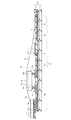
図2は、図1に示すA−B面で表示部21と電極端子部22とを切断したときの断面図である。なお、この図2には、出力側の配線3a−2,測定配線4−2,電極端子5a−2の構成は図示されないが、これらの構成は出力側の配線3a−1,測定配線4−1,電極端子5a−1の構成と同じである。そこで、以下の説明では、配線3a−1,3a−2をまとめて配線3aと記し、測定配線4−1,4−2をまとめて測定配線4と記し、電極端子5a−1,5a−2をまとめて電極端子5aと記すことにする。図2には、これまで説明してきたソース配線側の電極端子部22が示されている。図2に示すように、電極基板1の周縁部上にはゲート絶縁膜8が積層され、このゲート絶縁膜8上に出力側の配線3a、入力側の配線3b、および、測定配線4が形成されている。
2 is a cross-sectional view of the
図に示すように、ドライバーLSI6の裏面には、複数のバンプ6a,6bが設けられている。出力側の配線3aの表示部21と反対側の先端部には、ドライバーLSI6の出力バンプ6aを接合するための電極端子5aが接して設けられる。さらに、中間部には、出力側の配線3aから分岐された測定配線4が設けられている。そして、測定配線4上には、保護膜9が設けられ、さらに、分岐点を除く測定配線4真上に位置する保護膜9上に、ITOからなる導電性パターン部7が設けられている。こうして、導電性パターン部7は、分岐点を除く測定配線4上に第1の絶縁層である保護膜9を介して形成されている。
As shown in the drawing, a plurality of
一方、入力側の配線3bの表示部21側の先端部には、ドライバーLSI6の入力バンプ6bを接合するための電極端子5bが接して設けられ、他方の先端部には外部入力の電極端子5cが接して設けられている。上述の電極端子5a,5bは、ドライバーLSI6のバンプ6a,6bと同数である必要があり、これら電極端子5a,5bは近接して配置されることで電極端子ブロックを構成している。
On the other hand, an
次に、本実施の形態に係る液晶表示装置を形成する製造方法について説明する。最初に、電極基板1を形成する製造方法と、電極基板1に電極端子部22を形成する製造方法とについて説明する。まず、例えば、無アルカリガラスからなる透明絶縁性基板上に、スパッタリングにより、例えば、Cr,Al,Ta,Ti,Moからなる金属膜、あるいは、当該金属成分を主成分とする合金膜を成膜する。その後、写真製版技術によりパターニングすることで、表示部21のゲート電極、表示部21のゲート配線、電極端子部のゲート配線を同時に形成する。
Next, a manufacturing method for forming the liquid crystal display device according to the present embodiment will be described. First, a manufacturing method for forming the
次に、プラズマCVDを用いて、例えば、SiNをさらに成膜し、ゲート絶縁膜8を形成する。続いて、ゲート電極およびゲート配線、ゲート絶縁膜8上に、チャネル層となるアモルファスSiおよびコンタクト層となるN+型のアモルファスSiを連続して形成する。成膜後に、写真製版技術によりパターニングして表示部21の各液晶表示素子を駆動するための薄膜トランジスタを形成する。さらに、スパッタリングにて、例えば、Cr,Al,Moからなる金属膜、あるいは、当該金属成分を主成分とする合金膜を成膜する。その後、写真製版技術によりパターニングを行うことで、表示部21のドレイン電極およびソース電極、表示部21のソース配線、電極端子部22のソース配線3a,3bを同時に形成する。
Next, for example, SiN is further formed by plasma CVD, and the gate insulating film 8 is formed. Subsequently, amorphous Si serving as a channel layer and N + type amorphous Si serving as a contact layer are successively formed on the gate electrode, the gate wiring, and the gate insulating film 8. After film formation, patterning is performed by photolithography to form a thin film transistor for driving each liquid crystal display element of the
次に、表示部21の液晶層にDC成分が印加されるのを防ぐために、プラズマCVDにより、例えば、SiNからなる膜を成膜し、保護膜9を形成する。その後、ゲート配線の電極端子、および、ソース配線3a,3bの電極端子5a,5b,5cが形成される部分の保護膜9を除去する。本製造方法の最後の工程として、スパッタリングにてITO膜を成膜し、写真製版技術によりパターニングして、表示部21の画素電極と同時に、導電性パターン部7を形成する。これにより、導電性パターン部7は、表示部21の液晶表示素子の導電膜である画素電極と同一の工程で形成される。また、これら導電性パターン部7、表示部21の液晶表示素子の形成と同時に、ゲート配線の電極端子、および、ソース配線3a,3bの電極端子5a,5b,5cを形成する。
Next, in order to prevent the DC component from being applied to the liquid crystal layer of the
ITOを上から成膜することによって、Cr,Al等の材料で形成された配線部分が露出せず、電極端子に酸化膜が形成されるのを防止でき、その結果、その配線部分の導通不良の発生を防ぐことができる。以上の工程を経て、本実施の形態に係る液晶表示装置の電極基板1、および、電極端子部22が形成される。なお、対向基板2の製造方法や、電極基板1と対向基板2とを重ね合わせて接着し、液晶を注入する組立工程については、ここでは説明を省略する。
By forming the ITO film from above, it is possible to prevent the wiring part formed of a material such as Cr or Al from being exposed and prevent the oxide film from being formed on the electrode terminal. Can be prevented. Through the above steps, the
次に、ドライバーLSI6を電極端子部22に搭載する方法を図3に基づいて説明する。電極基板1の周縁上に形成された電極端子5a,5b上に、ACF(Anisotropic Conductive Film)10を貼り付ける。図3では、ACF10と後述するコート材12との境界は、破線で示されている。次に、ドライバーLSI6の裏面に形成された、例えば、Auからなる複数のバンプ6a,6bと、電極端子5a,5bとを精度よくアライメントした後、加熱加圧ツールを用いて熱圧着する。このときの条件は、例えば、加熱温度170〜200℃、処理時間10〜20秒、圧力30〜100Paにする。
Next, a method of mounting the
ACF10は、絶縁性のエポキシ樹脂に導電粒子10aを混ぜ合わせたものである。このACF10は、熱圧着があった箇所で、かつ、その方向に対してのみ、内部の導電粒子10aにより導電経路を形成するが、その他の箇所、その他の方向に対しては、内部のエポキシ樹脂により絶縁性が保たれる。そのため、上述のように熱圧着することにより、ドライバーLSI6の出力バンプ6aと電極端子5aとの間、および、入力バンプ6bと電極端子5bとの間それぞれに挟まったACF10の導電粒子10aが、バンプ6a,6bと電極端子5a,5bとを導通させる。すなわち、ACF10を介して熱圧着することで、ドライバーLSI6が、電極端子5a,5bと電気的に接続される。その一方で、ACF10の導通方向に対する水平方向は、ACF10内の絶縁性のエポキシ樹脂により絶縁性が保たれる。
The
続いて、外部から入力するためのFPC(Flexible Printed Circuit)11と、外部入力用の電極端子5cとの接続も同様にACF10を用いて行う。なお、FPC11は、例えば、厚さ30〜70μm程度のポリイミドフィルム、厚さ8〜25μmの銅箔11a、および、ポリイミド系のソルダーレジストにより構成する。
Subsequently, the
本搭載方法の最後の工程として、ドライバーLSI6とFPC11との間の配線3bを含む電極端子部22に、絶縁性のコート材12を塗布する。コート材12としては、主にシリコン樹脂、アクリル樹脂、フッ素樹脂、ウレタン樹脂等が用いられ、ディスペンサーを用いて塗布される。このコート材12を、電極端子部22に塗布することにより、配線3a,3b、測定配線4の腐食を防止することができる。
As the last step of the mounting method, the insulating
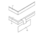
次に、図4を用いて、液晶表示装置の組立方法を説明する。本実施の形態に係る液晶表示装置は、上述の工程によりドライバーLSI6を電極基板1に搭載済みの液晶パネル16を、平面発光源となるバックライト18に載せ、液晶パネル16の前面側よりフロントフレーム17を嵌め込むことで組立てる。また、電極基板1に接続されたFPC11は、回路基板15と接続させる。
Next, a method for assembling the liquid crystal display device will be described with reference to FIG. In the liquid crystal display device according to the present embodiment, the
次に、本実施の形態に係る液晶表示装置において、表示不良が発生した際の検査方法を図5、および、図6を用いて説明する。なお、図6は、図5の平面図をC−Dで切断した場合の断面図である。ここでは、仮に、図5の右から1番目の配線3a−1に不良が発生していると仮定して説明する。検査方法の最初の工程として、表示部21において不良が発生した配線3aを特定し、当該特定した一の配線3a−1からの測定配線4−1と、当該測定配線4−1上の導電性パターン部7とをレーザー照射によって接続する。
Next, an inspection method when a display defect occurs in the liquid crystal display device according to the present embodiment will be described with reference to FIGS. 6 is a cross-sectional view of the plan view of FIG. 5 taken along the line CD. Here, it is assumed that a defect has occurred in the
本実施の形態では、ドライバーLSI6、および、FPC11を搭載した後の液晶表示パネルにおいて、信号発生器から各ソース配線3aに順次信号を入力する。信号の入力により、表示部21において所定の映像信号が得られなかった箇所、すなわち、線欠陥等の表示不良が発生した配線3aのアドレスを、信号発生器の機能により特定する。ここでは、図5に示した配線3a−1に不良が発生していると仮定しているため、信号発生器により配線3a−1が特定される。
In this embodiment, in the liquid crystal display panel after mounting the
次に、当該アドレスの配線3a−1の測定パターン部(測定配線4−1の先端)と、導電性パターン部7との重ね合わせ部に対し、電極基板1の裏面側、すなわち、ガラス基板側からレーザーを照射する。図5では、右から1番目の配線3a−1の測定配線4−1の先端にレーザーを照射して、レーザー痕14aが形成された状態が示されている。レーザー痕14aが形成された箇所では、レーザー照射で発生する熱により、測定配線4−1の先端の金属が保護膜9を突き破って導電性パターン部7と接触している。その結果、測定配線4−1の先端と導電性パターン部7とが短絡し電気的に接続する。図6の断面図では、測定配線4−1と導電性パターン部7とが短絡している様子が示されている。なお、確実な導通をとるためには、レーザーの照射を数回に分けて行うことが望ましい。
Next, the back surface side of the
上述のレーザー照射により測定配線4−1の先端と導電性パターン部7とを導通させた後に、当該導電性パターン部7に、測定器、例えば、オシロスコープまたはディジタルマルチメータのプローブまたは針を接触させる。こうして、測定配線4−1と接続された導電性パターン部7に、測定器を接続させることによって、ドライバーLSI6からの出力を測定し、不良原因を究明する。ここでいうドライバーLSI6からの出力は、例えば、出力信号または出力波形が該当する。このように、一の導電性パターン部7は、配線3a−1,3a−2に共有されているものの、不良が発生した一の配線3a−1を導電性パターン部7に個別に電気的に接続する。そのため、同一のドライバーLSI6に接続された複数の配線3aの不良原因の究明を配線ごとに行うことができる。
After conducting the conduction between the tip of the measurement wiring 4-1 and the
以上は、一の導電性パターン部7を共有している配線3a−1,3a−2片方に不良が発生した場合について説明した。次に、図7を用いて、一の導電性パターン部7を共有している配線3a−1,3a−2両方に不良が発生し、上述の信号発生器により配線3a−1,3a−2両方が特定された場合について説明する。なお、配線3a−1の不良原因を究明する方法については、上述と同様であるため省略する。
The case where a defect has occurred in one of the
配線3a−1の不良原因を究明した後、上述のレーザー照射で接続した一の配線3a−1からの測定配線4−1を、配線3a−1と導電性パターン部7の間において、レーザー照射によって切断する。本実施の形態では、測定配線4−1の分岐点近傍にレーザー照射することによって測定配線4−1を切断する。このレーザー照射後には、その分岐点近傍にレーザー痕14bが形成される。信号発生器により特定した他の配線3a−2からの測定配線4−2と、当該測定配線4−2上の導電性パターン部7とをレーザー照射によって接続する。
After investigating the cause of the defect of the
本実施の形態では、配線3a−2の測定配線4−2の先端と、導電性パターン部7との間にレーザーを照射することによって、測定配線4−2と導電性パターン部7とを導通させる。レーザー照射後には、レーザー痕14cが形成される。このレーザー照射により測定配線4−2と接続された導電性パターン部7に、上述と同様、測定器のプローブまたは針を接触させることによって、測定器によりドライバーLSI6からの出力を測定し、不良原因を究明する。
In the present embodiment, the measurement wiring 4-2 and the
以上のような本実施の形態に係る液晶表示装置によれば、導電性パターン部7は、電極基板1の周縁部に位置する測定配線4上に、絶縁層である保護膜9を介して形成される。そのため、故障解析時にレーザー照射により、解析の対象となる配線3aと導電パターン部7とを接続することによって、容易にドライバーLSI6の出力、例えば、出力信号または出力波形を検査することができる。また、配線3a−1,3a−2が一の導電性パターン部7を共有するため、導電性パターン部7の数を削減することができる。これにより、導電性パターン部7を小さくすることなく、配線3a−1,3a−2間のピッチを狭くすることができ、その結果、バンプ間のピッチを狭くすることができる。こうして、将来のドライバーLSI6の多出力化に対応することができる。また、導電性パターン部7の下に、測定配線4が形成されているので、レーザーを電極基板1の裏面側から照射する際に、照射箇所を特定しやすく作業効率が向上する。また、導電性パターン部7は、分岐点を除いた測定配線4上に形成されるため、2回目の配線の検査時において、分岐点にレーザー照射することにより、測定配線4の切断を容易にすることができる。
According to the liquid crystal display device according to the present embodiment as described above, the
また、本実施の形態に係る液晶表示装置では、導電性パターン部7が千鳥上に配置されている。そのため、導電性パターン部7を小さくすることなく、配線3a−1,3a−2間のピッチを狭くすることができ、その結果、バンプ間のピッチをさらに狭くすることができる。
Moreover, in the liquid crystal display device according to the present embodiment, the
また、本実施の形態に係る液晶表示装置では、導電性パターン部7は、表示部21の画素電極と同一の工程で形成される。これにより、製造工程を簡略化させ、コストを低減することができる。
In the liquid crystal display device according to the present embodiment, the
また、本実施の形態に係る液晶表示装置の検査方法では、一の導電性パターン部7が配線3a−1,3a−2に共有されているものの、導電性パターン部7と、不良が発生した一の配線3a−1とを個別に電気的に接続する。これにより、一のドライバーLSI6に接続された複数の配線3aに係る不良原因の究明を個別に行うことができる。なお、本実施の形態では、レーザー照射により先に接続される一の配線を配線3a−1であるものとして説明したが、一の配線が配線3a−2であっても、同様の効果を得ることができる。
Further, in the inspection method for the liquid crystal display device according to the present embodiment, although one
また、本実施の形態に係る液晶表示装置の検査方法によれば、導電性パターン部7と接続した一の配線3a−1をレーザー照射により切断した後に、導電性パターン部7と他の配線3a−2とをレーザー照射により接続する。これにより、先に検査した一の配線3a−1と独立して、他の配線3a−2に係る不良原因の究明を個別に行うことができる。
Further, according to the inspection method of the liquid crystal display device according to the present embodiment, after cutting one
ここまでは、本実施の形態に係る液晶表示装置の主要な構成およびその検査方法の主要な工程を説明した。次に、より望ましい液晶表示装置を、図8から図11を用いて説明する。図8に係る液晶表示装置では、一の配線3a−1から複数の測定配線4−1A,4−1Bが分岐して設けられ、一の導電性パターン部7は、一の配線3a−1からの複数の測定配線4−1A,4−1B同士にまたがって形成される。同様に、一の配線3a−2から複数の測定配線4−2A,4−2Bが分岐して設けられ、一の導電性パターン部7は、一の配線3a−2からの複数の測定配線4−2A,4−2B同士にまたがって形成される。
Up to this point, the main configuration of the liquid crystal display device according to the present embodiment and the main steps of the inspection method have been described. Next, a more desirable liquid crystal display device will be described with reference to FIGS. In the liquid crystal display device according to FIG. 8, a plurality of measurement wires 4-1A and 4-1B are branched from one
このように形成された液晶表示装置によれば、複数の測定配線4−1A,4−1Bの複数個所において、配線3a−1と導電性パターン部7とを接続することができる。こうして、複数個所で接続することにより、接続抵抗を下げることができるため、よりよい条件でドライバーLSI6からの出力信号または出力波形を測定し、不良原因を究明することができる。
According to the liquid crystal display device thus formed, the
図9および図10に係る液晶表示装置では、各複数の配線3a−1,3a−2は、保護膜9を介して、対応する導電性パターン部7の下に配置されている。ここで、対応する導電性パターン部7とは、各配線3aから分岐してなる各測定配線4上に設けられた導電性パターン部7をいう。これにより、図1および図8に係る液晶表示装置よりもさらに配線3a−1,3a−2間のピッチをさらに狭くすることができる。
In the liquid crystal display device according to FIGS. 9 and 10, each of the plurality of
図11に係る液晶表示装置では、一の配線3a−2から分岐した測定配線4−2A,4−2Bと、測定配線4−2Cは、互いに異なる導電性パターン部7A,7Bの下に設けられている。これにより、導電性パターン部7A,7Bのいずれにおいても、配線3a−2に係る不良原因の究明を行うことができる。こうして、導電性パターン部7A,7Bの数を増やさなくても、ドライバーLSI6からの配線3a−2に係る出力信号または出力波形を測定できる箇所を増やすことができ、それらを比較することが容易となる。
In the liquid crystal display device according to FIG. 11, the measurement wires 4-2A and 4-2B branched from the one
<実施の形態2>
実施の形態1では、電極基板1の周縁部に形成される電極端子部22は、ソース配線側の電極端子部であるもとして説明した。本実施の形態では、電極基板1の周縁部に形成される電極端子部22は、ゲート配線側の電極端子部であるものとして説明する。図12は、本実施の形態に係る液晶表示装置の表示部21と電極端子部22とを切断したときの断面図である。なお、実施の形態1に係る液晶表示装置の構成に対応する本実施の形態に係る液晶表示装置の構成には、同一符号を付すものとする。
<
In
本実施の形態に係る液晶表示装置では、実施の形態1に係る液晶表示装置と同様、複数の配線3aは、電極基板1に形成され、表示部21の複数の液晶表示素子に信号を供給する。出力側の配線3aの表示部21と反対側の先端部には、ドライバーLSI6の出力バンプ6aが接合される電極端子5aが接して設けられている。入力側の配線3bの表示部21側の先端部には、ドライバーLSI6の入力バンプ6bが接合される電極端子5bが接して設けられている。電極端子5a,5bは、ドライバーLSI6の複数のバンプ6a,6bと同数必要であり、これら電極端子5a,5bは近接して配置されることで、電極端子ブロックを構成している。また、測定配線4は、表示部21とドライバーLSI6との間に位置する各複数の配線3aの配線を分岐してなる。本実施の形態では、測定配線4は、配線3aの中間部から分岐してなる。
In the liquid crystal display device according to the present embodiment, as in the liquid crystal display device according to the first embodiment, the plurality of
本実施の形態に係るゲート配線側の電極端子部22は、実施の形態1に係る電極端子部と異なり、配線3a,3b、および、測定配線4は、ゲート絶縁膜8下に形成される。測定配線4上には、ゲート絶縁膜8を介してメタルパット部13が設けられている。このメタルパット部13の上部には、保護膜9を介してITOの導電性パターン部7が設けられている。
Unlike the electrode terminal part according to the first embodiment, the
こうして、本実施の形態に係る導電性パターン部7は、分岐点を除く測定配線4上に第1の絶縁層であるゲート絶縁膜8を介して形成され、各複数の配線3aから分岐した測定配線4同士にまたがって形成される。そして、本実施の形態に係る液晶表示装置は、ゲート絶縁膜8と導電性パターン部7との間に、メタルパット部13と、第2の絶縁膜である保護膜9とを備える。メタルパット部13は、測定配線4上側に設けられ、ゲート絶縁膜8上に設けられる。保護膜9は、メタルパット部13上に設けられる。つまり、実施の形態1では、測定配線4−保護膜9−導電性パターン部7を順に積層した構成であったのに対し、本実施の形態では、測定配線4−ゲート絶縁膜8−メタルパット部13−保護膜9−導電性パターン部7を順に積層した構成である。
Thus, the
本実施の形態において、電極基板1を形成する製造方法、電極基板1に電極端子部22を形成する製造方法、ドライバーLSI6を電極端子部22に搭載する方法、液晶表示装置の組立方法は、実施の形態1と同じであるため、詳細な説明は省略する。次に、本実施の形態に係る液晶表示装置において表示不良が発生した場合の検査方法について説明する。基本的には、本実施の形態に係る検査方法は、実施の形態1に係る検査方法とほぼ同じである。
In the present embodiment, a manufacturing method for forming the
検査方法の最初の工程として、ドライバーLSI6、および、FPC11を搭載した後の液晶表示パネルにおいて、信号発生器から各ゲート配線3aに順次信号を入力する。信号の入力により、表示部21において所定の映像信号が得られなかった箇所、すなわち、線欠陥等の表示不良が発生した配線3aのアドレスを、信号発生器の機能により特定する。次に、当該アドレスの配線3aの測定配線4の先端と、導電性パターン部7との重ね合わせ部に対し、電極基板1の裏面側、すなわち、ガラス基板側からレーザーを照射する。そうすると、レーザー痕14aが形成される。
As the first step of the inspection method, signals are sequentially input from the signal generator to each
レーザー痕14aが形成された箇所では、レーザー照射で発生する熱により、測定配線4の先端の金属がゲート絶縁膜8を突き破ってメタルパット部13と接触する。さらに、メタルパット部13の金属が保護膜9を突き破って導電性パターン部7と接触している。これにより、測定配線4と導電性パターン部7とが短絡し電気的に接続している。なお、確実な導通をとるためには、レーザーの照射を数回に分けて行うことが望ましい。
At the place where the
上述のレーザー照射により測定配線4の先端と導電性パターン部7とを導通させた後に、当該導電性パターン部7に、測定器、例えば、オシロスコープまたはディジタルマルチメータのプローブまたは針を接触させる。こうして、測定配線4と接続された導電性パターン部7に、測定器を接続させることによって、ドライバーLSI6からの出力を測定し、不良原因を究明する。
After the tip of the
以上の構成からなる本実施の形態に係る液晶表示装置によれば、また、メタルパット部13を設けることにより、レーザーにより絶縁層である保護膜9を突き破る金属が多くなるため、測定配線4と導電性パターン部7との導通の確保を容易にすることができる。
According to the liquid crystal display device according to the present embodiment having the above-described configuration, since the
なお、本実施の形態においても、図8〜11に示すような測定配線4と導電性パターン部7を設けてもよい。このように構成すれば、実施の形態1で説明した効果を同様に得ることができる。例えば、図8に示すような測定配線4と導電性パターン部7を設けた場合には、実施の形態1と同様、複数の測定配線4−1A,4−1Bと導電性パターン部7とを接続して、接続抵抗を下げることができる。そのため、よりよい条件でドライバーLSI6からの出力信号または出力波形を測定し、不良原因を究明することができる。
Also in this embodiment, the
1 電極基板、2 対向基板、3a,3a−1,3a−2,3b 配線、4,4−1,4−1A,4−1B,4−1C,4−2,4−2A,4−2B,4−2C 測定配線、5a,5a−1,5a−2,5b,5c 電極端子、6 ドライバーLSI、7,7A,7B 導電性パターン部、8 ゲート絶縁膜、9 保護膜、10 ACF、11 FPC、12 コート材、13 メタルパット部、14a〜c レーザー痕、15 回路基板、16 液晶パネル、17 フロントフレーム、18 バックライト、21 表示部、22 電極端子部。 1 electrode substrate, 2 counter substrate, 3a, 3a-1, 3a-2, 3b wiring, 4,4-1, 4-1A, 4-1B, 4-1C, 4-2, 4-2A, 4-2B , 4-2C measurement wiring, 5a, 5a-1, 5a-2, 5b, 5c electrode terminal, 6 driver LSI, 7, 7A, 7B conductive pattern portion, 8 gate insulating film, 9 protective film, 10 ACF, 11 FPC, 12 coating material, 13 metal pad part, 14a-c laser mark, 15 circuit board, 16 liquid crystal panel, 17 front frame, 18 backlight, 21 display part, 22 electrode terminal part.
Claims (11)
前記絶縁性基板の少なくとも一方に形成され、前記複数の表示素子に信号を供給する複数の配線と、
前記絶縁性基板の周縁部に設けられ、前記複数の配線の端子と接続することで前記複数の表示素子を駆動するドライバーLSIと、
前記表示部と前記ドライバーLSIとの間に位置する各前記複数の配線を分岐してなる測定配線と、
分岐点を除く前記測定配線上に第1の絶縁層を介して形成され、各前記複数の配線から分岐した前記測定配線同士にまたがって形成される導電性パターン部とを備える、
液晶表示装置。 A liquid crystal layer sandwiched between two insulating substrates facing each other, and a display unit in which a plurality of display elements are formed;
A plurality of wirings formed on at least one of the insulating substrates and supplying signals to the plurality of display elements;
A driver LSI that is provided at a peripheral portion of the insulating substrate and drives the plurality of display elements by connecting to terminals of the plurality of wirings;
A measurement wiring formed by branching each of the plurality of wirings located between the display unit and the driver LSI;
A conductive pattern formed on the measurement wiring excluding the branch point via the first insulating layer and formed across the measurement wirings branched from the plurality of wirings;
Liquid crystal display device.
前記導電性パターン部は、前記偶数アドレスの配線から分岐した前記測定配線と、前記奇数アドレスの配線から分岐した前記測定配線とにまたがって形成される、
請求項1に記載の液晶表示装置。 The plurality of wirings include an even address (2n) wiring and an odd address (2n + 1) wiring,
The conductive pattern portion is formed across the measurement wiring branched from the even address wiring and the measurement wiring branched from the odd address wiring.
The liquid crystal display device according to claim 1.
請求項1または請求項2に記載の液晶表示装置。 The conductive pattern portions are arranged in a staggered manner,
The liquid crystal display device according to claim 1.
一の前記導電性パターン部は、前記一の配線からの前記複数の測定配線同士にまたがって形成される、
請求項1乃至請求項3のいずれかに記載の液晶表示装置。 A plurality of the measurement wires are branched from the one wire,
The one conductive pattern portion is formed across the plurality of measurement wirings from the one wiring.
The liquid crystal display device according to claim 1.
前記第1の絶縁層を介して、対応する前記導電性パターン部の下に配置されている、
請求項1乃至請求項4のいずれかに記載の液晶表示装置。 Each of the plurality of wires is
Disposed under the corresponding conductive pattern portion via the first insulating layer,
The liquid crystal display device according to claim 1.
請求項5に記載の液晶表示装置。 At least two of the measurement wires branched from the one wire are provided under the different conductive pattern portions,
The liquid crystal display device according to claim 5.
前記測定配線上側に設けられ、前記第1の絶縁層上に設けられたメタルパット部と、
前記メタルパット部上に設けられた第2の絶縁層とをさらに備える、
請求項1乃至請求項6のいずれかに記載の液晶表示装置。 Between the first insulating layer and the conductive pattern portion,
A metal pad portion provided on the measurement wiring and provided on the first insulating layer;
A second insulating layer provided on the metal pad portion;
The liquid crystal display device according to claim 1.
請求項1乃至請求項7のいずれかに記載の液晶表示装置。 The conductive pattern portion is covered with a coating material,
The liquid crystal display device according to claim 1.
請求項1乃至請求項8のいずれかに記載の液晶表示装置。 The conductive pattern portion is formed in the same process as the conductive film of the display element of the display portion.
The liquid crystal display device according to claim 1.
(a)前記表示部において不良が発生した前記配線を特定し、当該特定した一の前記配線からの前記測定配線と、当該測定配線上の前記導電性パターン部とをレーザー照射によって接続する工程と、
(b)前記工程(a)により前記測定配線と接続された前記導電性パターン部に、測定器を接続させることによって、前記ドライバーLSIからの出力を測定する工程とを備える、
液晶表示装置の検査方法。 A method for inspecting a liquid crystal display device according to any one of claims 1 to 9,
(A) identifying the wiring in which a defect has occurred in the display unit, and connecting the measurement wiring from the identified one wiring and the conductive pattern portion on the measurement wiring by laser irradiation; ,
(B) comprising a step of measuring an output from the driver LSI by connecting a measuring instrument to the conductive pattern portion connected to the measurement wiring in the step (a).
Inspection method for liquid crystal display devices.
(d)前記工程(a)で特定した他の前記配線からの前記測定配線と、当該測定配線上の前記導電性パターン部とをレーザー照射によって接続する工程と、
(e)前記工程(d)により前記測定配線と接続された前記導電性パターン部に、測定器を接続させることによって、前記ドライバーLSIからの出力を測定する工程とをさらに備える、
請求項10に記載の液晶表示装置の検査方法。 (C) after the step (b), cutting the measurement wiring from the one wiring connected in the step (a) by laser irradiation;
(D) connecting the measurement wiring from the other wiring specified in the step (a) and the conductive pattern portion on the measurement wiring by laser irradiation;
(E) further comprising a step of measuring an output from the driver LSI by connecting a measuring instrument to the conductive pattern portion connected to the measurement wiring in the step (d).
The method for inspecting a liquid crystal display device according to claim 10.
Priority Applications (2)
| Application Number | Priority Date | Filing Date | Title |
|---|---|---|---|
| JP2008030100A JP2009192572A (en) | 2008-02-12 | 2008-02-12 | Liquid crystal display device and inspection method thereof |
| US12/366,984 US20090201456A1 (en) | 2008-02-12 | 2009-02-06 | Liquid crystal display device and inspection method thereof |
Applications Claiming Priority (1)
| Application Number | Priority Date | Filing Date | Title |
|---|---|---|---|
| JP2008030100A JP2009192572A (en) | 2008-02-12 | 2008-02-12 | Liquid crystal display device and inspection method thereof |
Publications (1)
| Publication Number | Publication Date |
|---|---|
| JP2009192572A true JP2009192572A (en) | 2009-08-27 |
Family
ID=40938586
Family Applications (1)
| Application Number | Title | Priority Date | Filing Date |
|---|---|---|---|
| JP2008030100A Pending JP2009192572A (en) | 2008-02-12 | 2008-02-12 | Liquid crystal display device and inspection method thereof |
Country Status (2)
| Country | Link |
|---|---|
| US (1) | US20090201456A1 (en) |
| JP (1) | JP2009192572A (en) |
Cited By (1)
| Publication number | Priority date | Publication date | Assignee | Title |
|---|---|---|---|---|
| WO2018101159A1 (en) * | 2016-12-01 | 2018-06-07 | シャープ株式会社 | Connection wiring |
Families Citing this family (3)
| Publication number | Priority date | Publication date | Assignee | Title |
|---|---|---|---|---|
| CN102023271B (en) * | 2010-11-25 | 2012-11-28 | 河南省电力公司洛阳供电公司 | Spare power automatic switching logic test method for verifying automatic switching modes of high voltage side buscouple switch |
| CN102095951B (en) * | 2010-11-25 | 2013-03-13 | 河南省电力公司洛阳供电公司 | Spare power automatic switching logic test method for checking automatic switching mode of low-pressure side section switch |
| CN102072997B (en) * | 2010-11-25 | 2014-09-10 | 河南省电力公司洛阳供电公司 | Spare automatic switching logic test method for checking main transformer mutual switching mode |
Family Cites Families (3)
| Publication number | Priority date | Publication date | Assignee | Title |
|---|---|---|---|---|
| US5076666A (en) * | 1988-12-06 | 1991-12-31 | Sharp Kabushiki Kaisha | Active matrix display apparatus with drain electrode extensions |
| JP3943919B2 (en) * | 2001-12-04 | 2007-07-11 | 株式会社アドバンスト・ディスプレイ | Liquid crystal display device and inspection method thereof |
| JP4202300B2 (en) * | 2004-06-24 | 2008-12-24 | 三菱電機株式会社 | Liquid crystal display device and method for inspecting liquid crystal display device |
-
2008
- 2008-02-12 JP JP2008030100A patent/JP2009192572A/en active Pending
-
2009
- 2009-02-06 US US12/366,984 patent/US20090201456A1/en not_active Abandoned
Cited By (1)
| Publication number | Priority date | Publication date | Assignee | Title |
|---|---|---|---|---|
| WO2018101159A1 (en) * | 2016-12-01 | 2018-06-07 | シャープ株式会社 | Connection wiring |
Also Published As
| Publication number | Publication date |
|---|---|
| US20090201456A1 (en) | 2009-08-13 |
Similar Documents
| Publication | Publication Date | Title |
|---|---|---|
| JP3943919B2 (en) | Liquid crystal display device and inspection method thereof | |
| CN100381890C (en) | Liquid crystal display device and inspection method of liquid crystal display device | |
| KR101579853B1 (en) | Display panel | |
| KR101571768B1 (en) | DISPLAY SUBSTRATE, MISUSE REPAIR METHOD OF THE SAME, AND MOTHER PLATE WITH THE DISPLAY SUBSTRATE | |
| CN104238154B (en) | The manufacture method of liquid crystal display device and liquid crystal display device | |
| JP2009282285A (en) | Image display device and mounting inspection method thereof | |
| US8354672B2 (en) | Thin film transistor array panel | |
| JP2006098455A (en) | Mounting structure, mounting substrate, electro-optical device, and electronic apparatus | |
| JP2009192572A (en) | Liquid crystal display device and inspection method thereof | |
| KR20080099411A (en) | Test pad, manufacturing method thereof, liquid crystal display device having same and manufacturing method thereof | |
| JP4177222B2 (en) | Liquid crystal display device and inspection method thereof | |
| KR101682363B1 (en) | Flat panel display device and manufacturing method the same | |
| JP2011008051A (en) | Liquid crystal display device and inspection method for liquid crystal display device | |
| JP2006072032A (en) | Display device and inspection method of display device | |
| JP2003158354A (en) | Wiring board mounting inspection method | |
| CN114578594B (en) | Array substrate, display module thereof and manufacturing method | |
| JP2007226001A (en) | Electrooptical device | |
| KR100816335B1 (en) | Thin film transistor substrate and method for attaching driving integrated circuit using same | |
| JP2019176084A (en) | Board unit and display device | |
| JP5203485B2 (en) | Display device and displacement inspection method | |
| JP4938377B2 (en) | Inspection method for liquid crystal display devices | |
| TWI240104B (en) | Display assembly and assembling method thereof | |
| JP2008233423A (en) | Flat panel display device and wiring structure for inspection | |
| JP2010097860A (en) | Inspection apparatus of plasma display panel, connection device, and manufacturing method of plasma display device | |
| JP2007148209A (en) | Image display device and observation method of display drive waveform thereof |