JP2009192594A - Plasma display device - Google Patents
Plasma display device Download PDFInfo
- Publication number
- JP2009192594A JP2009192594A JP2008030280A JP2008030280A JP2009192594A JP 2009192594 A JP2009192594 A JP 2009192594A JP 2008030280 A JP2008030280 A JP 2008030280A JP 2008030280 A JP2008030280 A JP 2008030280A JP 2009192594 A JP2009192594 A JP 2009192594A
- Authority
- JP
- Japan
- Prior art keywords
- period
- discharge
- cell initialization
- plasma display
- initialization pulse
- Prior art date
- Legal status (The legal status is an assumption and is not a legal conclusion. Google has not performed a legal analysis and makes no representation as to the accuracy of the status listed.)
- Withdrawn
Links
Images




Landscapes
- Control Of Indicators Other Than Cathode Ray Tubes (AREA)
- Control Of Gas Discharge Display Tubes (AREA)
Abstract
【課題】プラズマディスプレイ装置において、長期間黒を表示した場合においても、映像信号入力時に誤放電を発生させず表示品質の悪化を防ぐことを目的とする。
【解決手段】プラズマディスプレイ装置であって、1フィールドのうち全てのサブフィールドにおける点灯率が特定の閾値以下となる無映像期間は、全セル初期化パルスの印加を停止するとともに、1フィールドのうち少なくとも1つのサブフィールドにおける前記点灯率が前記閾値を超える映像期間は、電圧が緩やかに上昇する期間の平均の電圧変化率が異なる2種類以上の全セル初期化パルスを印加するように構成し、かつ前記平均の電圧変化率が大きい全セル初期化パルスを印加する期間に先立って、平均の電圧変化率が小さい全セル初期化パルスを印加する期間を配置するように構成した。
【選択図】図4An object of the present invention is to prevent display quality from deteriorating without causing erroneous discharge when a video signal is input even in a case where black is displayed for a long time in a plasma display device.
In a plasma display device, during a non-video period in which lighting rates in all subfields of one field are below a specific threshold, application of all-cell initialization pulses is stopped and The video period in which the lighting rate in at least one subfield exceeds the threshold is configured to apply two or more types of all-cell initialization pulses having different average voltage change rates during a period in which the voltage gradually increases. In addition, a period for applying the all-cell initialization pulse having a small average voltage change rate is arranged prior to the period for applying the all-cell initialization pulse having a large average voltage change rate.
[Selection] Figure 4
Description
本発明は、プラズマディスプレイパネル(以下、パネルという)を表示デバイスとして用いたプラズマディスプレイ装置に関するものである。 The present invention relates to a plasma display apparatus using a plasma display panel (hereinafter referred to as a panel) as a display device.
このプラズマディスプレイ装置に用いられるパネルは、大別して、駆動的にはAC型とDC型があり、放電形式では面放電型と対向放電型の2種類があるが、高精細化、大画面化および製造の簡便性から、現状では、プラズマディスプレイ装置の主流は、3電極構造の面放電型のものである。 Panels used in this plasma display device are roughly classified into AC type and DC type in terms of driving, and there are two types of discharge types: surface discharge type and counter discharge type. Due to the simplicity of manufacturing, at present, the mainstream of plasma display devices is a surface discharge type having a three-electrode structure.
この面放電型のプラズマディスプレイパネル構造は、少なくとも前面側が透明な一対の基板を基板間に放電空間が形成されるように対向配置するとともに、前記放電空間を複数に仕切るための隔壁を基板に配置し、かつ前記隔壁により仕切られた放電空間で放電が発生するように基板に電極群を配置するとともに放電により発光する赤色、緑色、青色に発光する蛍光体を設けて複数の放電セルを構成したもので、放電により発生する波長の短い真空紫外光によって蛍光体を励起し、赤色、緑色、青色の放電セルからそれぞれ赤色、緑色、青色の可視光を発することによりカラー表示を行っている。 In this surface discharge type plasma display panel structure, at least a pair of substrates whose front sides are transparent are arranged to face each other so that a discharge space is formed between the substrates, and partition walls for dividing the discharge space into a plurality of substrates are arranged on the substrate. In addition, a plurality of discharge cells are configured by arranging an electrode group on the substrate so that a discharge is generated in the discharge space partitioned by the barrier ribs, and providing phosphors that emit red, green, and blue light emitted by the discharge. However, phosphors are excited by vacuum ultraviolet light having a short wavelength generated by discharge, and red, green, and blue visible light is emitted from red, green, and blue discharge cells, respectively, to perform color display.
このようなプラズマディスプレイ装置は、液晶パネルに比べて高速の表示が可能であり、視野角が広いこと、大型化が容易であること、自発光型であるため表示品質が高いことなどの理由から、フラットパネルディスプレイの中で最近特に注目を集めており、多くの人が集まる場所での表示装置や家庭で大画面の映像を楽しむための表示装置として各種の用途に使用されている。 Such a plasma display device can display at a higher speed than a liquid crystal panel, has a wide viewing angle, is easy to enlarge, and is self-luminous so that the display quality is high. Recently, the flat panel display has attracted particular attention and is used for various purposes as a display device in a place where many people gather and a display device for enjoying a large screen image at home.
このようなプラズマディスプレイ装置においては、パネルの駆動方法として、アドレス放電を生じやすい状態に壁電荷を調整する初期化期間と、入力映像信号に応じてアドレス放電を行うアドレス期間と、アドレス放電が生じた放電セルで維持放電を生じさせることによって表示発光を行う維持期間を含むサブフィールドという単位を1フィールド内で複数回繰り返すことによってプラズマディスプレイ装置の階調表示を行う方法が一般的に用いられる。 In such a plasma display device, as a panel driving method, an initialization period in which wall charges are adjusted in a state where address discharge is likely to occur, an address period in which address discharge is performed in accordance with an input video signal, and address discharge occur. In general, a method of performing gradation display of a plasma display device by repeating a unit called a subfield including a sustain period in which display light emission is performed by generating a sustain discharge in the discharge cells a plurality of times within one field is generally used.
このうち、初期化期間には、初期化パルスを印加して直前の状態に関係なく初期化放電を生じさせる全セル初期化期間と、直前に維持放電が生じたセルのみ初期化放電を生じさせる選択初期化期間の2種類があり、全セルに毎回必ず放電を生じさせて黒表示の輝度を上昇させる全セル初期化パルスを先頭のサブフィールドのみに設けることによって、1フィールドにおける初期化放電の回数を低減し、コントラストの向上を図る方法が用いられる(特許文献1参照)。
ところで、プラズマディスプレイ装置において、全ての放電セルが発光しない全画面黒表示の映像信号が入力された場合、全ての放電セルにおいてアドレス放電を生じさせる必要がないため、全セル初期化放電が必要なくなる。よって、全画面黒表示において全セル初期化パルスの印加を停止すれば黒輝度がほぼ0となって、高いコントラストが実現できる。 By the way, in the plasma display device, when an image signal of full screen black display in which all discharge cells do not emit light is input, it is not necessary to generate address discharge in all discharge cells, and therefore all cell initialization discharge is not necessary. . Therefore, if the application of the all-cell initialization pulse is stopped in the full screen black display, the black luminance becomes almost zero, and a high contrast can be realized.
しかし、このような駆動方法を用いた場合、全画面に黒を表示する期間に長く滞在した後に再び映像信号が入力されると、最初のフィールドにおける全セル初期化パルスで誤放電が発生して表示品質が悪化するという課題があった。 However, when such a driving method is used, if a video signal is input again after a long period of time during which black is displayed on the entire screen, an erroneous discharge occurs due to an all-cell initialization pulse in the first field. There was a problem that display quality deteriorated.
本発明はこのような現状に鑑みなされたもので、長期間黒を表示した場合においても、映像信号入力時に誤放電を発生させず表示品質の悪化を防ぐことを目的とする。 The present invention has been made in view of such a situation, and an object of the present invention is to prevent display quality from deteriorating without causing erroneous discharge when a video signal is input even when black is displayed for a long time.
この課題を解決するために本発明は、複数の表示電極を配置した前面基板と前記表示電極に交差するようにデータ電極を配置した背面基板とを間に放電空間が形成されるように対向配置して複数の放電セルを形成したプラズマディスプレイパネルを有し、電圧が緩やかに上昇する期間を有しかつ全ての放電セルで初期化放電を発生させる全セル初期化パルスを印加する初期化期間と、発光させる放電セルを選択するアドレス期間と、このアドレス期間で選択した放電セルで維持放電を行う維持期間とを設けて発光表示を行うプラズマディスプレイ装置であって、1フィールドのうち全てのサブフィールドにおける点灯率が特定の閾値以下となる無映像期間は、全セル初期化パルスの印加を停止するとともに、1フィールドのうち少なくとも1つのサブフィールドにおける前記点灯率が前記閾値を超える映像期間は、電圧が緩やかに上昇する期間の平均の電圧変化率が異なる2種類以上の全セル初期化パルスを印加するように構成し、かつ前記平均の電圧変化率が大きい全セル初期化パルスを印加する期間に先立って、平均の電圧変化率が小さい全セル初期化パルスを印加する期間を配置するように構成したことを特徴とする。 In order to solve this problem, the present invention is arranged so that a discharge space is formed between a front substrate on which a plurality of display electrodes are arranged and a rear substrate on which data electrodes are arranged so as to intersect the display electrodes. And a plasma display panel having a plurality of discharge cells, an initializing period in which a voltage gradually increases and an all-cell initializing pulse for generating initializing discharge in all the discharge cells is applied. A plasma display apparatus for performing light emission display by providing an address period for selecting a discharge cell to emit light and a sustain period for performing a sustain discharge in the discharge cell selected in the address period. During the non-video period in which the lighting rate at the time is equal to or less than a specific threshold, the application of the all-cell initialization pulse is stopped and at least one of the fields In the video period in which the lighting rate in the subfield exceeds the threshold value, two or more types of all-cell initialization pulses having different average voltage change rates during a period in which the voltage gradually rises are applied, and A period for applying an all-cell initialization pulse with a small average voltage change rate is arranged prior to a period for applying an all-cell initialization pulse with a high average voltage change rate.
本発明によれば、映像期間の開始時に電圧が緩やかに上昇する期間の平均の電圧変化率が小さい全セル初期化パルスを印加することによって、全セル初期化パルス印加時に発生する誤放電を防ぐことができるため、表示品質が悪化することなく高いコントラストを実現できるプラズマディスプレイ装置を得ることができる。 According to the present invention, by applying an all-cell initialization pulse having a small average voltage change rate during a period in which the voltage gradually rises at the start of the video period, erroneous discharge that occurs when the all-cell initialization pulse is applied is prevented. Therefore, it is possible to obtain a plasma display device that can realize high contrast without deteriorating display quality.
以下、本発明の実施の形態によるプラズマディスプレイ装置について、図1〜図10を用いて説明するが、本発明の実施の態様はこれに限定されるものではない。 Hereinafter, although the plasma display apparatus by embodiment of this invention is demonstrated using FIGS. 1-10, the aspect of this invention is not limited to this.
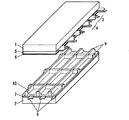
まず、プラズマディスプレイ装置におけるパネルの構造について図1を用いて説明する。図1に示すように、パネルは、ガラス製の前面基板1と背面基板2とを、その間に放電空間を形成するように対向配置することにより構成されている。前面基板1上には表示電極を構成する走査電極3と維持電極4とが互いに平行に対をなして複数形成されている。そして、走査電極3および維持電極4を覆うように誘電体層5が形成され、誘電体層5上には保護層6が形成されている。
First, the structure of the panel in the plasma display device will be described with reference to FIG. As shown in FIG. 1, the panel is configured by disposing a glass front substrate 1 and a back substrate 2 so as to form a discharge space therebetween. On the front substrate 1, a plurality of scanning electrodes 3 and sustaining electrodes 4 constituting display electrodes are formed in parallel with each other. A dielectric layer 5 is formed so as to cover the scan electrode 3 and the sustain electrode 4, and a
また、背面基板2上には絶縁体層7で覆われた複数のデータ電極8が設けられ、その絶縁体層7上には井桁状の隔壁9が設けられている。また、絶縁体層7の表面および隔壁9の側面に蛍光体層10が設けられている。そして、走査電極3および維持電極4とデータ電極8とが交差するように前面基板1と背面基板2とが対向配置されており、その間に形成される放電空間には、放電ガスとして、例えばネオンとキセノンの混合ガスが封入されている。なお、パネルの構造は上述したものに限られるわけではなく、例えばストライプ状の隔壁を備えたものであってもよい。
A plurality of data electrodes 8 covered with an
図2はこのパネルの電極配列図である。行方向にn本の走査電極SC1〜SCn(図1の走査電極3)およびn本の維持電極SU1〜SUn(図1の維持電極4)が配列され、列方向にm本のデータ電極D1〜Dm(図1のデータ電極8)が配列されている。そして、1対の走査電極SCiおよび維持電極SUi(i=1〜n)と1つのデータ電極Dj(j=1〜m)とが交差した部分に放電セルが形成され、放電セルは放電空間内にm×n個形成されている。 FIG. 2 is an electrode array diagram of this panel. N scan electrodes SC1 to SCn (scan electrode 3 in FIG. 1) and n sustain electrodes SU1 to SUn (sustain electrode 4 in FIG. 1) are arranged in the row direction, and m data electrodes D1 to D1 are arranged in the column direction. Dm (data electrode 8 in FIG. 1) is arranged. A discharge cell is formed at a portion where a pair of scan electrode SCi and sustain electrode SUi (i = 1 to n) and one data electrode Dj (j = 1 to m) intersect, and the discharge cell is in the discharge space. M × n are formed.
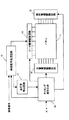
図3は本発明の実施の形態によるプラズマディスプレイ装置の回路ブロック図である。本発明の実施の形態によるプラズマディスプレイ装置は、パネル11、映像信号処理回路12、データ電極駆動回路13、走査電極駆動回路14、維持電極駆動回路15、タイミング発生回路16、点灯率検出回路17および電源回路(図示せず)を備えている。
FIG. 3 is a circuit block diagram of the plasma display apparatus according to the embodiment of the present invention. The plasma display device according to the embodiment of the present invention includes a
映像信号処理回路12は、映像信号をサブフィールド毎の映像データに変換する。データ電極駆動回路13はサブフィールドごとの映像データを各データ電極D1〜Dmに対応する信号に変換し、各データ電極D1〜Dmを駆動する。タイミング発生回路16は水平同期信号Hおよび垂直同期信号Vをもとにして各種のタイミング信号を発生し、各駆動回路ブロックに供給している。点灯率検出回路17はサブフィールド毎の映像データより各サブフィールドが全ての放電セルのうち表示発光を行う放電セルの割合を演算し、サブフィールドごとの点灯率としてタイミング発生回路16に供給する。走査電極駆動回路14はタイミング信号にもとづいて走査電極SC1〜SCnに駆動電圧波形を供給し、維持電極駆動回路15はタイミング信号にもとづいて維持電極SU1〜SUnに駆動電圧波形を供給する。
The video
本発明のプラズマディスプレイ装置においては、1フィールドを複数のサブフィールドに分割し、各サブフィールドに発光させる放電セルを選択するアドレス期間と、このアドレス期間で選択した放電セルで維持放電を行う維持期間とを設けて発光表示を行うとともに、各サブフィールドにおける維持期間に印加する維持パルスの数の重み付けを制御することにより階調制御を行っている。また、パネルの放電セルの電荷を調整するために、適宜、全ての放電セルで初期化放電を発生させる全セル初期化パルスを印加する初期化期間を設けている。 In the plasma display device of the present invention, one field is divided into a plurality of subfields, an address period for selecting discharge cells to emit light in each subfield, and a sustain period for performing sustain discharge in the discharge cells selected in this address period Are provided to perform light-emitting display, and gradation control is performed by controlling the weighting of the number of sustain pulses applied during the sustain period in each subfield. Further, in order to adjust the charge of the discharge cells of the panel, an initialization period for applying an all-cell initialization pulse for generating an initialization discharge in all the discharge cells is provided as appropriate.
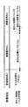
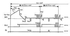
図4に、本実施の形態における映像信号による全セル初期化パルスの印加方法を示している。なお、全セル初期化パルスとは、直前の状態によらず全ての放電セルにおいて書き込み放電を安定して行うための初期化放電を生じさせるための電圧パルスであり、詳細な駆動電圧波形は後述する。また、映像信号の有無は、点灯率検出回路によって検出された各サブフィールドの点灯率によって判定される。すなわち、1フィールドにおいて1つ以上のサブフィールドの点灯率が0ではない場合は映像信号があると判定し、全てのサブフィールドの点灯率が0である場合は映像信号がなくなったと判定する。 FIG. 4 shows a method for applying an all-cell initialization pulse by a video signal in the present embodiment. The all-cell initialization pulse is a voltage pulse for generating an initialization discharge for stably performing the write discharge in all the discharge cells regardless of the immediately preceding state, and a detailed drive voltage waveform will be described later. To do. The presence / absence of the video signal is determined by the lighting rate of each subfield detected by the lighting rate detection circuit. That is, it is determined that there is a video signal when the lighting rate of one or more subfields is not 0 in one field, and it is determined that there is no video signal when the lighting rates of all subfields are 0.
図4に示すように、映像信号の有無によって、全セル初期化パルスの印加方法を切り替えるように構成するとともに、映像信号がある場合は、さらに全セル初期化パルスAを印加する状態および全セル初期化パルスBを印加する状態の2つの状態を設けている。すなわち、映像信号がある場合は、最初の1フィールドでは全セル初期化パルスAを印加する状態を配置し、そして、2フィールド目以降に全セル初期化パルスBを印加する状態を配置する。一方、映像信号がない場合は全セル初期化パルスなしの状態としている。なお、本実施の形態においては、映像信号の有無を判定するためのサブフィールドの点灯率の閾値を0と設定しているが、閾値を0以外の低い値に設定してもよい。 As shown in FIG. 4, the configuration is such that the application method of the all-cell initialization pulse is switched depending on the presence / absence of a video signal. Two states of applying the initialization pulse B are provided. That is, when there is a video signal, a state in which the all-cell initialization pulse A is applied is arranged in the first one field, and a state in which the all-cell initialization pulse B is applied in the second and subsequent fields. On the other hand, when there is no video signal, all cells are not initialized. In this embodiment, the threshold value of the lighting rate of the subfield for determining the presence or absence of the video signal is set to 0, but the threshold value may be set to a low value other than 0.
次に、それぞれの状態における駆動電圧波形とその動作について図5〜図7を用いて説明する。 Next, the driving voltage waveform and the operation in each state will be described with reference to FIGS.
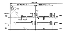
図5は、上述の全セル初期化パルスAを印加する全セル初期化期間において、パネルの各電極に印加される駆動電圧波形のうち、i行目の表示ラインを構成する走査電極および維持電極に印加する駆動電圧波形およびj列目のデータ電極に印加する駆動電圧波形を示している。 FIG. 5 shows a scan electrode and a sustain electrode constituting the i-th display line in the drive voltage waveform applied to each electrode of the panel in the all-cell initialization period in which the all-cell initialization pulse A is applied. The driving voltage waveform applied to the data electrode and the driving voltage waveform applied to the data electrode in the j-th column are shown.
全セル初期化期間の駆動電圧波形においては、1フィールドを複数のサブフィールドに分割し、それぞれのサブフィールドは初期化期間、書込み期間、維持期間を有している。 In the drive voltage waveform in the all-cell initialization period, one field is divided into a plurality of subfields, and each subfield has an initialization period, an address period, and a sustain period.
第1サブフィールドの初期化期間では、データ電極Djおよび維持電極SUiを0(V)に保持し、走査電極SCiに対して放電開始電圧以下となる電圧(Va−Vsc)から放電開始電圧を超える電圧Vr1に向かって上りランプ期間Tr1の間だけ緩やかに上昇するランプ電圧を印加する。すると、全ての放電セルにおいて1回目の微弱な初期化放電を起こし、走査電極SCi上に負の壁電圧が蓄えられるとともに維持電極SUi上およびデータ電極Dj上に正の壁電圧が蓄えられる。ここで、電極上の壁電圧とは電極を覆う誘電体層や蛍光体層上等に蓄積した壁電荷により生じる電圧を指す。この第1サブフィールドの初期化パルスは、全ての放電セルに初期化放電を発生させるため、全セル初期化パルスと呼ばれる。 In the initializing period of the first subfield, the data electrode Dj and the sustain electrode SUi are held at 0 (V), and exceed the discharge start voltage from a voltage (Va−Vsc) that is equal to or lower than the discharge start voltage with respect to the scan electrode SCi. A ramp voltage that gradually rises during the up-ramp period Tr1 toward the voltage Vr1 is applied. Then, the first weak setup discharge is caused in all the discharge cells, negative wall voltage is stored on scan electrode SCi, and positive wall voltage is stored on sustain electrode SUi and data electrode Dj. Here, the wall voltage on the electrode refers to a voltage generated by wall charges accumulated on the dielectric layer or the phosphor layer covering the electrode. The initialization pulse of the first subfield is called an all-cell initialization pulse because it generates an initialization discharge in all discharge cells.
その後、維持電極SUiを正の電圧Veに保ち、走査電極SCiに電圧Vsから電圧Vsc2に向かって緩やかに下降するランプ電圧を印加する。すると、すべての放電セルにおいて2回目の微弱な初期化放電を起こし、走査電極SCi上と維持電極SUi上との間の壁電圧が弱められ、データ電極Dj上の壁電圧も書込み動作に適した値に調整される。 Thereafter, sustain electrode SUi is maintained at positive voltage Ve, and a ramp voltage that gradually falls from voltage Vs toward voltage Vsc2 is applied to scan electrode SCi. Then, the second weak initializing discharge is caused in all the discharge cells, the wall voltage between scan electrode SCi and sustain electrode SUi is weakened, and the wall voltage on data electrode Dj is also suitable for the address operation. Adjusted to the value.
続く書込み期間では、走査電極SCiを一旦Vaに保持する。次に、その表示ラインの書き込みを行うタイミングで負の走査パルス電圧Vscを印加するとともに、データ電極Djに正の書込みパルス電圧Vdを印加する。このときデータ電極Djと走査電極SCiとの交差部の電圧は、外部印加電圧(Vd−Vsc)にデータ電極Dj上の壁電圧と走査電極SCi上の壁電圧とが加算されたものとなり、放電開始電圧を超える。そして、データ電極Djと走査電極SCiとの間および維持電極SUiと走査電極SCiとの間に書込み放電が起こり、この放電セルの走査電極SCi上に正の壁電圧が蓄積され、維持電極SUi上に負の壁電圧が蓄積され、データ電極Dj上にも負の壁電圧が蓄積される。 In the subsequent address period, scan electrode SCi is temporarily held at Va. Next, a negative scan pulse voltage Vsc is applied at the timing of writing the display line, and a positive write pulse voltage Vd is applied to the data electrode Dj. At this time, the voltage at the intersection of the data electrode Dj and the scan electrode SCi is obtained by adding the wall voltage on the data electrode Dj and the wall voltage on the scan electrode SCi to the externally applied voltage (Vd−Vsc). The starting voltage is exceeded. Then, an address discharge occurs between data electrode Dj and scan electrode SCi and between sustain electrode SUi and scan electrode SCi, and a positive wall voltage is accumulated on scan electrode SCi of this discharge cell, and on sustain electrode SUi. And a negative wall voltage is also accumulated on the data electrode Dj.
このようにして、i行目のj列目に表示すべき放電セルで書込み放電を起こして各電極上に壁電圧を蓄積する書込み動作が行われる。一方、書込みパルス電圧Vdが印加されない場合は、データ電極Djと走査電極SCiとの交差部の電圧は放電開始電圧を超えないので、書込み放電は発生しない。以上の書込み動作をn行目の放電セルに至るまで順次行った後に、書込み期間が終了する。 In this way, an address operation is performed in which an address discharge is caused in the discharge cell to be displayed in the i-th row and the j-th column and wall voltage is accumulated on each electrode. On the other hand, when the address pulse voltage Vd is not applied, the voltage at the intersection of the data electrode Dj and the scan electrode SCi does not exceed the discharge start voltage, so that address discharge does not occur. The address period ends after the above address operation is sequentially performed up to the discharge cell in the n-th row.
続く維持期間では、走査電極SCiには第1の電圧として正の維持パルス電圧Vsを、維持電極SUiには第2の電圧として接地電位、すなわち0(V)をそれぞれ印加する。このとき書込み放電を起こした放電セルにおいては、走査電極SCi上と維持電極SUi上との間の電圧は維持パルス電圧Vsに走査電極SCi上の壁電圧と維持電極SUi上の壁電圧とが加算されたものとなり、放電開始電圧を超える。そして、走査電極SCiと維持電極SUiとの間に維持放電が起こり、このとき発生した紫外線により蛍光体層が発光する。そして走査電極SCi上に負の壁電圧が蓄積され、維持電極SUi上に正の壁電圧が蓄積される。このときデータ電極Dj上にも正の壁電圧が蓄積される。 In the subsequent sustain period, a positive sustain pulse voltage Vs is applied to scan electrode SCi as the first voltage, and a ground potential, that is, 0 (V) is applied to sustain electrode SUi as the second voltage. In the discharge cell in which address discharge has occurred at this time, the voltage between scan electrode SCi and sustain electrode SUi is the sum of sustain pulse voltage Vs and the wall voltage on scan electrode SCi and the wall voltage on sustain electrode SUi. The discharge start voltage is exceeded. Then, a sustain discharge occurs between scan electrode SCi and sustain electrode SUi, and the phosphor layer emits light due to the ultraviolet rays generated at this time. Then, a negative wall voltage is accumulated on scan electrode SCi, and a positive wall voltage is accumulated on sustain electrode SUi. At this time, a positive wall voltage is also accumulated on the data electrode Dj.
書込み期間において書込み放電が起きなかった放電セルでは、維持放電は発生せず、初期化期間の終了時における壁電圧が保持される。続いて、走査電極SCiには第2の電圧である0(V)を、維持電極SUiには第1の電圧である維持パルス電圧Vsをそれぞれ印加する。すると、維持放電を起こした放電セルでは、維持電極SUi上と走査電極SCi上との間の電圧が放電開始電圧を超えるので、再び維持電極SUiと走査電極SCiとの間に維持放電が起こり、維持電極SUi上に負の壁電圧が蓄積され走査電極SCi上に正の壁電圧が蓄積される。 In the discharge cells in which no address discharge has occurred in the address period, no sustain discharge occurs, and the wall voltage at the end of the initialization period is maintained. Subsequently, 0 (V) that is the second voltage is applied to scan electrode SCi, and sustain pulse voltage Vs that is the first voltage is applied to sustain electrode SUi. Then, in the discharge cell in which the sustain discharge has occurred, the voltage between the sustain electrode SUi and the scan electrode SCi exceeds the discharge start voltage, so that the sustain discharge occurs again between the sustain electrode SUi and the scan electrode SCi, Negative wall voltage is accumulated on sustain electrode SUi, and positive wall voltage is accumulated on scan electrode SCi.
以降同様に、走査電極SCiと維持電極SUiとに交互に輝度重みに応じた数の維持パルスを印加することにより、書込み期間において書込み放電を起こした放電セルで維持放電が継続して行われる。こうして維持期間における維持動作が終了する。 Similarly, the sustain discharge is continuously performed in the discharge cells in which the address discharge is generated in the address period by alternately applying the number of sustain pulses corresponding to the luminance weight to the scan electrode SCi and the sustain electrode SUi. Thus, the maintenance operation in the maintenance period is completed.
続くサブフィールドにおける初期化期間、書込み期間、維持期間の動作も第1サブフィールドにおける動作とほぼ同様な動作で、第1サブフィールドと異なるのは、第2サブフィールドの初期化パルスPr2の電圧がVsであるため、全ての放電セルで初期化放電を起こすのではなく、直前のサブフィールドである第1サブフィールドで維持放電が発生したときのみに、初期化放電を起こすという点である。 The operations of the initialization period, address period, and sustain period in the subsequent subfield are substantially the same as the operations in the first subfield. The difference from the first subfield is the voltage of the initialization pulse Pr2 in the second subfield. Since it is Vs, initialization discharge is not caused in all discharge cells, but initialization discharge is caused only when a sustain discharge is generated in the first subfield which is the immediately preceding subfield.
図6は、上述の全セル初期化パルスの印加を停止する状態において、パネルの各電極に印加される駆動電圧波形のうち、i行目の表示ラインを構成する走査電極および維持電極に印加する駆動電圧波形およびj列目のデータ電極に印加する駆動電圧波形を示している。 FIG. 6 shows the drive voltage waveform applied to each electrode of the panel applied to the scan electrode and the sustain electrode constituting the i-th display line in a state where the application of the all-cell initialization pulse is stopped. A driving voltage waveform and a driving voltage waveform applied to the data electrode in the j-th column are shown.
全セル初期化パルスを印加しない期間の駆動電圧波形においては、1フィールドを複数のサブフィールドに分割し、第1サブフィールドは書込み期間、維持期間を有し、第2サブフィールド以降は初期化期間、書込み期間、維持期間を有している。 In the drive voltage waveform during a period in which no all-cell initialization pulse is applied, one field is divided into a plurality of subfields, the first subfield has an address period and a sustain period, and the second and subsequent subfields have an initialization period. Have a writing period and a sustaining period.
図5に示す全セル初期化期間における駆動電圧波形との違いは、第1サブフィールドの初期化期間がなくなることだけであり、全セル初期化パルスを印加しないフィールドでは、全セル初期化パルスによる初期化放電が発生せず、さらに映像信号がない場合にのみ出現するため、書き込み放電および維持放電も発生しない。よって、放電による発光が生じていない状態となる。 The only difference from the drive voltage waveform in the all-cell initializing period shown in FIG. 5 is that the initializing period of the first subfield disappears, and in the field where no all-cell initializing pulse is applied, Since the initialization discharge does not occur and appears only when there is no video signal, neither the write discharge nor the sustain discharge occurs. Therefore, no light emission due to discharge occurs.
図7は、上述の全セル初期化パルスBを印加する全セル初期化期間において、パネルの各電極に印加される駆動電圧波形のうち、i行目の表示ラインを構成する走査電極および維持電極に印加する駆動電圧波形およびj列目のデータ電極に印加する駆動電圧波形を示している。 FIG. 7 shows the scan electrodes and sustain electrodes that constitute the i-th display line in the drive voltage waveform applied to each electrode of the panel in the all-cell initialization period in which the all-cell initialization pulse B is applied. The driving voltage waveform applied to the data electrode and the driving voltage waveform applied to the data electrode in the j-th column are shown.
全セル初期化パルスBを印加する状態における駆動電圧波形は、第1サブフィールドの初期化期間以外は全セル初期化パルスAを印加する状態における駆動電圧波形と同じである。 The drive voltage waveform in the state where the all-cell initialization pulse B is applied is the same as the drive voltage waveform in the state where the all-cell initialization pulse A is applied except for the initialization period of the first subfield.
全セル初期化パルスBを印加する状態における第1サブフィールドの初期化期間では、データ電極Djおよび維持電極SUiを0(V)に保持し、走査電極SCiに対して放電開始電圧以下となる電圧(Va−Vsc)から放電開始電圧を超える電圧Vr1に向かってTr2>Tr1となるような上りランプ期間Tr2の間だけ緩やかに上昇するランプ電圧を印加する。このようにすることで、全セル初期化パルスの上りランプ期間Tr2における電圧の変化率が、全セル初期化パルスAを印加する場合に比べて小さく設定されることとなる。 In the initializing period of the first subfield in a state where all-cell initializing pulse B is applied, data electrode Dj and sustain electrode SUi are held at 0 (V), and the voltage is equal to or lower than the discharge start voltage with respect to scan electrode SCi. A ramp voltage that rises gently only during the up-ramp period Tr2 such that Tr2> Tr1 from (Va−Vsc) toward the voltage Vr1 exceeding the discharge start voltage is applied. By doing so, the rate of change of the voltage during the up-ramp period Tr2 of the all-cell initialization pulse is set smaller than when the all-cell initialization pulse A is applied.
無映像期間がある期間以上続き、全セル初期化パルスが印加されずに全く初期化放電が発生しない期間が長期間続くと、放電セル内には放電による空間電荷(プライミング粒子)がほとんどなくなってしまい、放電セルに印加される電圧が放電開始電圧を超えてから実際に放電が発生するまでの時間が長くなる。この状態で全セル初期化パルスを印加し、放電開始電圧より高い電圧までランプ電圧のように緩やかに電圧を上昇させると、放電開始電圧を超えてから放電が発生するまでの時間が通常より長くなって、放電が発生する瞬間の電圧が高くなる。このため、上昇するランプ電圧の印加中に発生する放電が強くなって強放電となり、走査電極SCiおよび維持電極SUi間に多量の異常な壁電圧が蓄えられる。この異常壁電圧によって下降するランプ電圧を印加している間においても強放電が発生して、あたかも書き込み放電が行われたのと同じような壁電圧が走査電極SCiおよび維持電極SUi上に蓄えられ、書き込みパルスを印加していなくても維持期間に誤放電が発生してしまう。この誤放電は強い異常発光となってプラズマディスプレイの表示品質を悪化させる。 If the non-video period lasts longer than a certain period, and all the cell initialization pulses are not applied and no initializing discharge is generated for a long period of time, there is almost no space charge (priming particles) due to discharge in the discharge cells. Therefore, the time from when the voltage applied to the discharge cell exceeds the discharge start voltage until the actual discharge occurs becomes longer. If the all-cell initialization pulse is applied in this state and the voltage is gradually increased like the lamp voltage to a voltage higher than the discharge start voltage, the time from when the discharge start voltage is exceeded to when discharge occurs is longer than usual. Thus, the voltage at the moment when the discharge occurs increases. For this reason, the discharge generated during the application of the rising ramp voltage becomes strong and becomes a strong discharge, and a large amount of abnormal wall voltage is stored between scan electrode SCi and sustain electrode SUi. During the application of the ramp voltage that decreases due to the abnormal wall voltage, a strong discharge occurs, and the same wall voltage as if the write discharge was performed is stored on the scan electrode SCi and the sustain electrode SUi. Even if the writing pulse is not applied, erroneous discharge occurs during the sustain period. This erroneous discharge becomes strong abnormal light emission and deteriorates the display quality of the plasma display.
本発明の実施の形態によれば、全セル初期化パルスを印加しない期間から全セル初期化パルスを印加する期間に切り替わる際に、全セル初期化パルスを印加する期間の最初のフィールドは全セル初期化パルスBを印加する状態、すなわち平均の電圧変化率が小さいランプ電圧の全セル初期化パルスを印加するため、上述のように上昇するランプ電圧を印加する際の強放電の発生が抑制され、続く維持期間における誤放電が発生しなくなるため、表示品質の悪化を防ぐことができる。このとき、全セル初期化パルスBを印加する状態における全セル初期化パルスのランプ電圧の電圧変化率を0.6V/μsec以下に設定することで、前述の強放電を抑制するのに十分な効果が得られる。 According to the embodiment of the present invention, when switching from the period in which the all-cell initialization pulse is not applied to the period in which the all-cell initialization pulse is applied, the first field of the period in which the all-cell initialization pulse is applied is Since the initialization pulse B is applied, that is, the all-cell initialization pulse having a low average voltage change rate is applied, the occurrence of strong discharge is suppressed when the rising ramp voltage is applied as described above. Further, since the erroneous discharge does not occur in the subsequent sustain period, the display quality can be prevented from deteriorating. At this time, the voltage change rate of the ramp voltage of the all-cell initialization pulse in the state where the all-cell initialization pulse B is applied is set to 0.6 V / μsec or less, which is sufficient to suppress the above-described strong discharge. An effect is obtained.
また本発明の実施の形態によれば、平均の電圧変化率が小さい全セル初期化パルスBを印加する状態の後の2番目移行のフィールドは、平均の電圧変化率が大きい全セル初期化パルスAを印加する状態とすることで、全セル初期化パルスの上りランプ期間を(Tr2−Tr1)の時間だけ短く設定することが可能となり、短縮した時間を維持パルス数の増加に充てることで、プラズマディスプレイの輝度を向上させることができ、表示性能の向上が実現できる。 Further, according to the embodiment of the present invention, the second transition field after the state in which the all-cell initialization pulse B having a small average voltage change rate is applied is the all-cell initialization pulse having a high average voltage change rate. By applying A, it becomes possible to set the up-ramp period of the all-cell initialization pulse short by the time of (Tr2-Tr1), and by using the shortened time for increasing the number of sustain pulses, The brightness of the plasma display can be improved and display performance can be improved.
上述したように、本発明の実施の形態においては、無映像期間から映像期間に切り替わる際に、電圧が緩やかに上昇する期間の平均の電圧変化率が異なる2種類以上の全セル初期化パルスを印加するように構成し、かつ前記平均の電圧変化率が大きい全セル初期化パルスを印加する期間に先立って、平均の電圧変化率が小さい全セル初期化パルスを印加する期間を配置するように構成したことにより、誤放電の発生を抑えることが可能となり、表示品位を損なうことなく高コントラストを実現できるプラズマディスプレイ装置を提供することができる。 As described above, in the embodiment of the present invention, at the time of switching from the non-video period to the video period, two or more types of all-cell initialization pulses having different average voltage change rates during the period in which the voltage rises gently. A period for applying an all-cell initialization pulse with a small average voltage change rate is arranged prior to a period for applying the all-cell initialization pulse with a high average voltage change rate. By being configured, it is possible to suppress the occurrence of erroneous discharge, and it is possible to provide a plasma display device capable of realizing high contrast without impairing display quality.
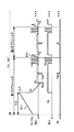
図8は、本発明の他の実施の形態による駆動波形を示している。この図8に示す実施の形態においては、全セル初期化パルスBを印加する状態における駆動電圧波形のうち、第1サブフィールドの初期化期間のみを上記実施の形態と異なる構成としたもので、それ以外は上記の実施の形態と同様な駆動電圧波形としたものである。なお、図8においては、全セル初期化パルスBを印加する状態において、パネルの各電極に印加される駆動電圧波形のうち、i行目の表示ラインを構成する走査電極および維持電極に印加する駆動電圧波形およびj列目のデータ電極に印加する駆動電圧波形を示している。 FIG. 8 shows drive waveforms according to another embodiment of the present invention. In the embodiment shown in FIG. 8, only the initialization period of the first subfield of the drive voltage waveform in a state where the all-cell initialization pulse B is applied is different from the above-described embodiment. Other than that, the drive voltage waveform is the same as that of the above embodiment. In FIG. 8, in the state where the all-cell initialization pulse B is applied, the drive voltage waveform applied to each electrode of the panel is applied to the scan electrode and the sustain electrode constituting the i-th display line. A driving voltage waveform and a driving voltage waveform applied to the data electrode in the j-th column are shown.
図8に示すように、本実施の形態においては、全セル初期化パルスBを印加する第1サブフィールドの初期化期間では、データ電極Djおよび維持電極SUiを0(V)に保持し、走査電極SCiに対して放電開始電圧以下となる電圧(Va−Vsc)から放電開始電圧を超える電圧Vr2に向かってTr3>Tr2となるような上りランプ期間Tr3の間だけ緩やかに上昇するランプ電圧を印加する。ここで、Vr2はVr1よりも高くなるように設定する。このようにすることで、全セル初期化パルスの上りランプ期間Tr2における電圧の変化率が、全セル初期化パルスAを印加する場合に比べて小さく設定できるとともに、全セル初期化パルスのピーク電圧を高くすることができる。 As shown in FIG. 8, in the present embodiment, the data electrode Dj and the sustain electrode SUi are held at 0 (V) in the initializing period of the first subfield to which the all-cell initializing pulse B is applied, and scanning is performed. A ramp voltage that rises gently only during the up-ramp period Tr3 such that Tr3> Tr2 is applied to the electrode SCi from a voltage (Va−Vsc) that is equal to or lower than the discharge start voltage toward a voltage Vr2 that exceeds the discharge start voltage. To do. Here, Vr2 is set to be higher than Vr1. In this way, the rate of change of the voltage during the up-ramp period Tr2 of the all-cell initialization pulse can be set smaller than when the all-cell initialization pulse A is applied, and the peak voltage of the all-cell initialization pulse can be set. Can be high.
すなわち、無映像期間がある期間以上続き、全セル初期化パルスが印加されずに全く初期化放電が発生しない期間が長期間続くと、前述したとおり、放電セル内には放電による空間電荷(プライミング粒子)がほとんどなくなってしまい、放電セルに印加される電圧が放電開始電圧を超えてから実際に放電が発生するまでの時間が長くなるが、同時に放電開始電圧も上昇する。この放電開始電圧の上昇が大きくなると、初期化放電が発生しない放電セルが生じ、正常な壁電圧を蓄えることができなくなるため、書き込み放電が不十分になって維持放電による表示発光が弱くなってやはり表示品質が悪化する。 In other words, if the non-video period lasts for a certain period or more and the initializing discharge is not generated at all without applying the all-cell initializing pulse, as described above, the space charge (priming by the discharge) is generated in the discharge cell. Particles) are almost lost, and the time from when the voltage applied to the discharge cell exceeds the discharge start voltage until the actual discharge occurs increases, but at the same time, the discharge start voltage also increases. When this rise in the discharge start voltage becomes large, discharge cells that do not generate initialization discharge are generated, and normal wall voltage cannot be stored. Therefore, the write discharge becomes insufficient and the display light emission due to the sustain discharge becomes weak. After all, display quality deteriorates.
本実施の形態によれば、全セル初期化パルスを印加しない期間の後の最初のフィールドを、図8に示すような全セル初期化パルスBを印加する状態、すなわち全セル初期化パルスのランプ電圧の電圧変化率を小さくするとともに、平均の電圧変化率が小さい全セル初期化パルスの電圧は、平均の電圧変化率が大きい全セル初期化パルスの電圧よりも高くすることにより、上述のような上昇するランプ電圧印加中の強放電が発生しにくくなり、さらに初期化放電が生じない放電セルをなくすことが可能となって、表示品質の悪化を防ぐことができる。このとき、全セル初期化パルスBを印加する状態における全セル初期化パルスのランプ電圧の電圧変化率を0.6V/μsec以下に設定することで、前述の強放電を抑制するのに十分な効果が得られる。 According to the present embodiment, the first field after the period in which the all-cell initialization pulse is not applied is applied to the state in which the all-cell initialization pulse B is applied as shown in FIG. As described above, the voltage change rate of the voltage is reduced and the voltage of the all-cell initialization pulse having a small average voltage change rate is set higher than the voltage of the all-cell initialization pulse having a large average voltage change rate. Thus, it is difficult to generate a strong discharge during the application of a rising lamp voltage, and it is possible to eliminate discharge cells that do not generate an initialization discharge, thereby preventing deterioration of display quality. At this time, the voltage change rate of the ramp voltage of the all-cell initialization pulse in the state where the all-cell initialization pulse B is applied is set to 0.6 V / μsec or less, which is sufficient to suppress the above-described strong discharge. An effect is obtained.
また、本実施の形態によれば、全セル初期化パルスを印加して初期化放電が発生した後には、全セル初期化パルスAを印加する状態とする、すなわち映像期間のうち、最初のフィールドにおいて平均の電圧変化率が小さい全セル初期化パルスを印加し、2番目以降のフィールドにおいて平均の電圧変化率が大きい全セル初期化パルスを印加するように構成したことにより、全セル初期化パルスの上りランプ期間を(Tr3−Tr1)の時間だけ短く設定することが可能となり、短縮した時間を維持パルス数の増加等に充てることで、プラズマディスプレイの輝度向上等による表示性能の向上が実現できる。 Further, according to the present embodiment, after the all-cell initializing pulse is applied and the initializing discharge is generated, the all-cell initializing pulse A is applied, that is, the first field in the video period. The all-cell initialization pulse having a small average voltage change rate is applied, and the all-cell initialization pulse having a large average voltage change rate is applied in the second and subsequent fields. The up-ramp period can be set shorter by the time of (Tr3-Tr1), and the display performance can be improved by improving the brightness of the plasma display by using the reduced time for increasing the number of sustain pulses. .
図9は、本発明の他の実施の形態において、全セル初期化パルスの印加方法を示すものである。 FIG. 9 shows a method for applying an all-cell initialization pulse in another embodiment of the present invention.
図9に示すように、本実施の形態においては、映像信号がない状態から映像信号がある状態に切り替わる際に、直前の無映像期間の長さを参照し、無映像期間が15秒よりも長い場合だけ、上記実施の形態で説明したように、映像信号がある映像期間において最初のフィールドで全セル初期化パルスBを印加する初期化期間を設け、その後のフィールドで全セル初期化パルスAを印加する初期化期間を設けるものである。一方、無映像期間が15秒よりも短い場合は、図9に示すように、映像信号がある状態に切り替わった直後でも全セル初期化パルスAを印加する初期化期間とする。 As shown in FIG. 9, in the present embodiment, when switching from a state in which there is no video signal to a state in which there is a video signal, the length of the previous non-video period is referred to and the non-video period is longer than 15 seconds. Only when it is long, as described in the above embodiment, an initialization period in which the all-cell initialization pulse B is applied in the first field in a certain video period is provided, and the all-cell initialization pulse A in the subsequent field. An initialization period for applying the voltage is provided. On the other hand, when the non-video period is shorter than 15 seconds, as shown in FIG. 9, it is set as the initialization period in which the all-cell initialization pulse A is applied even immediately after the video signal is switched to a certain state.
このように構成することで、無映像期間が短い場合には映像信号がある状態における最初のフィールドと2番目のフィールドとの間の輝度差による表示品質の悪化を少なくすることができ、より表示品質の高いプラズマディスプレイ装置を提供することができる。 With this configuration, when the non-video period is short, the deterioration in display quality due to the luminance difference between the first field and the second field in the state where the video signal is present can be reduced, and more display can be performed. A high-quality plasma display device can be provided.
なお、無映像期間の長さによる切り替え閾値を15秒に設定したが、これは通常の映像において、全画面黒表示の映像が続く期間がほぼ15秒以内であることと、無映像期間が3分以上続かないと、全セル初期化パルス印加時の誤放電が発生しないことから設定した値であり、15秒〜3分の間であれば、どの時間に設定しても本発明の効果は得られる。 Note that the threshold for switching according to the length of the non-video period is set to 15 seconds. This is because, in a normal video, the full-screen black display period lasts within approximately 15 seconds, and the non-video period is 3 seconds. If it does not continue for more than a minute, it is a value set because erroneous discharge does not occur at the time of applying all-cell initialization pulse, and the effect of the present invention can be set at any time as long as it is between 15 seconds and 3 minutes. can get.
図10は、図9に示す実施の形態を実施するための回路ブロック図である。図3に示す回路ブロックと異なる点は、1フィールドのうち全てのサブフィールドにおける点灯率が特定の閾値以下となる無映像期間の長さを検出する無映像期間検出手段としての無映像期間検出回路18を備えている点である。 FIG. 10 is a circuit block diagram for carrying out the embodiment shown in FIG. The difference from the circuit block shown in FIG. 3 is that a non-video period detection circuit as a non-video period detection means for detecting the length of a non-video period in which the lighting rate in all subfields of one field is below a specific threshold value. 18 is provided.
図10において、無映像期間検出回路18は、点灯率検出回路17から受け取った各サブフィールドの点灯率から、1フィールドのうち全てのサブフィールドにおける点灯率が特定の閾値以下となる無映像期間の長さを演算し、それに基づき、タイミング発生回路16の動作を制御するものである。すなわち、1フィールドのうち全てのサブフィールドにおける点灯率が特定の閾値以下となる無映像期間の長さを検出し、映像期間の直前の無映像期間の長さが特定の時間(15秒〜3分)を超えたときに、映像期間において、平均の電圧変化率が大きい全セル初期化パルスAを印加する期間に先立って、平均の電圧変化率が小さい全セル初期化パルスBを印加する期間を配置するように制御するものである。なお、全セル初期化パルスAを印加するフィールド、及び全セル初期化パルスBを印加するフィールドにおける駆動電圧波形は、上記実施の形態において説明した図5〜図8に示す駆動電圧波形と同様な波形を印加すれば、上記実施の形態で述べた作用効果と同様な作用効果を得ることができる。
In FIG. 10, the no-video
以上のように本発明は、高コントラストのプラズマディスプレイ装置を提供する上で有用な発明である。 As described above, the present invention is useful for providing a high-contrast plasma display device.
1 前面基板
2 背面基板
3 走査電極
4 維持電極
8 データ電極
11 パネル
17 点灯率検出回路
18 無映像期間検出回路
DESCRIPTION OF SYMBOLS 1 Front substrate 2 Back substrate 3 Scan electrode 4 Sustain electrode 8
Claims (7)
Priority Applications (1)
| Application Number | Priority Date | Filing Date | Title |
|---|---|---|---|
| JP2008030280A JP2009192594A (en) | 2008-02-12 | 2008-02-12 | Plasma display device |
Applications Claiming Priority (1)
| Application Number | Priority Date | Filing Date | Title |
|---|---|---|---|
| JP2008030280A JP2009192594A (en) | 2008-02-12 | 2008-02-12 | Plasma display device |
Publications (1)
| Publication Number | Publication Date |
|---|---|
| JP2009192594A true JP2009192594A (en) | 2009-08-27 |
Family
ID=41074699
Family Applications (1)
| Application Number | Title | Priority Date | Filing Date |
|---|---|---|---|
| JP2008030280A Withdrawn JP2009192594A (en) | 2008-02-12 | 2008-02-12 | Plasma display device |
Country Status (1)
| Country | Link |
|---|---|
| JP (1) | JP2009192594A (en) |
Cited By (1)
| Publication number | Priority date | Publication date | Assignee | Title |
|---|---|---|---|---|
| WO2011052219A1 (en) * | 2009-11-02 | 2011-05-05 | パナソニック株式会社 | Plasma display panel driving method and plasma display device |
-
2008
- 2008-02-12 JP JP2008030280A patent/JP2009192594A/en not_active Withdrawn
Cited By (3)
| Publication number | Priority date | Publication date | Assignee | Title |
|---|---|---|---|---|
| WO2011052219A1 (en) * | 2009-11-02 | 2011-05-05 | パナソニック株式会社 | Plasma display panel driving method and plasma display device |
| CN102598099A (en) * | 2009-11-02 | 2012-07-18 | 松下电器产业株式会社 | Plasma display panel driving method and plasma display device |
| JPWO2011052219A1 (en) * | 2009-11-02 | 2013-03-14 | パナソニック株式会社 | Plasma display panel driving method and plasma display device |
Similar Documents
| Publication | Publication Date | Title |
|---|---|---|
| JP3259766B2 (en) | Driving method of plasma display panel | |
| JP5152183B2 (en) | Plasma display device and driving method thereof | |
| JP4055740B2 (en) | Driving method of plasma display panel | |
| JP3988728B2 (en) | Driving method of plasma display panel | |
| JP2006003398A (en) | Driving method of plasma display panel | |
| US20060284796A1 (en) | Method of driving plasma display panel | |
| JP2006293112A (en) | Plasma display panel driving method and plasma display device | |
| US20070262921A1 (en) | Plasma Display Panel Drive Method and Plasma Display Device | |
| JP2008287244A (en) | Driving method of plasma display panel | |
| US20060227075A1 (en) | Plasma display panel and apparatus, and driving device and method of plasma display panel | |
| JP5044895B2 (en) | Plasma display device | |
| JP5119613B2 (en) | Driving method of plasma display panel | |
| JP2009192594A (en) | Plasma display device | |
| JP2009192593A (en) | Plasma display device | |
| JP2005338217A (en) | Plasma display panel driving method and display device | |
| JP2006308626A (en) | Driving method of plasma display panel | |
| JP4120594B2 (en) | Driving method of plasma display panel | |
| KR100761166B1 (en) | Plasma display device and driving method thereof | |
| JP2008015057A (en) | Plasma display device | |
| JP2006293206A (en) | Plasma display panel driving method and plasma display device | |
| US20090091515A1 (en) | Plasma display apparatus and related technologies | |
| KR100658395B1 (en) | Plasma display device and driving method thereof | |
| JP2006003397A (en) | Driving method of plasma display panel | |
| JP2007133291A (en) | Driving method of plasma display panel | |
| JP2008083137A (en) | Driving method of plasma display panel |
Legal Events
| Date | Code | Title | Description |
|---|---|---|---|
| A621 | Written request for application examination |
Free format text: JAPANESE INTERMEDIATE CODE: A621 Effective date: 20110126 |
|
| RD01 | Notification of change of attorney |
Free format text: JAPANESE INTERMEDIATE CODE: A7421 Effective date: 20110215 |
|
| A761 | Written withdrawal of application |
Effective date: 20121023 Free format text: JAPANESE INTERMEDIATE CODE: A761 |