JP2009200445A - Photovoltaic power-generation system - Google Patents
Photovoltaic power-generation system Download PDFInfo
- Publication number
- JP2009200445A JP2009200445A JP2008043601A JP2008043601A JP2009200445A JP 2009200445 A JP2009200445 A JP 2009200445A JP 2008043601 A JP2008043601 A JP 2008043601A JP 2008043601 A JP2008043601 A JP 2008043601A JP 2009200445 A JP2009200445 A JP 2009200445A
- Authority
- JP
- Japan
- Prior art keywords
- solar cell
- thin film
- film solar
- generation system
- power generation
- Prior art date
- Legal status (The legal status is an assumption and is not a legal conclusion. Google has not performed a legal analysis and makes no representation as to the accuracy of the status listed.)
- Pending
Links
Images




Classifications
-
- H—ELECTRICITY
- H10—SEMICONDUCTOR DEVICES; ELECTRIC SOLID-STATE DEVICES NOT OTHERWISE PROVIDED FOR
- H10F—INORGANIC SEMICONDUCTOR DEVICES SENSITIVE TO INFRARED RADIATION, LIGHT, ELECTROMAGNETIC RADIATION OF SHORTER WAVELENGTH OR CORPUSCULAR RADIATION
- H10F19/00—Integrated devices, or assemblies of multiple devices, comprising at least one photovoltaic cell covered by group H10F10/00, e.g. photovoltaic modules
- H10F19/30—Integrated devices, or assemblies of multiple devices, comprising at least one photovoltaic cell covered by group H10F10/00, e.g. photovoltaic modules comprising thin-film photovoltaic cells
- H10F19/31—Integrated devices, or assemblies of multiple devices, comprising at least one photovoltaic cell covered by group H10F10/00, e.g. photovoltaic modules comprising thin-film photovoltaic cells having multiple laterally adjacent thin-film photovoltaic cells deposited on the same substrate
-
- H—ELECTRICITY
- H02—GENERATION; CONVERSION OR DISTRIBUTION OF ELECTRIC POWER
- H02J—ELECTRIC POWER NETWORKS; CIRCUIT ARRANGEMENTS OR SYSTEMS FOR SUPPLYING OR DISTRIBUTING ELECTRIC POWER; SYSTEMS FOR STORING ELECTRIC ENERGY
- H02J3/00—Circuit arrangements for AC mains or AC distribution networks
- H02J3/38—Arrangements for feeding a single network from two or more generators or sources in parallel; Arrangements for feeding already energised networks from additional generators or sources in parallel
- H02J3/381—Dispersed generators
-
- H—ELECTRICITY
- H02—GENERATION; CONVERSION OR DISTRIBUTION OF ELECTRIC POWER
- H02S—GENERATION OF ELECTRIC POWER BY CONVERSION OF INFRARED RADIATION, VISIBLE LIGHT OR ULTRAVIOLET LIGHT, e.g. USING PHOTOVOLTAIC [PV] MODULES
- H02S50/00—Monitoring or testing of PV systems, e.g. load balancing or fault identification
- H02S50/10—Testing of PV devices, e.g. of PV modules or single PV cells
-
- H—ELECTRICITY
- H10—SEMICONDUCTOR DEVICES; ELECTRIC SOLID-STATE DEVICES NOT OTHERWISE PROVIDED FOR
- H10F—INORGANIC SEMICONDUCTOR DEVICES SENSITIVE TO INFRARED RADIATION, LIGHT, ELECTROMAGNETIC RADIATION OF SHORTER WAVELENGTH OR CORPUSCULAR RADIATION
- H10F19/00—Integrated devices, or assemblies of multiple devices, comprising at least one photovoltaic cell covered by group H10F10/00, e.g. photovoltaic modules
- H10F19/30—Integrated devices, or assemblies of multiple devices, comprising at least one photovoltaic cell covered by group H10F10/00, e.g. photovoltaic modules comprising thin-film photovoltaic cells
- H10F19/31—Integrated devices, or assemblies of multiple devices, comprising at least one photovoltaic cell covered by group H10F10/00, e.g. photovoltaic modules comprising thin-film photovoltaic cells having multiple laterally adjacent thin-film photovoltaic cells deposited on the same substrate
- H10F19/33—Patterning processes to connect the photovoltaic cells, e.g. laser cutting of conductive or active layers
-
- H—ELECTRICITY
- H10—SEMICONDUCTOR DEVICES; ELECTRIC SOLID-STATE DEVICES NOT OTHERWISE PROVIDED FOR
- H10F—INORGANIC SEMICONDUCTOR DEVICES SENSITIVE TO INFRARED RADIATION, LIGHT, ELECTROMAGNETIC RADIATION OF SHORTER WAVELENGTH OR CORPUSCULAR RADIATION
- H10F19/00—Integrated devices, or assemblies of multiple devices, comprising at least one photovoltaic cell covered by group H10F10/00, e.g. photovoltaic modules
- H10F19/70—Integrated devices, or assemblies of multiple devices, comprising at least one photovoltaic cell covered by group H10F10/00, e.g. photovoltaic modules comprising bypass diodes
-
- H—ELECTRICITY
- H10—SEMICONDUCTOR DEVICES; ELECTRIC SOLID-STATE DEVICES NOT OTHERWISE PROVIDED FOR
- H10F—INORGANIC SEMICONDUCTOR DEVICES SENSITIVE TO INFRARED RADIATION, LIGHT, ELECTROMAGNETIC RADIATION OF SHORTER WAVELENGTH OR CORPUSCULAR RADIATION
- H10F77/00—Constructional details of devices covered by this subclass
- H10F77/95—Circuit arrangements
- H10F77/953—Circuit arrangements for devices having potential barriers
- H10F77/955—Circuit arrangements for devices having potential barriers for photovoltaic devices
-
- H—ELECTRICITY
- H02—GENERATION; CONVERSION OR DISTRIBUTION OF ELECTRIC POWER
- H02J—ELECTRIC POWER NETWORKS; CIRCUIT ARRANGEMENTS OR SYSTEMS FOR SUPPLYING OR DISTRIBUTING ELECTRIC POWER; SYSTEMS FOR STORING ELECTRIC ENERGY
- H02J2101/00—Supply or distribution of decentralised, dispersed or local electric power generation
- H02J2101/20—Dispersed power generation using renewable energy sources
- H02J2101/22—Solar energy
- H02J2101/24—Photovoltaics
-
- Y—GENERAL TAGGING OF NEW TECHNOLOGICAL DEVELOPMENTS; GENERAL TAGGING OF CROSS-SECTIONAL TECHNOLOGIES SPANNING OVER SEVERAL SECTIONS OF THE IPC; TECHNICAL SUBJECTS COVERED BY FORMER USPC CROSS-REFERENCE ART COLLECTIONS [XRACs] AND DIGESTS
- Y02—TECHNOLOGIES OR APPLICATIONS FOR MITIGATION OR ADAPTATION AGAINST CLIMATE CHANGE
- Y02E—REDUCTION OF GREENHOUSE GAS [GHG] EMISSIONS, RELATED TO ENERGY GENERATION, TRANSMISSION OR DISTRIBUTION
- Y02E10/00—Energy generation through renewable energy sources
- Y02E10/50—Photovoltaic [PV] energy
- Y02E10/56—Power conversion systems, e.g. maximum power point trackers
Landscapes
- Engineering & Computer Science (AREA)
- Power Engineering (AREA)
- Photovoltaic Devices (AREA)
Abstract
【課題】太陽電池を電力変換装置に接続してなる太陽光発電システムにおいて、高効率、抵コストのシステムを提供する。
【解決手段】太陽電池モジュールが複数並列に電力変換装置に接続される太陽光発電システムであって、前記太陽電池モジュールは、前記電力変換装置の出力電圧より高電圧の電圧を出力する。
【選択図】図1In a photovoltaic power generation system in which a solar cell is connected to a power conversion device, a system with high efficiency and low cost is provided.
A solar power generation system in which a plurality of solar cell modules are connected to a power converter in parallel, and the solar cell module outputs a voltage higher than the output voltage of the power converter.
[Selection] Figure 1
Description
本発明は、太陽電池モジュールを電力変換装置に接続してなる太陽光発電システムに関する。 The present invention relates to a photovoltaic power generation system in which a solar cell module is connected to a power converter.
ウエハ状の結晶系シリコン太陽電池セルは、一枚当りの出力電圧が低く、また複数の太陽電池セルを直列接続してモジュールにしても、その出力電圧は。一般に電子機器や電機機器に供給する電圧よりも低電圧である。
そのため、複数の太陽電池モジュールを直列接続して出力電圧を高め、所望の出力電圧に設定して電力変換装置に接続することはよく知られている。例えば、特許文献1は、太陽電池モジュールを4枚直列接続した電池アレイを有する発電ブロックを住宅屋根に設置し、発電ブロックからの幹線ケーブルを接続箱に集めて並列に接続し、これをDC/AC変換装置の入力側に接続する例を示している。この特許文献1の場合、各電池モジュールの1枚あたりの発電電圧は50Vであり、これを4枚直列接続しているので、発電ブロックの出力電圧は200Vになる。
Therefore, it is well known that a plurality of solar cell modules are connected in series to increase the output voltage, set to a desired output voltage, and connected to the power converter. For example, in Patent Document 1, a power generation block having a battery array in which four solar cell modules are connected in series is installed on a house roof, and trunk cables from the power generation block are collected in a connection box and connected in parallel. An example of connection to the input side of an AC converter is shown. In the case of this Patent Document 1, the power generation voltage per battery module is 50V, and since four of these are connected in series, the output voltage of the power generation block is 200V.
そして、上記のように住宅屋根などに設置する太陽電池システムは、設置面積が様々であり、直列接続できる枚数に制限がある。また屋根面の方角や角度も様々であり、システム毎に太陽電池アレイの出力電圧は異なる。
このようなシステムごとの出力電圧の差を吸収するため、一般的なDC/AC変換装置の入力電圧は装置固有の入力範囲(例えば、80V〜380V)を持って設計され、太陽電池アレイはこの範囲に収まるように太陽電池モジュールの直列数の設定を行う。DC/AC変換装置は、様々な電圧で入力される電力を、昇圧回路によって一定の電圧(例えば、400V)に昇圧し、DC/AC変換を行っている。
しかしながら、昇圧回路を必要とする電力変換回路は、変換効率が落ちてしまうという問題点があった。
また、複数の太陽電池アレイを持つ太陽光発電システムの場合、それぞれの太陽電池アレイに昇圧回路を設け、太陽電池アレイ毎の出力電圧の差を吸収してから電力変換を行う必要があり、システムが煩雑になってコストの増大を招いていた。
本発明はこのような問題に鑑みて、太陽電池を電力変換装置に接続してなる太陽光発電システムにおいて、高効率、抵コストのシステムを提供することを目的としている。
And the solar cell system installed on a house roof etc. as mentioned above has various installation areas, and there exists a restriction | limiting in the number of sheets which can be connected in series. Also, the direction and angle of the roof surface are various, and the output voltage of the solar cell array varies from system to system.
In order to absorb such a difference in output voltage for each system, the input voltage of a general DC / AC converter is designed with a device-specific input range (for example, 80 V to 380 V), and the solar cell array is this The number of solar cell modules in series is set so as to be within the range. The DC / AC converter boosts electric power input at various voltages to a constant voltage (for example, 400 V) by a booster circuit, and performs DC / AC conversion.
However, a power conversion circuit that requires a booster circuit has a problem in that conversion efficiency decreases.
Further, in the case of a photovoltaic power generation system having a plurality of solar cell arrays, it is necessary to provide a booster circuit for each solar cell array and to perform power conversion after absorbing the difference in output voltage for each solar cell array. Has become complicated and has led to an increase in cost.
In view of such problems, an object of the present invention is to provide a high-efficiency, low-cost system in a solar power generation system in which a solar cell is connected to a power converter.
上記課題を解決するため、本発明の太陽光発電システムは、太陽電池モジュールが複数並列に電力変換装置に接続される太陽光発電システムであって、前記太陽電池モジュールは、前記電力変換装置の出力電圧より高電圧の電圧を出力する。
これにより、電力変換装置は、太陽電池モジュールの出力電圧を昇圧することなく、電力変換することにより、電力変換装置の構成が簡単になり、変換効率が高くなり、低コストのシステムを提供することができる。
In order to solve the above problems, a photovoltaic power generation system of the present invention is a photovoltaic power generation system in which a plurality of solar cell modules are connected in parallel to a power conversion device, and the solar cell module is an output of the power conversion device. A voltage higher than the voltage is output.
Accordingly, the power conversion device performs power conversion without increasing the output voltage of the solar cell module, thereby simplifying the configuration of the power conversion device, increasing the conversion efficiency, and providing a low-cost system. Can do.
本発明の太陽光発電システムは、実施形態において、前記太陽電池モジュールの出力電圧が前記電力変換装置の出力電圧の√2乃至10倍であることを特徴とする。
これにより、電力変換装置は太陽電池モジュールの出力電圧を昇圧せずに、電力変換することができ、その結果電子機器、電機機器を接続するシステム系に電源供給する事が可能になる。特に、2〜5倍であれば、より高効率になる。
In the embodiment, the photovoltaic power generation system of the present invention is characterized in that the output voltage of the solar cell module is √2 to 10 times the output voltage of the power converter.
As a result, the power conversion device can perform power conversion without increasing the output voltage of the solar cell module, and as a result, power can be supplied to the system system connecting the electronic device and the electric device. In particular, if it is 2 to 5 times, it becomes more efficient.
本発明の太陽光発電システムは、実施形態において、AC商用電力系統と連係することを特徴とする。
これにより設置条件が多様な住宅用等系統連係システムにおいてもその多様性の影響を受けずに、安定した太陽光発電システムを提供することができる。
The photovoltaic power generation system of the present invention is characterized in that it is linked to an AC commercial power system in the embodiment.
As a result, it is possible to provide a stable photovoltaic power generation system without being affected by the diversity even in a grid connection system for homes with various installation conditions.
本発明の太陽光発電システムは、実施形態において、前記太陽電池モジュールは、表面電極、光電変換層及び裏面電極をこの順に積層した複数の薄膜太陽電池素子を互いに直列接続してなる薄膜太陽電池ストリングを備えた薄膜太陽電池モジュールであることを特徴とする。
薄膜太陽電池素子は、アモルファスシリコン、微結晶シリコン、多結晶薄膜シリコンなどシリコン系薄膜太陽電池モジュール、及びCu(InGa)Se2、CdTe、CuInSe2などの化合物からなる化合物系薄膜太陽電池モジュールのように、薄膜技術を用いて製造される太陽電池素子であり、この薄膜太陽電池素子は、結晶系太陽電池、アモルファス太陽電池素子及び多結晶太陽電池素子より高電圧を出力すると共に、集積技術を用いることにより直列接続段数を多くすることにより、電子機器や電機機器に供給する電圧よりも高電圧を出力することが可能である。例えば、数100V〜1000V程度の高電圧を出力することが可能である。従って、本発明のシステムはより高い電圧で使用することができる。
In the solar power generation system of the present invention, in the embodiment, the solar cell module is a thin film solar cell string formed by connecting a plurality of thin film solar cell elements in which a front electrode, a photoelectric conversion layer, and a back electrode are laminated in this order in series. It is a thin film solar cell module provided with.
Thin-film solar cell elements include amorphous silicon, microcrystalline silicon, polycrystalline thin-film silicon and other silicon-based thin-film solar cell modules, and compound-based thin-film solar cell modules composed of compounds such as Cu (InGa) Se 2 , CdTe, and CuInSe 2 In addition, the thin film solar cell element is manufactured using a thin film technology, and the thin film solar cell element outputs a higher voltage than a crystalline solar cell, an amorphous solar cell element, and a polycrystalline solar cell element, and uses an integrated technology. Thus, by increasing the number of stages connected in series, it is possible to output a higher voltage than the voltage supplied to the electronic device or the electric device. For example, it is possible to output a high voltage of about several hundred volts to 1,000 volts. Thus, the system of the present invention can be used at higher voltages.
本発明の太陽光発電システムは、実施形態において、薄膜太陽電池モジュールを前記電力変換装置に並列接続する接続線間にそれぞれ保護部を挿入したことを特徴とする。
これにより、各薄膜太陽電池モジュールは他の薄膜太陽電池モジュールから保護され、他の薄膜太陽電池モジュールの発電出力の影響を受けない。
The photovoltaic power generation system of the present invention is characterized in that, in the embodiment, a protection unit is inserted between connection lines that connect the thin film solar cell module to the power converter in parallel.
Thereby, each thin film solar cell module is protected from other thin film solar cell modules, and is not influenced by the electric power generation output of another thin film solar cell module.
本発明の太陽光発電システムは、実施形態において、前記保護部がブロッキングダイオード、ヒューズであることを特徴とする。
これにより、各薄膜太陽電池モジュールを保護することができる。
In the photovoltaic power generation system of the present invention, in the embodiment, the protection unit is a blocking diode or a fuse.
Thereby, each thin film solar cell module can be protected.
本発明の太陽光発電システムは、実施形態において、前記複数の薄膜太陽電池モジュールを並列接続する線間にそれぞれ抵抗を接続したことを特徴とする。
これにより、各薄膜太陽電池モジュールの出力電圧を電力変換装置の入力電圧に一致させることができる。
The photovoltaic power generation system of the present invention is characterized in that, in the embodiment, a resistor is connected between lines connecting the plurality of thin film solar cell modules in parallel.
Thereby, the output voltage of each thin film solar cell module can be made to correspond with the input voltage of a power converter device.
本発明の太陽光発電システムは、実施形態において、前記抵抗は、前記電力変換装置に近い方が抵抗値が小さいことを特徴とする。
これにより、各薄膜太陽電池モジュールの出力電圧を電力変換装置の入力電圧に一致させることができる。
The photovoltaic power generation system of the present invention is characterized in that, in the embodiment, the resistance has a smaller resistance value closer to the power converter.
Thereby, the output voltage of each thin film solar cell module can be made to correspond with the input voltage of a power converter device.
本発明の太陽光発電システムは、実施形態において、前記抵抗が複数の薄膜太陽電池モジュールを前記電力変換装置に並列接続する接続線よりなることを特徴とする。
これにより、接続線の抵抗を利用して各薄膜太陽電池モジュールの出力電圧を電力変換装置の入力電圧に一致させることができる。
The photovoltaic power generation system of the present invention is characterized in that, in the embodiment, the resistor comprises a connection line that connects a plurality of thin-film solar cell modules in parallel to the power converter.
Thereby, the output voltage of each thin film solar cell module can be made to correspond with the input voltage of a power converter device using the resistance of a connection line.
本発明の太陽光発電システムは、実施形態において、前記複数の薄膜太陽電池モジュールは、前記電力変換装置に近い方が出力電圧が低いことを特徴とする。
これにより、各薄膜太陽電池モジュールの出力電力を有効に取出すことができる。
The photovoltaic power generation system of the present invention is characterized in that, in the embodiment, the plurality of thin film solar cell modules have a lower output voltage closer to the power conversion device.
Thereby, the output electric power of each thin film solar cell module can be taken out effectively.
本発明の太陽光発電システムは、実施形態において、前記薄膜太陽電池ストリングは、下記式(1)を満足する薄膜太陽電池素子の直列接続段数を有することを特徴とする。
n < Rshm / 2.5 / Vpm × Ipm + 1 ・・・(1)
ここで、Rshmは、薄膜太陽電池素子の短絡抵抗値の最頻値
Vpmは、薄膜太陽電池素子の最適動作電圧
Ipmは、薄膜太陽電池素子の最適動作電流
これにより、ホットスポット耐性を高くし、出力電圧を高くすることができる。
The photovoltaic power generation system of the present invention is characterized in that, in the embodiment, the thin film solar cell string has the number of series connection stages of thin film solar cell elements satisfying the following formula (1).
n <Rshm / 2.5 / Vpm × Ipm + 1 (1)
Here, Rshm is the mode value of the short-circuit resistance value of the thin film solar cell element.
Vpm is the optimum operating voltage for thin film solar cell elements.
Ipm is the optimum operating current of the thin-film solar cell element. As a result, the hot spot resistance can be increased and the output voltage can be increased.
本発明の太陽光発電システムは、実施形態において、前記薄膜太陽電池ストリングは、開放電圧が150Vを超えることを特徴とする。
これにより、薄膜太陽電池素子の直列接続段数適正に定めることができる。
In the embodiment, the photovoltaic power generation system of the present invention is characterized in that the thin-film solar cell string has an open-circuit voltage exceeding 150V.
Thereby, the serial connection stage number of a thin film solar cell element can be determined appropriately.
本発明に係る太陽光発電システムによれば、太陽電池を電力変換装置に複数接続してなる太陽光発電システムにおいて、高効率、低コストの太陽光発電システムが実現できる。 According to the solar power generation system according to the present invention, a high efficiency and low cost solar power generation system can be realized in a solar power generation system in which a plurality of solar cells are connected to a power converter.
(実施形態1)
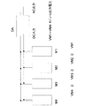
図1は、本発明の実施形態1のブロック図を示す。図1に示すように、太陽電池モジュールMは4個あり、4個の太陽電池モジュールMは並列接続されて、DC/AC変換装置DAのDC入力端に接続される。ここで、各太陽電池モジュールMは、薄膜太陽電池素子により構成され、各太陽電池モジュールMの出力電圧はDC/AC変換装置DAのAC出力電圧(実効値)より高電圧である。更に、各太陽電池モジュールMの出力電圧VMは、DC/AC変換装置DAの入力電圧より高くなるように設定される。図1は、太陽電池モジュールを4個並列接続した太陽光発電システムを示すが、太陽電池モジュールの数に制限はなく、大規模発電に必要な数の太陽電池モジュールを接続することが可能である。
(Embodiment 1)
FIG. 1 shows a block diagram of Embodiment 1 of the present invention. As shown in FIG. 1, there are four solar cell modules M, and the four solar cell modules M are connected in parallel and connected to the DC input terminal of the DC / AC converter DA. Here, each solar cell module M is comprised by a thin film solar cell element, and the output voltage of each solar cell module M is higher than the AC output voltage (effective value) of the DC / AC converter DA. Furthermore, the output voltage VM of each solar cell module M is set to be higher than the input voltage of the DC / AC converter DA. FIG. 1 shows a solar power generation system in which four solar cell modules are connected in parallel. However, the number of solar cell modules is not limited, and a number of solar cell modules necessary for large-scale power generation can be connected. .
各太陽電池モジュールMの出力電圧Vdcは、DC/AC変換装置DAのAC出力電圧(実効値)の√2倍〜数10倍程度に設定される。従って、AC出力電圧が100Vであれば、太陽電池モジュールMの出力電圧Vdcは140V〜1000Vである。またAC出力電圧が220Vであれば、太陽電池モジュールMの出力電圧Vdcは300V〜2200Vである。特に2〜5倍程度であれば、DC/AC変換装置DAの変換効率がより高くなる。この構成により、交流高電圧出力太陽光発電システムが実現できる。また本発明によれば、DC/AC変換装置へダイレクト入力が可能になる。更に、太陽電池モジュールを任意個数並列に接続するので、小規模発電システムから大規模発電システムまで、この発明を適用することができる。しかも太陽電池モジュールの出力電圧は全て等しいのが理想的であり、その場合に最大電力を取り出すことができるが、本発明は太陽電池モジュールを並列接続するので、全ての太陽電池モジュールが等しい出力電圧を出力しなくても有効に電力を取り出すことができる。従って、太陽電池モジュールの設置方向、設置条件、日射受光条件などを全く等しくする必要がなく、設置設計及び工事を容易にする。また一部の太陽電池モジュールが影になって出力電圧が低下したときも影になっていない太陽電池モジュールの出力電圧を低下させない。
これらの特徴は、特に住宅用など、設置条件が多様な太陽光発電システムにおいて有効である。
The output voltage Vdc of each solar cell module M is set to about √2 to several tens of times the AC output voltage (effective value) of the DC / AC converter DA. Therefore, if the AC output voltage is 100V, the output voltage Vdc of the solar cell module M is 140V to 1000V. If the AC output voltage is 220V, the output voltage Vdc of the solar cell module M is 300V to 2200V. In particular, if it is about 2 to 5 times, the conversion efficiency of the DC / AC converter DA becomes higher. With this configuration, an AC high voltage output solar power generation system can be realized. Further, according to the present invention, direct input to the DC / AC converter can be performed. Furthermore, since an arbitrary number of solar cell modules are connected in parallel, the present invention can be applied from a small-scale power generation system to a large-scale power generation system. Moreover, it is ideal that the output voltages of the solar cell modules are all equal, in which case the maximum power can be taken out, but since the present invention connects the solar cell modules in parallel, all the solar cell modules have the same output voltage. It is possible to effectively extract power without outputting. Therefore, there is no need to make the installation direction, installation conditions, solar light receiving conditions, etc. of the solar cell modules completely equal, and installation design and construction are facilitated. Further, even when some of the solar cell modules are shaded and the output voltage is lowered, the output voltage of the solar cell modules that are not shaded is not lowered.
These features are particularly effective in photovoltaic power generation systems with various installation conditions, such as residential use.
上記太陽電池モジュールMは、表面電極、光電変換層及び裏面電極をこの順に積層した複数の薄膜太陽電池素子を互いに直列接続してなる薄膜太陽電池ストリングを備え、次のように構成される薄膜太陽電池を用いることによって。上記に示した数百Vの高電圧が必要な太陽光発電システムを実現可能であり、住宅用等の商用電力と連係した太陽光発電システムが実現できる。
<薄膜太陽電池ストリング1> −53段×12並列×2ブロック直列の例―
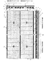
図2は、薄膜太陽電池ストリング1に係る集積型薄膜太陽電池モジュールを示し、図2(a)は平面図、図2(b)は図2(a)のA−B線断面図、図2(c)は、図2(a)のC−D線断面図を示す。図3は回路図を示す。
The solar cell module M includes a thin-film solar cell string in which a plurality of thin-film solar cell elements in which a front electrode, a photoelectric conversion layer, and a back electrode are stacked in this order are connected in series with each other, and the thin-film solar configured as follows By using a battery. The above-described solar power generation system that requires a high voltage of several hundred volts can be realized, and a solar power generation system linked to commercial power for home use can be realized.
<Thin film solar cell string 1> -Example of 53 stages x 12 parallels x 2 blocks in series-
2 shows an integrated thin film solar cell module according to the thin film solar cell string 1, FIG. 2 (a) is a plan view, FIG. 2 (b) is a cross-sectional view taken along line AB in FIG. 2 (a), FIG. (C) shows the CD sectional view taken on the line of FIG. FIG. 3 shows a circuit diagram.
薄膜太陽電池ストリング1において、支持基板1は、例えば透光性のガラス基板またはポリイミド等の樹脂基板である。その上(表面)に第1電極(例えばSnO2(酸化錫)の透明導電膜)を熱CVD法などにより形成する。第1電極は透明電極であればよく、例えばSnO2とIn2O3の混合物であるITOであってもよい。その後、透明導電膜を適宜パターニング除去して分離スクライブライン3を形成する。分離スクライブライン3を形成することにより複数に分離された第1電極2を形成する。分離スクライブライン3は、例えばレーザースクライブビームにより第1電極を溝状(スクライブライン状)に除去することにより形成される。
In the thin-film solar cell string 1, the support substrate 1 is a resin substrate such as a translucent glass substrate or polyimide. A first electrode (for example, a transparent conductive film of SnO 2 (tin oxide)) is formed thereon (surface) by a thermal CVD method or the like. The first electrode may be a transparent electrode, and may be ITO, for example, a mixture of SnO 2 and In 2 O 3 . Thereafter, the transparent conductive film is appropriately removed by patterning to form the separation scribe line 3. By forming the separation scribe line 3, the
次に、第1電極2の上に、例えばp型、i型、n型の半導体層(例えば、アモルファスシリコンまたは微結晶シリコンなど)を順次CVD法などにより成膜することにより光電変換層4を形成する。このとき、分離スクライブライン3内にも光電変換層が充填される。この光電変換層4はp-n接合であっても良いし、p-i-n接合であっても良い。また、光電変換層4は1段、2段或いは3段、またはそれ以上に積層することが可能であり、各太陽電池素子は基板側から順次長波長へ順次感度が変化するようにするとよい。このように複数の光電変換層を積層する場合、その間にコンタクト層、中間反射層などの層を挟んだ構造としてもかまわない。
複数の光電変換層4を積層する場合、各半導体層は、すべてが非晶質半導体または微結晶半導体であってもよく、また非晶質半導体または微結晶半導体の任意の組合わせであってもよい。即ち、第1光電変換層が非晶質半導体であり、第2及び第3光電変換層が微結晶半導体である積層構造、又は第1及び第2光電変換層が非晶質半導体であり、第3光電変換層が微結晶半導体である積層構造、又は第1光電変換層が微結晶半導体であり、第2及び第3光電変換層が非晶質半導体である積層構造でもよい。
Next, on the
When laminating a plurality of photoelectric conversion layers 4, all of the semiconductor layers may be amorphous semiconductors or microcrystalline semiconductors, or any combination of amorphous semiconductors or microcrystalline semiconductors. Good. That is, the first photoelectric conversion layer is an amorphous semiconductor, the second and third photoelectric conversion layers are microcrystalline semiconductors, or the first and second photoelectric conversion layers are amorphous semiconductors. A stacked structure in which the three photoelectric conversion layers are microcrystalline semiconductors or a stacked structure in which the first photoelectric conversion layer is a microcrystalline semiconductor and the second and third photoelectric conversion layers are amorphous semiconductors may be used.
また上記光電変換層4は、p-n接合またはp-i-n接合であるが、n-p接合またはn-i-p接合としてもよい。更に、p型半導体層と、i型半導体層の間にi型非晶質からなるバッファ層を備えてもよいし、なくてもよい。通常p型半導体層には、ボロン、アルミニウム等のp型不純物原子がドープされ、n型半導体層には、リン等のn型不純物原子がドープされる。i型半導体層は、完全ノンドープであっても、微量の不純物を含む弱p型又は弱n型であってもよい。
光電変換層4は、シリコンに限定されることはなく、炭素が添加されたシリコンカーバイド、またはゲルマニウムが添加されたシリコンゲルマニウムのようなシリコン系半導体、またはCu(InGa)Se2、CdTe、CuInSe2などの化合物からなる化合物系半導体によって構成することができる。
なお、薄膜太陽電池ストリング1の光電変換層4は、それぞれp-i-n接合よりなり、アモルファスシリコン/アモルファスシリコン/微結晶シリコンにより、3セルを積層した3接合型薄膜太陽電池である。
The
The
The
その後、光電変換層4に接続溝をレーザースクライブなどにより作製し、その上に第2電極(ZnO/Ag電極など)をスパッタ法などで作製する。これにより、接続溝に第2電極材料が充填され、コンタクトライン5cが形成される。これにより、コンタクトライン5cを介して、分離された光電変換層4の第2電極5と、その隣の光電変換層4の第1電極2が接続され、複数の薄膜太陽電池素子が直列接続されることになる。さらにこのコンタクトライン5cと平行にセル分離溝6をレーザースクライブなどで作製し、複数の薄膜太陽電池素子に分離する。これにより、図3の例では、個々の太陽電池素子(セル)は等しい大きさに切り離され、図3の上下方向に複数の太陽電池素子が直列接続された薄膜太陽電池ストリング(以下では、セルストリングと言うこともある。)10が作製される。
このとき、薄膜太陽電池素子の直列接続段数nが、下記式(1)の整数倍となるように分離スクライブライン3、コンタクトライン5c、セル分離溝6を形成する。即ち、セルストリングにおける薄膜太陽電池素子の直列接続の段数nを下記式(1)のようにする。
n < Rshm / 2.5 / Vpm × Ipm + 1 ・・・(1)
ここで、Rshmは、薄膜太陽電池素子の短絡抵抗値の最頻値
Vpmは、薄膜太陽電池素子の最適動作電圧
Ipmは、薄膜太陽電池素子の最適動作電流
Thereafter, a connection groove is formed in the
At this time, the separation scribe line 3, the
n <Rshm / 2.5 / Vpm × Ipm + 1 (1)
Here, Rshm is the mode value of the short-circuit resistance value of the thin film solar cell element.
Vpm is the optimum operating voltage for thin film solar cell elements.
Ipm is the optimum operating current for thin film solar cell elements.
上記構成の薄膜太陽電池モジュールは、太陽電池素子をn段集積した薄膜太陽電池ストリングが、そのうちの1段の薄膜太陽電池素子が影に隠れてホットスポット状態になった場合、薄膜太陽電池ストリングの出力は、バイパスダイオードにより短絡された状態になる。このときの等価回路は、光が当たっている(n-1)段の薄膜太陽電池素子に、光が当たっていない1段の薄膜太陽電池素子が負荷として繋がった状態になる。そのため、薄膜太陽電池ストリング内の光が当たっている部分で発電された電力は、薄膜太陽電池ストリング外部に取り出されることなく、大半が影になった薄膜太陽電池素子で消費されるようになる。この時、影になった薄膜太陽電池素子の正常部分での逆方向耐圧が十分に高い場合、薄膜太陽電池素子に流れる電流は、ゴミや傷や突起による面内の短絡部や、レーザースクライブ周辺などの低抵抗部分に流れる。
この電流の流れやすさの一つの目安として、薄膜太陽電池素子に0〜数V程度の逆電圧を印加したときの電流電圧特性から算出される短絡抵抗をRsh[Ω]とすると、この短絡抵抗Rshが上記の光が当たっている(n-1)段のセルに対して最適負荷 Rshpmとなったときがもっとも短絡部分に電力が集中する場合である。従って、短絡抵抗Rshがその値に近くならないようにモジュールを設計する必要がある。
In the thin film solar cell module having the above-described configuration, when a thin film solar cell string in which n stages of solar cell elements are integrated becomes one of the thin film solar cell elements in a shadow and is in a hot spot state, The output is shorted by the bypass diode. The equivalent circuit at this time is in a state where the (n-1) -th thin film solar cell element that is exposed to light is connected to the one-stage thin-film solar cell element that is not exposed to light as a load. Therefore, most of the electric power generated in the portion of the thin-film solar cell string that is exposed to light is consumed by the shaded thin-film solar cell element without being taken out of the thin-film solar cell string. At this time, if the reverse breakdown voltage of the normal part of the thin film solar cell element that is shaded is sufficiently high, the current flowing through the thin film solar cell element is short-circuited in the surface due to dust, scratches, or protrusions, and around the laser scribe. It flows in the low resistance part.
As one measure of the ease of current flow, if the short-circuit resistance calculated from the current-voltage characteristics when a reverse voltage of about 0 to several volts is applied to the thin-film solar cell element is Rsh [Ω], this short-circuit resistance When Rsh reaches the optimum load Rshpm for the (n-1) -stage cell that is exposed to the above light, the power is most concentrated in the short-circuited portion. Therefore, it is necessary to design the module so that the short-circuit resistance Rsh does not approach that value.
例えば、薄膜太陽電池素子1段の最適動作電圧をVpm[V]、最適動作電流をIpm[A]とし、前述のように、薄膜太陽電池素子の1段が影に隠れた場合、下記式(2)のときが最適負荷Rshpmとなり、最悪となる。
Rshpm = Vpm / Ipm × (n-1) ・・・(2)
実際の短絡抵抗Rshは、ゴミや傷や突起による面内の短絡部や、レーザースクライブ周辺の低抵抗部分など種々の原因によって生じる。これらは、製造段階の様々な理由によりばらつき、ある範囲を持って分布する。代表的なシリコン薄膜太陽電池のI-V特性から、短絡抵抗Rshがばらついた場合の短絡抵抗Rshと、そこで消費される電力Prshの関係を図4に示す。上記短絡抵抗Rshが最適負荷Rshpmからずれた場合、大体最適負荷Rshpmの2.5倍で、電力Prshが半分以下となる。即ち、図4では、最適負荷Rshpmが約330Ωのとき、電力はほぼ8Wであり、短絡抵抗Rshが130Ω、電力はほぼ4Wである。従って、短絡抵抗Rshが最適負荷Rshpmから2.5倍以上ずれたところで製造できれば、ホットスポットによる剥離の発生は大幅に低減できる。2.5倍以上ずれればよいので、最適負荷Rshpmに対して短絡負荷Rshは2.5倍以上いくらずれてもかまわない。
For example, when the optimum operating voltage of one stage of the thin film solar cell element is Vpm [V] and the optimum operating current is Ipm [A], and as described above, when one stage of the thin film solar cell element is hidden in the shadow, The case of 2) becomes the optimum load Rshpm, which is the worst.
Rshpm = Vpm / Ipm × (n-1) (2)
The actual short-circuit resistance Rsh is caused by various causes such as an in-plane short-circuit portion due to dust, scratches, or protrusions, or a low-resistance portion around the laser scribe. These vary for various reasons in the manufacturing stage and are distributed with a certain range. FIG. 4 shows the relationship between the short-circuit resistance Rsh and the power Prsh consumed when the short-circuit resistance Rsh varies from the IV characteristics of a typical silicon thin film solar cell. When the short-circuit resistance Rsh deviates from the optimum load Rshpm, the electric power Prsh is about half or less at 2.5 times the optimum load Rshpm. That is, in FIG. 4, when the optimum load Rshpm is about 330Ω, the power is about 8 W, the short-circuit resistance Rsh is 130Ω, and the power is about 4 W. Therefore, if the short-circuit resistance Rsh can be manufactured at a position deviated 2.5 times or more from the optimum load Rshpm, the occurrence of peeling due to hot spots can be greatly reduced. Since it suffices to deviate by 2.5 times or more, the short-circuit load Rsh may be shifted 2.5 times or more with respect to the optimum load Rshpm.
また、実際に作製したモジュールの短絡抵抗Rshの分布を図5に示す。薄膜太陽電池素子の短絡抵抗Rshを悪化(=低下)させる要因としては、分離スクライブラインでの分離不良、面内のゴミや突起やピンホールによる短絡、作製条件のずれによる逆方向リーク電流の増加、ドープ層の低抵抗化など、様々な事象が考えられる。しかし、主たる要因としては、短絡抵抗Rshの分布のピーク付近(〜3000Ω)では、主に分離スクライブラインでのリーク電流が短絡抵抗Rshを低下させる原因となっている。また、短絡抵抗Rshの分布のピーク付近よりも低くなる範囲では、主に面内のリーク電流が短絡抵抗Rshを低下させる原因となっている。
リーク電流の要因が面内の短絡の場合、ホットスポット現象が起きると、面内の短絡部分が剥離するかもしくは焼ききられて高抵抗になり、そのセルのF.F.を改善させるので、剥離によるIscの低下を相殺し、その結果、特性が大きく低下することは少ない。しかし、リーク電流の要因が分離スクライブラインのリーク電流の場合、ホットスポット現象が起きると、分離スクライブラインから剥離が発生し、正常な部分の太陽電池素子を巻き込んで剥離が進行したり、近くのコンタクトラインにも影響を及ぼしたりするので、面内の短絡の場合と比較すると特性も信頼性も大きく低下する。
Further, FIG. 5 shows the distribution of the short-circuit resistance Rsh of the actually manufactured module. Factors that deteriorate (= decrease) the short-circuit resistance Rsh of thin-film solar cell elements include poor separation at the scribe line, short-circuit due to in-plane dust, protrusions and pinholes, and increase in reverse leakage current due to deviations in fabrication conditions Various events are conceivable, such as lowering the resistance of the doped layer. However, as a main factor, near the peak of the distribution of the short-circuit resistance Rsh (˜3000Ω), the leakage current mainly at the separation scribe line is a cause of reducing the short-circuit resistance Rsh. Further, in the range lower than the vicinity of the peak of the distribution of the short circuit resistance Rsh, the in-plane leakage current mainly causes the short circuit resistance Rsh to decrease.
If the cause of the leakage current is an in-plane short circuit, when the hot spot phenomenon occurs, the in-plane short circuit part is peeled off or burned to increase the resistance and improve the FF of the cell. As a result, the characteristic is not greatly deteriorated. However, when the cause of the leakage current is the leakage current of the separation scribe line, when the hot spot phenomenon occurs, the separation occurs from the separation scribe line, the separation of the normal solar cell element is involved, and the separation proceeds. Since it also affects the contact line, the characteristics and reliability are greatly reduced compared to the case of in-plane short circuit.
よって、前述の最適負荷Rshpmが、分離スクライブラインのリーク電流が主要因である範囲からはずれ、面内リーク電流が主要因である範囲内にあることが望ましい。具体的には短絡抵抗Rshの最頻値をRshmとし、それに対し最適負荷Rshpmが十分に低い範囲にあればよい。最頻値Rshmが最適負荷Rshpmの2.5倍あれば、最頻値Rshmでの短絡抵抗Prshは最適負荷Rshpmでの半分程度になるので、下記式(3)となるように各パラメータを選べばよい。
Rshm > 2.5 × Rshpm = 2.5 × Vpm ÷ Ipm × (n-1) ・・・(3)
Therefore, it is desirable that the optimum load Rshpm described above is out of the range where the leakage current of the separation scribe line is the main factor and is within the range where the in-plane leakage current is the main factor. Specifically, the mode value of the short-circuit resistance Rsh may be Rshm, and the optimum load Rshpm may be in a sufficiently low range. If the mode value Rshm is 2.5 times the optimum load Rshpm, the short-circuit resistance Prsh at the mode value Rshm will be about half of the optimum load Rshpm, so each parameter should be selected so that the following equation (3) is satisfied. .
Rshm> 2.5 × Rshpm = 2.5 × Vpm ÷ Ipm × (n-1) (3)
薄膜太陽電池モジュールを構成する太陽電池素子の種類や構造や生産条件が決まると、Vpm, Ipm, Rshmはほぼ決まるので、上式(3)を変形することにより、下記のように式
(1)が求められ、これによって、ホットスポット耐性を保てる最大集積段数が決まる。
n < Rshm ÷ 2.5 ÷ Vpm × Ipm + 1 ・・・(1)
現実的には、太陽電池素子の形状にもよるが、短絡抵抗Rshはあまり低いと、太陽電池素子特性に影響が出るので、リーズナブルな太陽電池素子ではRshm > 2000Ω程度であり、Vpm/Ipm は5〜10Ω程度である。このとき、n < 80〜160となる。最適動作電圧がVpm = 1.0V程度の太陽電池素子の場合、薄膜太陽電池モジュールの最適動作電圧が80〜160V程度のものまではおのずとこの範囲に収まる。
この問題が顕著になるのはモジュールの最適動作電圧が160Vを越えた辺りからであり、その場合の対策として、前述の式(1)を守るように集積段数を決めれば良い事を、我々は見出したのである。
Vpm, Ipm, and Rshm are almost determined once the type, structure, and production conditions of the solar cell elements that make up the thin-film solar cell module are determined. By modifying equation (3) above, equation (1) This determines the maximum number of integrated stages that can maintain hot spot resistance.
n <Rshm ÷ 2.5 ÷ Vpm × Ipm + 1 (1)
In reality, depending on the shape of the solar cell element, if the short-circuit resistance Rsh is too low, the characteristics of the solar cell element will be affected. Therefore, for a reasonable solar cell element, Rshm> 2000Ω, and Vpm / Ipm is It is about 5-10Ω. At this time, n <80 to 160. In the case of a solar cell element having an optimum operating voltage of about Vpm = 1.0V, the thin film solar cell module is naturally within this range even when the optimum operating voltage is about 80 to 160V.
This problem becomes prominent when the optimum operating voltage of the module exceeds 160V, and as a countermeasure in that case, we should decide the number of integrated stages so that the above equation (1) is observed. I found it.
また、この様にして、最大集積段数が制限された場合、薄膜太陽電池モジュールとしてその集積段数で実現できる電圧出力よりも高い電圧出力を得たい場合は、薄膜太陽電池モジュール内部を複数のブロックに分けて、それぞれのブロックでの集積段数が前述の式(1)の範囲内に収まるようにし、各ブロックにバイパスダイオードを並列に取り付け、かつそれらを相互に直列接続すれば、ホットスポット耐性を確保しつつ高電圧出力の薄膜太陽電池モジュールを実現することができる。バイパスダイオードを並列に取り付けると、ホットスポットの発生時にはバイパスダイオードが作動し、ブロックの出力をほぼ短絡するので、他のブロックの影響を受けることがなくなるからである。 In addition, when the maximum number of integrated stages is limited in this way, when it is desired to obtain a voltage output higher than the voltage output that can be realized by the number of integrated stages as a thin film solar cell module, the inside of the thin film solar cell module is divided into a plurality of blocks. Separately, if the number of integrated stages in each block falls within the range of the above-mentioned formula (1), bypass diodes are attached in parallel to each block, and they are connected in series to ensure hot spot resistance. In addition, a thin-film solar cell module with a high voltage output can be realized. If the bypass diodes are mounted in parallel, the bypass diode is activated when a hot spot occurs, and the output of the block is almost short-circuited, so that it is not affected by other blocks.
さらに、この様にして作製されたセルストリング10に、図2(a)の上下方向に走るセルストリング分離溝8を作製し、セルストリング10を図2の横方向に複数に分離し、単位セルストリング10aを形成する。ここで単位セルストリングに分離するのはホットスポット耐性向上の為に、1単位セルストリング10a当りの発電量を一定値以下に抑えるためである。ホットスポット現象によるセルの損傷を抑制する観点からは単位セルストリング10aの出力Paは小さい方がよい。単位セルストリングの出力Paの上限は後述するセルホットスポット耐性試験により求められ、12Wである。単位セルストリングの出力Paは、次式(4)によって算出できる。
Pa=(P/S)×Sa ・・・(4)
Pは薄膜太陽電池モジュールの出力
Sは薄膜太陽電池モジュールの有効発電部面積
Saは単位セルストリング10aの面積
Further, a cell
Pa = (P / S) × Sa (4)
P is the output of the thin-film solar cell module S is the effective power generation area of the thin-film solar cell module Sa is the area of the
薄膜太陽電池モジュールの出力Pが一定である場合、単位セルストリング10aの出力Psを小さくするには、薄膜太陽電池モジュールに含まれる単位セルストリング10aの数を増やす、即ちストリング分割溝8の数を増やせばよい。単位セルストリング10aの出力Psの上限のみを考慮すれば、並列分割段数は多ければ多いほど有利である。しかし、並列分割段数を増やすと、以下の理由(1)〜(3)により、コンタクトライン印加電力密度(P−Ps)/Scが増大し、コンタクトライン5cが損傷されやすくなる。ここで、Pは薄膜太陽電池モジュールの出力、Psは影になったセルストリングが出力し得る出力、Scは、コンタクトライン5cの面積である。
When the output P of the thin film solar cell module is constant, in order to reduce the output Ps of the
(1)他の単位セルストリングからの印加電力の増大
1つの単位セルストリング10aが影になった場合、他の全てのセルストリングで発生した電力が影になった単位セルストリング10aに印加される。影になった単位セルストリング10aに印加される電力の値は、(P−Ps)となる。(P−Ps)の値は、単位セルストリング10aの出力Paの値が小さいほど大きくなるので、並列分割数を増やして単位セルストリング10aの出力Paを減らすと、影になった単位セルストリング10aに印加される電力が増大する。
(1) Increase in applied power from other unit cell strings When one
(2)コンタクトラインの面積減少
並列分割数を増やすと、図2(b)に示すコンタクトライン5cの長さLが短くなり、その結果、コンタクトライン5cの面積Scが小さくなる。その結果、コンタクトライン5cの抵抗値が増大する。
(2) Reduction of contact line area When the number of parallel divisions is increased, the length L of the
(3)接続溝の印加電力密度増大
上記の通り、並列分割数を増やすと、(P−Ps)の値が増大し、且つコンタクトPラインの面積Scが小さくなる。従って、コンタクトライン5cに印加される電力密度(P−Ps)/Scが増大し、コンタクトライン5cが損傷されやすくなる。
(3) Increase in applied power density of connection groove As described above, when the number of parallel divisions is increased, the value of (P-Ps) increases and the area Sc of the contact P line decreases. Therefore, the power density (P-Ps) / Sc applied to the
コンタクトライン5cの損傷を抑制するには、コンタクトライン5cに印加される電力密度(P−Ps)/Scをその上限値以下にする必要がある。コンタクトライン5cの印加電力密度(P−Ps)/Scの上限は、後述する逆方向過電流耐性試験により求まり、10.7(kW/cm2)であった。コンタクトライン印加電力密度(P−Ps)/Scは、10.7(kW/cm2)以下であれば特に限定されない。
In order to suppress the damage to the
ここで、セルホットスポット耐性試験について説明する。
まず、薄膜太陽電池ストリング1の薄膜太陽電池モジュールを作製し、5V〜8Vの逆方向電圧をかけ、逆方向電流が0.019mA/cm2〜6.44mA/cm2になるように変化させたときの電流(RB電流と言う)及びI−Vを測定する。測定したサンプルの中から、逆方向電流が異なるサンプルを並列分割して、評価対象ストリングの出力が5〜50Wになるようにする。次に、薄膜太陽電池素子(1セル)のホットスポット耐性試験を行う。ホットスポット耐性試験はICE61646 1stEDIYIONに準拠し、ここでは合格ラインを外観をよくする観点から10%より厳しくした。剥離面積は、薄膜太陽電池モジュールの基板側からサンプル表面を撮影し、膜剥離が起こった部分の面積を測定した。セルストリングの出力又はRB電流が異なるサンプルを測定した結果、RB電流が中程度の大きさの場合(0.31〜2.06mA/cm2)に膜剥離がおきやすいことが分かった。また、セルストリングの出力が12W以下の場合、RB電流の大きさによらず剥離面積は5%以下に抑えることができることが分かった。これにより、単位セルストリングの出力Psの出力は12W以下に設定された。
Here, the cell hot spot resistance test will be described.
First, when the thin film solar cell module of the thin film solar cell string 1 is manufactured, a reverse voltage of 5V to 8V is applied, and the reverse current is changed to be 0.019 mA / cm 2 to 6.44 mA / cm 2 . Current (referred to as RB current) and IV are measured. Among the measured samples, samples with different reverse currents are divided in parallel so that the output of the evaluation target string is 5 to 50 W. Next, a hot spot resistance test of the thin film solar cell element (1 cell) is performed. The hot spot resistance test conformed to ICE61646 1stEDIYION, and here, the passing line was made stricter than 10% from the viewpoint of improving the appearance. As for the peeled area, the surface of the sample was photographed from the substrate side of the thin film solar cell module, and the area of the part where the film peeled was measured. As a result of measuring samples with different cell string outputs or RB currents, it was found that when the RB current was moderate (0.31 to 2.06 mA / cm 2 ), film peeling was likely to occur. Further, it was found that when the output of the cell string is 12 W or less, the peeled area can be suppressed to 5% or less regardless of the magnitude of the RB current. As a result, the output Ps of the unit cell string is set to 12 W or less.
次に、逆方向過電流耐性試験について説明する。
まず、薄膜太陽電池ストリング1の薄膜太陽電池モジュールを作製し、発電電流の方向とは逆方向に過電流を流して、コンタクトラインの損傷を調べることにより、逆方向過電流耐性試験を行った。ここで流す電流は、IEC61730の規定に準ずると、耐過電流仕様値の1.35
倍となるが、ここでは70Vで、5.5A流した。
薄膜太陽電池モジュールに上記電圧、電流を加えると、並列接続したセルストリングに電流が分割して流れるのであるが、セルストリングの抵抗値はそれぞれ異なり、そのため電流は均等に分割されない。最悪の場合、70V、5.5A全部が1つのセルストリングに印加されることがある。この最悪の場合にもセルストリングが損傷されないかどうか試験する必要がある。そこで、コンタクトラインの幅を20μmと40μmに変化させ、長さを8.2mm〜37.5cmに変化させて、サンプルを作製し、コンタクトラインの損傷を目視判定した。その結果、コンタクトラインの面積を20μm×18cmまたは40μm×9cm=0.036cm2以上にすればよいことが分かった。セルストリングに印加した電力は、385Wであるから、385W÷0.036cm2=10.7(kW/cm2)である。
Next, a reverse overcurrent tolerance test will be described.
First, the thin film solar cell module of the thin film solar cell string 1 was produced, and the reverse overcurrent resistance test was performed by investigating the damage of the contact line by flowing an overcurrent in the direction opposite to the direction of the generated current. The current flowing here is 1.35 of the overcurrent resistance specification value according to the IEC61730 standard.
In this case, 5.5A was applied at 70V.
When the above voltage and current are applied to the thin-film solar cell module, the current flows in divided cell strings connected in parallel. However, the resistance values of the cell strings are different from each other, and thus the current is not evenly divided. In the worst case, all 70V, 5.5A may be applied to one cell string. In this worst case, it is necessary to test whether the cell string is damaged. Therefore, the width of the contact line was changed to 20 μm and 40 μm, the length was changed to 8.2 mm to 37.5 cm, a sample was prepared, and damage of the contact line was visually determined. As a result, it was found that the area of the contact line should be 20 μm × 18 cm or 40 μm × 9 cm = 0.036 cm 2 or more. Power applied to the cell string, because it is 385 W, a 385W ÷ 0.036cm 2 = 10.7 (kW / cm 2).
上記のようにして、ストリング分離溝8を形成した後、金属電極7を用いて、セルストリング10を上下二つの領域に分ける。具体的には、図2の上端に集電電極7a、下端に集電電極7bを取り付けて、垂直方向に走る分離溝8で分割した各単位セルストリングをあらためて並列に接続する。同時に、二つの集電電極7aと7bの真ん中にも中間線取り出し用の集電電極7cを追加し、ここを境に上下二つの単位ストリング10aの領域に分ける。これにより、この集積基板1は、12×2の24領域に分割される。中間線取り出し用の集電電極7cは、図2(b)に示すようにセルストリングの第2電極7の上に直接つけてもよい。あるいは、上領域と下領域の間に、中間線取り出し用電極領域を設けて集電電極7cを取り付けてもよい。
After the
この薄膜太陽電池モジュール全体の回路図を図3に示す。複数の薄膜太陽電池素子が直列接続された単位セルストリングをバイパスダイオードに並列に接続する。具体的には端子ボックス11内にバイパスダイオード12を用意し、そこに各単位セルストリング10aから導出されたリード線14、15、16を配線し、2つのセルストリングを2つのバイパスダイオード12に並列接続する。2つのバイパスダイオード12は直列接続されているため、複数の薄膜太陽電池素子が直列接続された方向に、複数のセルストリングが直列接続される。これにより、1単位ストリング内の直列接続数を式(1)に規定の段数以下に抑えつつ、その倍の電圧を端子13間に出力することを可能にしている。
上記薄膜太陽電池ストリング1は、端子ボックス11内で各単位セルストリングを接続したが、薄膜太陽電池モジュールの支持基板1上に配線を施し、この配線を用いて接続してもよい。この場合に支持基板1上に施す配線は、集電電極7の形成と同時に形成してもよく、またジャンパ線のように、別配線を用いてもよい。
A circuit diagram of the entire thin film solar cell module is shown in FIG. A unit cell string in which a plurality of thin film solar cell elements are connected in series is connected in parallel to a bypass diode. Specifically, a
In the thin film solar cell string 1, the unit cell strings are connected in the
この薄膜太陽電池ストリング1の構造で、光電変換層にアモルファスシリコン2セルと微結晶シリコン1セルを積層した3接合型のセルを用いた場合、式(1)に示した計算式は以下の様になる。
Rshm = 4000[Ω]
Vpm=1.80[V]
Ipm=62[mA]
n < Rshm ÷ 2.5 ÷ Vpm × Ipm + 1 = 56.1
よって、式(1)に従い、nは56段以下にすればよいので、薄膜太陽電池ストリング1では106段の直列構造の真ん中に中間取出し電極7cを設けて、単位セルストリング10aは、53段としている。
また、この薄膜太陽電池ストリング1では中間取り出し線7cは1本であるが、基板全体の集積段数や個々のセル電圧に応じて、分割数を増やし中間取り出し線の数を増やして1領域あたりの集積段数を減らしても良い。また、出力電圧が式(1)の段数によって得られる電圧以下である場合は、1ブロックとしてもかまわない。
In the structure of the thin-film solar cell string 1, when a three-junction type cell in which two amorphous silicon cells and one microcrystalline silicon cell are stacked is used for the photoelectric conversion layer, the calculation formula shown in the equation (1) is as follows: become.
Rshm = 4000 [Ω]
Vpm = 1.80 [V]
Ipm = 62 [mA]
n <Rshm ÷ 2.5 ÷ Vpm × Ipm + 1 = 56.1
Therefore, according to the formula (1), n may be 56 stages or less. In the thin-film solar cell string 1, the
Further, in this thin-film solar cell string 1, there is one
<薄膜太陽電池ストリング2>―53段×6並列×4ブロック直列―
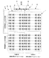
図6は、薄膜太陽電池ストリング2に係る集積型薄膜太陽電池モジュールを示し、図6(a)は平面図、図6(b)は図6(a)のE−F線断面図、図6(c)は、図6(a)のG−H線断面図を示す。図7は回路図を示す。
<Thin film
6 shows an integrated thin film solar cell module according to the thin film
薄膜太陽電池ストリング2は、より高い電圧を出力する為に、分割後の接続方法に特徴を有する。その他の構造及び作製方法は薄膜太陽電池ストリング1と同じである。具体的には、第1電極2、分離スクライブライン3、光電変換膜4、第2電極5、セル分離溝6を作製するところまでは薄膜太陽電池ストリング1と同じである。それに続いて、垂直方向に走るセルストリング分離溝8によって、12個の単位セルストリングに分割する。この分割の際に、中央のストリング分離溝8aを広めに取る。この部分には発電中に薄膜太陽電池モジュール動作電圧の2分の1に相当する高い電圧がかかる為、耐圧を確保する必要がある。この薄膜太陽電池ストリング2では、他のストリング分離溝8の2倍程度に広めに取っている。もちろん、ストリング分離溝8aに樹脂を充填したり、絶縁膜を成膜したりして絶縁耐圧を上げてもよい。
The thin film
その後、集電電極7a、7b、7cを形成する際には、それぞれ図6の右側のセルストリングと左側のセルストリングで分離し、独立電極となるように別々に形成する。これにより、53段直列接続×6並列のブロックが4つ出来上がる。これを図7に示したようにリード線21〜25を用いて端子ボックス11の内部でバイパスダイオード12に配線し、4ブロック直列接続にする。これにより、薄膜太陽電池ストリング1のさらに倍の電圧を出力する薄膜太陽電池モジュールを実現することができる。つまり、セルストリングの4倍の出力電圧が得られる。従って、複数の薄膜太陽電池素子が直列接続された方向に複数のセルストリングが直列接続され、また複数の薄膜太陽電池素子が直列接続された方向と直交する方向に複数のセルストリングが直列接続される。これにより、1単位のセルストリング内の直列接続数を式(1)に規定の段数以下に抑えつつ、その4倍の電圧を端子13間に出力することを可能にしている。
4ブロック直列接続する為の配線は、各ブロックからリード線を導出して薄膜太陽電池モジュール内で直接繋いでもいいし、図7に示すように各ブロックから導出したリード線を端子ボックス内で繋いでも、一旦モジュール外部に引き出してから直列に繋いでもかまわない。
Thereafter, when forming the collecting
The wiring for connecting 4 blocks in series may be such that lead wires are led out from each block and directly connected in the thin film solar cell module, or lead wires led out from each block are connected in the terminal box as shown in FIG. However, it may be pulled out of the module and connected in series.
また、薄膜太陽電池ストリング1と同様に、直列ブロック毎にバイパスダイオード12を並列に取り付ける。これにより、1領域内の直列接続数を式(1)に規定の段数以下に抑えつつ、その4倍の電圧を出力することを可能にしている。バイパスダイオード12は、小型薄型のものを薄膜太陽電池モジュールに内蔵してもいいし、端子ボックス内に内蔵してもいい。
この薄膜太陽電池ストリング2のように、太陽電池素子の集積方向と異なる方向、例えば直交する方向に分割し、それを接続し直すと、薄膜太陽電池ストリング1の場合のように集積方向にのみ分割した場合と違い、最適な集積ピッチを保ったまま高電圧化することができ、モジュール変換効率を落とすことなく高電圧化することができる。
Similarly to the thin film solar cell string 1, the
As in the thin film
<薄膜太陽電池ストリング3>―48段×5並列×2ブロック直列の基板を2枚用いて48段×5並列×4ブロック直列を実現した例―
薄膜太陽電池ストリング1と2では支持基板そのものが大きく、その上に全てのセルストリングを形成した薄膜太陽電池モジュールの例を示したが、小さな支持基板を複数組み合わせて大きな太陽電池モジュールを作る場合にも同様の課題に直面する。その場合、個々の支持基板内のセルストリングを式(1)に示した条件を満たす様に形成し、それらを繋ぎ合わせれば信頼性を確保しつつ高電圧のモジュールを作製できる。即ち、セルストリングは、薄膜太陽電池ストリング1及び2と同じようにして構成し、これを図8に示すように、小型集積基板2枚をひとつの集積基板9上で、並列接続する。すなわち、図8に示すように、2つの薄膜太陽電池モジュールの支持基板1を、1つのカバーガラスからなる集積基板9上に載置し、一つにまとめるように構成する。これを図9に示すように端子ボックス11内で、直列接続する。
上記小さい支持基板は、それぞれ個別に封止して、それらを図8に示すように集積基板上に一体化してもよいし、または枠を用いて一体化してもよい。また、上記のように2つの小さい支持基板を1つの集積基板上に載置して、それらをひとつに纏めるように封止してもよい。
また、二つの支持基板を別々に封止し、枠でまとめてひとつの薄膜太陽電池モジュールにしてもよい。
<Thin Film Solar Cell String 3> -Example of 48-stage x 5-parallel x 4-block series using two 48-stage x 5-parallel x 2-block series substrates-
In the thin film
The small support substrates may be individually sealed and integrated on the integrated substrate as shown in FIG. 8, or may be integrated using a frame. Further, as described above, two small supporting substrates may be placed on one integrated substrate and sealed so that they are combined into one.
Alternatively, the two support substrates may be sealed separately and combined into a frame to form one thin film solar cell module.
以上に示した薄膜太陽電池ストリング1〜3は、スーパーストレート型構造の薄膜太陽電池モジュールについて説明したが、薄膜太陽電池モジュールはサブストレート型構造にも適用可能であり、その場合、基板上に第2電極、光電変換層及び第1電極を、この順に形成する。
また、上記薄膜太陽電池ストリング1〜3は、端子ボックスを1つ備えるが、端子ボックスを複数備え、複数の端子ブック間を配線することによりセルストリングを直列接続してもよい。
また、上記薄膜太陽電池ストリング1〜3は、セルストリングを2個形成して2分割したが、出力電圧がセルストリングの段数nによって満足できるときは、1個であってもよい。また、セルストリングは、偶数個でなく奇数個であってもよい。
また、上記薄膜太陽電池ストリング1〜3は、バイパスダイオードに接続して、セルストリングを直列接続したが、バイパスダイオードをなくしてセルストリングを直接接続してもよいし、バイパスダイオードに代えて抵抗、負荷に接続してもよい。
The thin film solar cell strings 1 to 3 described above have been described for the super straight type thin film solar cell module. However, the thin film solar cell module can also be applied to a substrate type structure. Two electrodes, a photoelectric conversion layer, and a first electrode are formed in this order.
Moreover, although the said thin film solar cell strings 1-3 are provided with one terminal box, you may provide a plurality of terminal boxes and connect a cell string in series by wiring between several terminal books.
Moreover, although the said thin film solar cell strings 1-3 formed two cell strings and divided into two, when the output voltage can be satisfied with the stage number n of a cell string, one may be sufficient. The cell string may be an odd number instead of an even number.
The thin film solar cell strings 1 to 3 are connected to the bypass diode and connected in series with the cell string. However, the cell string may be directly connected without the bypass diode, or a resistor, It may be connected to a load.
(実施形態2)
図10は、太陽光発電システムの実施形態2のブロック図を示す。図10に示すように、薄膜太陽電池モジュールMは、DC/AC変換装置DAに並列接続する接続線K1、K2に対して、それぞれ保護部BDを挿入したことを特徴とする。保護部BDは、ブロッキングダイオード、ヒューズである。これ以外に、薄膜太陽電池モジュールMを他の薄膜太陽電池モジュールから保護する機能素子を用いてもよい。その他の構成は、実施形態1と同様である。薄膜太陽電池モジュールを形成する薄膜太陽電池ストリング1〜3も実施形態1と同様である。
これにより、各薄膜太陽電池モジュールMは独立し、他の薄膜太陽電池モジュールMの影響を受けない。即ち、1つの太陽電池モジュールが影になり出力電圧が低下しても出力電圧が低下した太陽電池モジュールに逆流することがない。
(Embodiment 2)
FIG. 10 shows a block diagram of
Thereby, each thin film solar cell module M becomes independent, and is not influenced by the other thin film solar cell module M. That is, even if one solar cell module is shaded and the output voltage decreases, it does not flow backward to the solar cell module whose output voltage has decreased.
(実施形態3)
図11は、太陽光発電システムの実施形態3のブロック図を示す。図11に示すように各薄膜太陽電池モジュールMを並列接続する接続線K1、K2の各間にそれぞれ抵抗R1、R2、R3、R4を接続する。抵抗R1、R2、R3、R4は、DC/AC変換装置DAに近い方が抵抗値が小さくなるようにする。また、抵抗R1、R2、R3、R4は、接続線K1及びK2の内部抵抗により形成することができる。図11の抵抗R1、R2、R3、R4は接続線K1、K2にそれぞれ接続したが、接続線K1またはK2のいずれか一方であってもかまわない。また接続線K1、K2の内部抵抗により抵抗R1、R2、R3、R4を形成する場合、必要に応じて接続線K1及びK2の線の太さを変えたり、線の数を変えたりするとよい。この抵抗R1、R2、R3、R4により、DC/AC変換装置DAの入力端で等しい電圧になるようにする。
その他の構成は、実施形態1と同様である。薄膜太陽電池モジュールを形成する薄膜太陽電池ストリング1〜3も実施形態1と同様である。
(Embodiment 3)
FIG. 11: shows the block diagram of Embodiment 3 of a solar energy power generation system. As shown in FIG. 11, resistors R1, R2, R3, and R4 are connected between connection lines K1 and K2 that connect the thin film solar cell modules M in parallel, respectively. The resistors R1, R2, R3, and R4 are set to have a resistance value that is closer to the DC / AC converter DA. Further, the resistors R1, R2, R3, and R4 can be formed by internal resistances of the connection lines K1 and K2. The resistors R1, R2, R3, and R4 in FIG. 11 are connected to the connection lines K1 and K2, respectively, but may be either the connection line K1 or K2. When the resistors R1, R2, R3, and R4 are formed by the internal resistances of the connection lines K1 and K2, the thicknesses of the connection lines K1 and K2 may be changed or the number of lines may be changed as necessary. The resistors R1, R2, R3, and R4 make the voltage equal at the input terminal of the DC / AC converter DA.
Other configurations are the same as those of the first embodiment. The thin film solar cell strings 1 to 3 forming the thin film solar cell module are the same as those in the first embodiment.
(実施形態4)
図12は、太陽光発電システムの実施形態4のブロック図を示す。図12に示すように複数の薄膜太陽電池モジュールMは、DC/AC変換装置DAに遠い方が出力電圧が高く、近い方が出力電圧が低くなるようにする。そして、DC/AC変換装置DAの入力端で等しい電圧になるようにする。複数の薄膜太陽電池モジュールMの出力電圧にバラツキがあるとき、出力電圧の順に並べ、出力電圧の低い薄膜太陽電池モジュールMがDC/AC変換装置DAの入力端になるように配置するとよい。
その他の構成は、実施形態1と同様である。薄膜太陽電池モジュールを形成する薄膜太陽電池ストリング1〜3も実施形態1と同様である。
実施形態1〜4では、電力変換装置としてDC/AC変換回路を用いた例で説明しているが、本発明の効果はDC/AC変換回路に限るものではない。例えば、DC/AC変換回路を電力変換回路に用いた太陽光発電システムでも、同様の効果が得られる。
(Embodiment 4)
FIG. 12: shows the block diagram of
Other configurations are the same as those of the first embodiment. The thin film solar cell strings 1 to 3 forming the thin film solar cell module are the same as those in the first embodiment.
In the first to fourth embodiments, an example in which a DC / AC conversion circuit is used as the power conversion device is described. However, the effect of the present invention is not limited to the DC / AC conversion circuit. For example, the same effect can be obtained even in a solar power generation system using a DC / AC conversion circuit as a power conversion circuit.
M1M2,M3,M4 薄膜太陽電池モジュール
DA DA/AC変換装置
BD 保護部
R1,R2,R3,R4 抵抗
VM1,VM2,VM3、VM4 薄膜太陽電池モジュールの出力電圧
M1M2, M3, M4 Thin Film Solar Cell Module DA DA / AC Converter BD Protection Units R1, R2, R3, R4 Resistors VM1, VM2, VM3, VM4 Output Voltage of Thin Film Solar Cell Module
Claims (12)
n < Rshm / 2.5 / Vpm × Ipm + 1 ・・・(1)
ここで、Rshmは、薄膜太陽電池素子の短絡抵抗値の最頻値
Vpmは、薄膜太陽電池素子の最適動作電圧
Ipmは、薄膜太陽電池素子の最適動作電流 The said thin film solar cell string is a solar power generation system of Claim 4 which has the number of serial connection stages of the thin film solar cell element which satisfies following formula (1).
n <Rshm / 2.5 / Vpm × Ipm + 1 (1)
Here, Rshm is the mode value of the short-circuit resistance value of the thin film solar cell element.
Vpm is the optimum operating voltage for thin film solar cell elements.
Ipm is the optimum operating current for thin film solar cell elements.
Priority Applications (3)
| Application Number | Priority Date | Filing Date | Title |
|---|---|---|---|
| JP2008043601A JP2009200445A (en) | 2008-02-25 | 2008-02-25 | Photovoltaic power-generation system |
| EP09714008A EP2249394A4 (en) | 2008-02-25 | 2009-02-23 | PHOTOVOLTAIC POWER SYSTEM |
| PCT/JP2009/053197 WO2009107584A1 (en) | 2008-02-25 | 2009-02-23 | Photovoltaic power system |
Applications Claiming Priority (1)
| Application Number | Priority Date | Filing Date | Title |
|---|---|---|---|
| JP2008043601A JP2009200445A (en) | 2008-02-25 | 2008-02-25 | Photovoltaic power-generation system |
Publications (1)
| Publication Number | Publication Date |
|---|---|
| JP2009200445A true JP2009200445A (en) | 2009-09-03 |
Family
ID=41015978
Family Applications (1)
| Application Number | Title | Priority Date | Filing Date |
|---|---|---|---|
| JP2008043601A Pending JP2009200445A (en) | 2008-02-25 | 2008-02-25 | Photovoltaic power-generation system |
Country Status (3)
| Country | Link |
|---|---|
| EP (1) | EP2249394A4 (en) |
| JP (1) | JP2009200445A (en) |
| WO (1) | WO2009107584A1 (en) |
Cited By (6)
| Publication number | Priority date | Publication date | Assignee | Title |
|---|---|---|---|---|
| WO2011052479A1 (en) * | 2009-10-30 | 2011-05-05 | 三洋電機株式会社 | Photoelectric conversion module |
| JP2012146729A (en) * | 2011-01-07 | 2012-08-02 | Sony Corp | Solar power generation module and solar power generation system |
| JP2013506988A (en) * | 2009-09-30 | 2013-02-28 | エルジー イノテック カンパニー リミテッド | Solar power plant |
| KR101370676B1 (en) * | 2012-10-30 | 2014-03-07 | 주식회사 탑선 | Solar battery module |
| JP2016531537A (en) * | 2013-07-10 | 2016-10-06 | サン−ゴバン グラス フランス | SOLAR MODULE HAVING ELECTRIC INSULATION MODULE SUPPORT AND METHOD FOR PRODUCING THE SAME |
| JP2017509288A (en) * | 2014-03-28 | 2017-03-30 | サンパワー コーポレイション | High voltage solar module |
Families Citing this family (5)
| Publication number | Priority date | Publication date | Assignee | Title |
|---|---|---|---|---|
| GB2522408A (en) | 2014-01-14 | 2015-07-29 | Ibm | Monolithically integrated thin-film device with a solar cell, an integrated battery and a controller |
| JP6677087B2 (en) * | 2016-06-08 | 2020-04-08 | 三菱ケミカル株式会社 | Solar cell module |
| EP3648173B1 (en) * | 2018-10-30 | 2023-05-24 | IMEC vzw | Thin-film photovoltaic module with integrated electronics and methods for manufacturing thereof |
| DE102020128080B4 (en) | 2020-10-26 | 2022-07-14 | Fraunhofer-Gesellschaft zur Förderung der angewandten Forschung eingetragener Verein | solar cell module |
| DE102021103099A1 (en) * | 2021-02-10 | 2022-08-11 | Hanwha Q Cells Gmbh | Photovoltaic module and a method for its manufacture |
Citations (3)
| Publication number | Priority date | Publication date | Assignee | Title |
|---|---|---|---|---|
| JPH08185235A (en) * | 1994-12-27 | 1996-07-16 | Sharp Corp | Photovoltaic power generation system with solar cell module abnormality check function |
| JP2001068713A (en) * | 1999-08-25 | 2001-03-16 | Kanegafuchi Chem Ind Co Ltd | Thin-film photoelectric conversion module |
| JP2004094660A (en) * | 2002-08-30 | 2004-03-25 | Sharp Corp | Photovoltaic power generation device design support device and photovoltaic power generation device design method |
Family Cites Families (7)
| Publication number | Priority date | Publication date | Assignee | Title |
|---|---|---|---|---|
| JP3554116B2 (en) * | 1996-09-06 | 2004-08-18 | キヤノン株式会社 | Power control device and solar power generation system using the same |
| US6856654B1 (en) * | 1997-09-15 | 2005-02-15 | Research In Motion Limited | Power supply system for a packet-switched radio transmitter |
| AU5400501A (en) * | 2000-06-27 | 2002-01-03 | Canon Kabushiki Kaisha | Photovoltaic element, producing method therefor, and solar cell modules |
| US6750394B2 (en) * | 2001-01-12 | 2004-06-15 | Sharp Kabushiki Kaisha | Thin-film solar cell and its manufacturing method |
| DE10136147B4 (en) * | 2001-07-25 | 2004-11-04 | Kolm, Hendrik, Dipl.-Ing. | Photovoltaic alternator |
| US8013583B2 (en) * | 2004-07-01 | 2011-09-06 | Xslent Energy Technologies, Llc | Dynamic switch power converter |
| DE102004044425B4 (en) * | 2004-09-14 | 2012-11-22 | Sielaff Gmbh & Co. Kg Automatenbau | Vending machine with charging function for local energy source |
-
2008
- 2008-02-25 JP JP2008043601A patent/JP2009200445A/en active Pending
-
2009
- 2009-02-23 EP EP09714008A patent/EP2249394A4/en not_active Withdrawn
- 2009-02-23 WO PCT/JP2009/053197 patent/WO2009107584A1/en not_active Ceased
Patent Citations (3)
| Publication number | Priority date | Publication date | Assignee | Title |
|---|---|---|---|---|
| JPH08185235A (en) * | 1994-12-27 | 1996-07-16 | Sharp Corp | Photovoltaic power generation system with solar cell module abnormality check function |
| JP2001068713A (en) * | 1999-08-25 | 2001-03-16 | Kanegafuchi Chem Ind Co Ltd | Thin-film photoelectric conversion module |
| JP2004094660A (en) * | 2002-08-30 | 2004-03-25 | Sharp Corp | Photovoltaic power generation device design support device and photovoltaic power generation device design method |
Non-Patent Citations (1)
| Title |
|---|
| JPN6009012553; 江口政樹 他: '住宅用太陽光発電システム用ストリングパワーコンディショナ' シャープ技報 第83号, 200208, 63-64 * |
Cited By (11)
| Publication number | Priority date | Publication date | Assignee | Title |
|---|---|---|---|---|
| JP2013506988A (en) * | 2009-09-30 | 2013-02-28 | エルジー イノテック カンパニー リミテッド | Solar power plant |
| US9595913B2 (en) | 2009-09-30 | 2017-03-14 | Lg Innotek Co., Ltd. | Solar cell apparatus |
| WO2011052479A1 (en) * | 2009-10-30 | 2011-05-05 | 三洋電機株式会社 | Photoelectric conversion module |
| CN102473758A (en) * | 2009-10-30 | 2012-05-23 | 三洋电机株式会社 | Photoelectric conversion module |
| JP2012146729A (en) * | 2011-01-07 | 2012-08-02 | Sony Corp | Solar power generation module and solar power generation system |
| KR101370676B1 (en) * | 2012-10-30 | 2014-03-07 | 주식회사 탑선 | Solar battery module |
| JP2016531537A (en) * | 2013-07-10 | 2016-10-06 | サン−ゴバン グラス フランス | SOLAR MODULE HAVING ELECTRIC INSULATION MODULE SUPPORT AND METHOD FOR PRODUCING THE SAME |
| JP2017509288A (en) * | 2014-03-28 | 2017-03-30 | サンパワー コーポレイション | High voltage solar module |
| JP2021044560A (en) * | 2014-03-28 | 2021-03-18 | サンパワー コーポレイション | High voltage solar modules |
| JP7055952B2 (en) | 2014-03-28 | 2022-04-19 | サンパワー コーポレイション | Photovoltaic module |
| US11811360B2 (en) | 2014-03-28 | 2023-11-07 | Maxeon Solar Pte. Ltd. | High voltage solar modules |
Also Published As
| Publication number | Publication date |
|---|---|
| WO2009107584A1 (en) | 2009-09-03 |
| EP2249394A4 (en) | 2012-10-24 |
| EP2249394A1 (en) | 2010-11-10 |
Similar Documents
| Publication | Publication Date | Title |
|---|---|---|
| JP2009200445A (en) | Photovoltaic power-generation system | |
| JP5396382B2 (en) | Power line for solar power generation system and solar power generation system using the same | |
| JPWO2009104601A1 (en) | Thin film solar cell module | |
| US10074755B2 (en) | High efficiency solar panel | |
| CN106165116B (en) | Photovoltaic module with bypass diode | |
| CN106159020B (en) | Use the two-sided photovoltaic module of heterojunction solar battery | |
| CN204538036U (en) | Solar panel, solar cell, solar cell panel assembly and solar battery apparatus | |
| CN203339197U (en) | Photovoltaic module | |
| US20160226438A1 (en) | Solar module with diode device for shading | |
| US20170170336A1 (en) | Systems and methods for routing wires in a solar module | |
| US20190371950A1 (en) | Configurable solar cells | |
| CN101593781A (en) | Non-linear solar cell module | |
| CN115084300A (en) | Single thin film photovoltaic cell, photovoltaic cell panel and manufacturing method thereof | |
| US20110011439A1 (en) | Photovoltaic power system | |
| US20240222537A1 (en) | Arrangements of Substrings in Photovoltaic Modules | |
| CN114946040A (en) | Light capturing dynamic photovoltaic module | |
| CN106788218A (en) | A kind of many terminal box solar components | |
| US20250040258A1 (en) | Two-terminal tandem solar module | |
| JP7646062B1 (en) | Solar power generation system installation method and solar power generation system | |
| CN108172650A (en) | New solar photovoltaic components and building photovoltaic integrated components | |
| CN121358055A (en) | Solar cells, battery modules and photovoltaic systems | |
| CN121013493A (en) | Solar cells, battery modules and photovoltaic systems | |
| KR101350749B1 (en) | Photovoltaic Module | |
| Kurtz et al. | Opportunities and Challenges for Power Electronics in PV Modules (Presentation) |
Legal Events
| Date | Code | Title | Description |
|---|---|---|---|
| A621 | Written request for application examination |
Free format text: JAPANESE INTERMEDIATE CODE: A621 Effective date: 20100218 |
|
| A131 | Notification of reasons for refusal |
Free format text: JAPANESE INTERMEDIATE CODE: A131 Effective date: 20120717 |
|
| A521 | Request for written amendment filed |
Free format text: JAPANESE INTERMEDIATE CODE: A523 Effective date: 20120911 |
|
| A02 | Decision of refusal |
Free format text: JAPANESE INTERMEDIATE CODE: A02 Effective date: 20121204 |
|
| A521 | Request for written amendment filed |
Free format text: JAPANESE INTERMEDIATE CODE: A523 Effective date: 20130221 |
|
| A911 | Transfer to examiner for re-examination before appeal (zenchi) |
Free format text: JAPANESE INTERMEDIATE CODE: A911 Effective date: 20130228 |
|
| A912 | Re-examination (zenchi) completed and case transferred to appeal board |
Free format text: JAPANESE INTERMEDIATE CODE: A912 Effective date: 20130502 |
|
| A912 | Re-examination (zenchi) completed and case transferred to appeal board |
Free format text: JAPANESE INTERMEDIATE CODE: A912 Effective date: 20130524 |