JP2009201541A - Imaging system and endoscopic system - Google Patents
Imaging system and endoscopic system Download PDFInfo
- Publication number
- JP2009201541A JP2009201541A JP2008043826A JP2008043826A JP2009201541A JP 2009201541 A JP2009201541 A JP 2009201541A JP 2008043826 A JP2008043826 A JP 2008043826A JP 2008043826 A JP2008043826 A JP 2008043826A JP 2009201541 A JP2009201541 A JP 2009201541A
- Authority
- JP
- Japan
- Prior art keywords
- signal line
- solid
- reset
- connection state
- unit
- Prior art date
- Legal status (The legal status is an assumption and is not a legal conclusion. Google has not performed a legal analysis and makes no representation as to the accuracy of the status listed.)
- Pending
Links
- 238000003384 imaging method Methods 0.000 title claims abstract description 69
- 238000000605 extraction Methods 0.000 claims abstract description 38
- 230000002159 abnormal effect Effects 0.000 claims abstract description 16
- 238000006243 chemical reaction Methods 0.000 claims abstract description 11
- 238000005286 illumination Methods 0.000 claims description 14
- 239000000284 extract Substances 0.000 abstract description 5
- 238000003780 insertion Methods 0.000 description 13
- 230000037431 insertion Effects 0.000 description 13
- 238000005452 bending Methods 0.000 description 9
- 238000000034 method Methods 0.000 description 9
- 238000012545 processing Methods 0.000 description 9
- 238000001514 detection method Methods 0.000 description 8
- 230000005856 abnormality Effects 0.000 description 6
- 239000004020 conductor Substances 0.000 description 6
- 230000003287 optical effect Effects 0.000 description 6
- 230000000875 corresponding effect Effects 0.000 description 5
- 230000000630 rising effect Effects 0.000 description 5
- XLYOFNOQVPJJNP-UHFFFAOYSA-N water Substances O XLYOFNOQVPJJNP-UHFFFAOYSA-N 0.000 description 5
- 230000008569 process Effects 0.000 description 4
- 239000000523 sample Substances 0.000 description 4
- 239000000872 buffer Substances 0.000 description 3
- 238000001444 catalytic combustion detection Methods 0.000 description 3
- 238000010586 diagram Methods 0.000 description 3
- 230000009471 action Effects 0.000 description 2
- 239000003990 capacitor Substances 0.000 description 2
- 238000012937 correction Methods 0.000 description 2
- 230000002596 correlated effect Effects 0.000 description 2
- 239000006059 cover glass Substances 0.000 description 2
- 239000011159 matrix material Substances 0.000 description 2
- 230000007246 mechanism Effects 0.000 description 2
- 238000005070 sampling Methods 0.000 description 2
- 125000006850 spacer group Chemical group 0.000 description 2
- 238000012546 transfer Methods 0.000 description 2
- 239000000853 adhesive Substances 0.000 description 1
- 230000001070 adhesive effect Effects 0.000 description 1
- 230000008859 change Effects 0.000 description 1
- 239000002131 composite material Substances 0.000 description 1
- 230000008878 coupling Effects 0.000 description 1
- 238000010168 coupling process Methods 0.000 description 1
- 238000005859 coupling reaction Methods 0.000 description 1
- 230000006378 damage Effects 0.000 description 1
- 230000003247 decreasing effect Effects 0.000 description 1
- 238000009792 diffusion process Methods 0.000 description 1
- 239000000428 dust Substances 0.000 description 1
- 230000000694 effects Effects 0.000 description 1
- 229910052736 halogen Inorganic materials 0.000 description 1
- 150000002367 halogens Chemical class 0.000 description 1
- 230000020169 heat generation Effects 0.000 description 1
- 238000002347 injection Methods 0.000 description 1
- 239000007924 injection Substances 0.000 description 1
- 230000004048 modification Effects 0.000 description 1
- 238000012986 modification Methods 0.000 description 1
- 239000004065 semiconductor Substances 0.000 description 1
- 229910052724 xenon Inorganic materials 0.000 description 1
- FHNFHKCVQCLJFQ-UHFFFAOYSA-N xenon atom Chemical compound [Xe] FHNFHKCVQCLJFQ-UHFFFAOYSA-N 0.000 description 1
Images




Landscapes
- Instruments For Viewing The Inside Of Hollow Bodies (AREA)
- Endoscopes (AREA)
Abstract
Description
本発明は、固体撮像素子と外部装置とが信号線を介して電気的に接続された撮像システム及び内視鏡システムに関するものである。 The present invention relates to an imaging system and an endoscope system in which a solid-state imaging device and an external device are electrically connected via a signal line.
内視鏡システムは、体腔内(被検体内)を撮像する固体撮像素子を備えた内視鏡と、固体撮像素子の動作を制御するとともに、固体撮像素子の出力信号を受信して画像を生成する外部装置(プロセッサ装置)とを備えた一種の撮像システムである。この固体撮像素子と外部装置とは、複数の信号線によって電気的に接続されており、これら複数の信号線を介して、外部装置から固体撮像素子への電源電圧や駆動信号の伝送と、固体撮像素子から外部装置への出力信号の伝送が行われる。 An endoscope system controls an operation of an endoscope provided with a solid-state image sensor that images a body cavity (inside a subject) and the solid-state image sensor, and generates an image by receiving an output signal of the solid-state image sensor. It is a kind of imaging system provided with the external device (processor device) which performs. The solid-state imaging device and the external device are electrically connected by a plurality of signal lines, and the power supply voltage and the driving signal are transmitted from the external device to the solid-state imaging device via the plurality of signal lines. An output signal is transmitted from the image sensor to an external device.
信号線は、体腔内に挿入される径の細い挿入部に内装されるため、極めて微細な径を有するものが使用されている。この挿入部の先端側には、固体撮像素子が内蔵された先端部との間に湾曲部が連設されている。この湾曲部は、先端部の方向(固体撮像素子による撮像方向)を、挿入部の基端部に設けられた操作部の操作に応じて変化させるための可動部分である。上記信号線は、湾曲部の内部にも挿通されているため、湾曲部が大きな曲率で湾曲されることにより大きな負荷を受け、断線が生じることが問題となっている(例えば、特許文献1参照)。 Since the signal line is housed in an insertion portion with a small diameter that is inserted into the body cavity, a signal line having an extremely fine diameter is used. On the distal end side of this insertion portion, a bending portion is continuously provided between the distal end portion in which the solid-state imaging element is incorporated. The bending portion is a movable portion for changing the direction of the distal end portion (the imaging direction by the solid-state imaging device) according to the operation of the operation portion provided at the proximal end portion of the insertion portion. Since the signal line is also inserted into the inside of the bending portion, there is a problem that the bending portion receives a large load when the bending portion is bent with a large curvature and disconnection occurs (see, for example, Patent Document 1). ).
特許文献1では、内視鏡の一端(外部装置との接続部)から他端(先端部)までの間、信号線に沿って導体(芯線)を添設し、この導体の導通状態を外部から検出可能とすることにより、断線の有無を内視鏡を分解せずに検出する技術が提案されている。
しかしながら、特許文献1に記載の技術では、上記導体はあくまでもダミー配線であるため、導体の導通状態に基づいて断線が検出されたとしても、信号線自体には断線が生じず、撮像システムの動作には問題がないといったことが考えられる。逆に、信号線に断線が生じて動作に問題があるにも係わらず、導体には断線が生じず、信号線の断線が検出されないといったことも考えられる。このように、特許文献1に記載の技術では、信号線の断線を正確に検出することができないといった問題がある。
However, in the technique described in
さらに、特許文献1に記載の技術では、信号線間の短絡を検出することは不可能である。例えば、固体撮像素子の出力信号が伝送される信号線と、電源電圧が伝送される信号線とが短絡した場合には、この信号線間で過大な電流が流れ、固体撮像素子の異常な発熱ないしは破壊が生じる可能性がある。
Furthermore, with the technique described in
本発明は、上記課題を鑑みてなされたものであり、固体撮像素子と外部装置とを接続する信号線の接続状態を精度よく確実に検出することができる撮像システム及び内視鏡システムを提供することを目的とする。 The present invention has been made in view of the above problems, and provides an imaging system and an endoscope system that can accurately and reliably detect a connection state of a signal line that connects a solid-state imaging device and an external device. For the purpose.
上記目的を達成するために、本発明の撮像システムは、電荷電圧変換後の信号電荷を破棄するリセット動作を周期的に行う固体撮像素子と、前記固体撮像素子と信号線により接続され、前記信号線を介して前記固体撮像素子からの出力信号を受信して画像を生成する外部装置とからなる撮像システムにおいて、前記信号線から前記出力信号を受信し、前記出力信号から前記リセット動作に起因するリセット部を抽出するリセット部抽出手段と、前記リセット部抽出手段により抽出される前記リセット部の有無に基づいて、前記信号線の接続状態が異常であるか否かを判定する接続状態判定手段と、を備えたことを特徴とする。 In order to achieve the above object, the imaging system of the present invention is connected to a solid-state imaging device that periodically performs a reset operation for discarding signal charges after charge-voltage conversion, the solid-state imaging device by a signal line, and the signal In an imaging system including an external device that generates an image by receiving an output signal from the solid-state imaging device via a line, the output signal is received from the signal line, and the reset signal is generated from the output signal. A reset unit extracting unit for extracting a reset unit; and a connection state determining unit for determining whether or not the connection state of the signal line is abnormal based on the presence or absence of the reset unit extracted by the reset unit extracting unit; , Provided.
なお、前記接続状態判定手段は、前記リセット部抽出手段により前記リセット部が所定時間抽出されない場合に、前記信号線の接続状態を異常と判定することが好ましい。 The connection state determination unit preferably determines that the connection state of the signal line is abnormal when the reset unit is not extracted for a predetermined time by the reset unit extraction unit.
また、前記固体撮像素子は、前記外部装置から電源供給及び駆動制御が行われ、前記接続状態判定手段は、前記信号線の接続状態を異常と判定した場合に、前記電源供給及び駆動制御を停止させることが好ましい。 The solid-state imaging device is supplied with power and driven from the external device, and the connection state determination unit stops the power supply and drive control when the connection state of the signal line is determined to be abnormal. It is preferable to make it.
また、前記接続状態判定手段が前記信号線の接続状態を異常と判定した場合にエラー報知を行うエラー報知手段を備えることが好ましい。 Moreover, it is preferable to provide an error notification unit that performs error notification when the connection state determination unit determines that the connection state of the signal line is abnormal.
また、前記リセット部抽出手段及び前記接続状態判定手段は、前記外部装置内に設けられていることが好ましい。 Moreover, it is preferable that the reset part extraction means and the connection state determination means are provided in the external device.
また、本発明の内視鏡システムは、電荷電圧変換後の信号電荷を破棄するリセット動作を周期的に行う固体撮像素子を内蔵した内視鏡と、前記固体撮像素子と信号線により接続され、前記信号線を介して前記固体撮像素子からの出力信号を受信して画像を生成する外部装置とからなる内視鏡システムにおいて、前記信号線から前記出力信号を受信し、前記出力信号から前記リセット動作に起因するリセット部を抽出するリセット部抽出手段と、前記リセット部抽出手段により抽出される前記リセット部の有無に基づいて、前記信号線の接続状態が異常であるか否かを判定する接続状態判定手段と、を備えたことを特徴とする。 In addition, the endoscope system of the present invention is connected to an endoscope incorporating a solid-state image sensor that periodically performs a reset operation for discarding signal charges after charge-voltage conversion, and the solid-state image sensor and a signal line, In an endoscope system including an external device that receives an output signal from the solid-state imaging device via the signal line and generates an image, the output signal is received from the signal line, and the reset is performed from the output signal. A reset unit extracting unit that extracts a reset unit caused by an operation, and a connection that determines whether or not the connection state of the signal line is abnormal based on the presence or absence of the reset unit extracted by the reset unit extracting unit And a state determining means.
なお、前記内視鏡から照明光を照射させる光源装置を備え、前記接続状態判定手段は、前記信号線の接続状態を異常と判定した場合に、前記光源装置の動作を停止させることが好ましい。 It is preferable that a light source device that emits illumination light from the endoscope is provided, and the connection state determination unit stops the operation of the light source device when the connection state of the signal line is determined to be abnormal.
本発明の撮像システムによれば、固体撮像素子から出力される出力信号内のリセット部の有無に基づいて信号線の接続状態を検出するので、固体撮像素子と外部装置とを接続する信号線の接続状態を精度よく確実に検出することができる。 According to the imaging system of the present invention, since the connection state of the signal line is detected based on the presence or absence of the reset unit in the output signal output from the solid-state imaging device, the signal line connecting the solid-state imaging device and the external device is detected. The connection state can be detected accurately and reliably.
また、本発明の内視鏡システムによれば、固体撮像素子と外部装置とを接続する信号線の接続状態を精度よく確実に検出することができるため、使用者は、異常の発生を認識して、即座に体腔内の観察を中止することができる。 Further, according to the endoscope system of the present invention, since the connection state of the signal line connecting the solid-state imaging device and the external device can be detected accurately and reliably, the user recognizes the occurrence of the abnormality. Thus, observation within the body cavity can be stopped immediately.
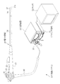
図1において、内視鏡システム2は、電子内視鏡10、プロセッサ装置11、光源装置12などから構成される。電子内視鏡10は、体腔内に挿入される可撓性の挿入部14と、挿入部14の基端部分に連設された操作部15と、プロセッサ装置11及び光源装置12に接続されるユニバーサルコード16とを備えている。
In FIG. 1, an endoscope system 2 includes an electronic endoscope 10, a
挿入部14の先端には、体腔内撮影用の固体撮像素子42(図3参照)などが内蔵された先端部17が連設されている。先端部17の後方には、複数の湾曲駒を連結した湾曲部18が設けられている。湾曲部18は、操作部15に設けられたアングルノブ19が操作されて、挿入部14内に挿設されたワイヤが押し引きされることにより、上下左右方向に湾曲動作する。これにより、先端部17が体腔内の所望の方向に向けられる。
At the distal end of the
ユニバーサルコード16の基端は、コネクタ20に連結されている。コネクタ20は、複合タイプのものであり、コネクタ20にはプロセッサ装置11が接続される他、光源装置12が接続される。
The base end of the
プロセッサ装置11は、ユニバーサルコード16内に挿通された信号線48(図3参照)を介して電子内視鏡10に給電を行い、固体撮像素子42の駆動を制御するとともに、固体撮像素子42からの出力信号を信号線48を介して受信し、受信した出力信号に各種信号処理を施して画像データに変換する。プロセッサ装置11で変換された画像データは、プロセッサ装置11にケーブル接続されたモニタ21に内視鏡画像として表示される。また、プロセッサ装置11は、コネクタ20を介して光源装置12と電気的に接続され、内視鏡システム2の動作を統括的に制御する。
The
図2において、先端部17の前面17aには、観察窓30、照明窓31、鉗子出口32、及び送気・送水用ノズル33が設けられている。観察窓30は、先端部17の片側中央に配置されている。照明窓31は、観察窓30に関して対称な位置に2個配され、体腔内の被観察部位に光源装置12からの照明光を照射する。鉗子出口32は、挿入部14内に配設された鉗子チャンネル50(図3参照)に接続され、操作部15に設けられた鉗子口22(図1参照)に連通している。鉗子口22には、注射針や高周波メスなどが先端に配された各種処置具が挿通され、各種処置具の先端が鉗子出口32から露呈される。送気・送水用ノズル33は、操作部15に設けられた送気・送水ボタン23(図1参照)の操作に応じて、光源装置12に内蔵された送気・送水装置から供給される洗浄水や空気を、観察窓30や体腔内に向けて噴射する。
In FIG. 2, an
図3において、観察窓30の奥には、体腔内の被観察部位の像光を取り込むための対物光学系40を保持する鏡筒41が配設されている。鏡筒41は、挿入部14の中心軸に対物光学系40の光軸が平行となるように取り付けられている。鏡筒41の後端には、対物光学系40を経由した被観察部位の像光を、略直角に曲げて固体撮像素子42に向けて導光するプリズム43が接続されている。
In FIG. 3, a
固体撮像素子42は、半導体チップからなるCCD(Charge Coupled Device)型イメージセンサであり、その表面には撮像面42aが表面に設けられている。固体撮像素子42は、撮像面42aがプリズム43の出射面と対向し、撮像面42aが対物光学系40の光軸と平行となるように配置されている。撮像面42a上には、四角枠状のスペーサ44を介して矩形板状のカバーガラス45が取り付けられている。固体撮像素子42、スペーサ44、及びカバーガラス45は、接着剤を介して組み付けられている。これにより、塵埃などの侵入から撮像面42aが保護されている。
The solid-
固体撮像素子42は、回路基板46に実装されている。回路基板46は、固体撮像素子42の下面、および側面を覆うように、固体撮像素子42を保持している。回路基板46には、固体撮像素子42の他、固体撮像素子42へ駆動信号を伝達するための配線(図示せず)などが実装されている。挿入部14の後端に向けて延設された回路基板46の後端部には、複数の入出力端子47が回路基板46の幅方向に並べて設けられている。入出力端子47には、ユニバーサルコード16を介してプロセッサ装置11との各種信号の遣り取りを媒介するための信号線48(図6に示す信号線48a〜48dからなる)が接合されており、入出力端子47は、回路基板46を介して固体撮像素子42と電気的に接続されている。信号線48は、可撓性の管状のケーブル49内にまとめて挿通されている。ケーブル49は、挿入部14、操作部15、及びユニバーサルコード16の各内部を挿通し、コネクタ20に接続されている。
The solid-
また、照明窓31の奥には、照明レンズ82(図6参照)が設けられている。照明レンズ82には、光源装置12からの照明光を導くライトガイド81(図6参照)の出射端が面している。ライトガイド81は、ケーブル49と同様に、挿入部14、操作部15、及びユニバーサルコード16の各内部を挿通し、コネクタ20に入射端が接続されている。光源装置12からライトガイド81によって照明レンズ82まで導かれた光は、照明窓31を通して体腔内へ照射される。
In addition, an illumination lens 82 (see FIG. 6) is provided in the back of the
図4において、固体撮像素子42は、インターライン転送方式のCCD型イメージセンサである。固体撮像素子42は、2次元マトリクス状に配置され、光電変換により入射光に応じた信号電荷を生成して蓄積する複数の受光素子(フォトダイオード)60と、受光素子60の垂直列ごとに設けられ、受光素子60から信号電荷を読み出し、読み出した信号電荷を垂直方向に転送する複数の垂直CCD61と、各垂直CCD61の出力端に共通に接続され、垂直CCD61から出力された信号電荷を水平方向に転送する水平CCD62と、水平CCD62の出力端に接続され、水平CCD62から出力された信号電荷を電圧に変換して外部に出力する出力部63とから構成されている。垂直CCD61は、4相CCDであり、位相が異なる4種の垂直CCD駆動パルスφV1〜φV4により駆動される。また、水平CCD62は、2相CCDであり、位相が異なる2種の水平CCD駆動パルスφH1,φH2により駆動される。
In FIG. 4, a solid-
出力部63は、水平CCD62の出力端から順に配設された出力ゲート64、フローティングディフュージョン(FD)部65、リセットゲート66、及びリセットドレイン67と、FD部65に入力端子が接続されたソースフォロア回路68とから構成されている。出力ゲート64には、所定のゲート電圧VOGが印加されており、水平CCD駆動パルスφH1,φH2に応じて水平CCD62の出力端から出力される信号電荷を、FD部65へ通過させる。
The output unit 63 includes an
FD部65は、出力ゲート64を介して水平CCD62から転送された信号電荷を蓄積し、信号電荷の蓄積電荷量に応じた電圧を生成する。ソースフォロア回路68は、FD部65での電荷電圧変換により生じた電圧を検出し、検出した電圧を緩衝増幅(インピーダンス変換)して出力する。リセットゲート66には、外部からリセットパルスφRGが印加され、水平CCD62からFD部65に次の画素の信号電荷が転送される前に、FD部65内に蓄積された電荷電圧変換後の信号電荷を、所定のリセットドレイン電圧VRDが印加されたリセットドレイン67へ破棄する。
The
ソースフォロア回路68から出力される出力信号Voutは、図5に示すように、1画素期間ごとに、出力ゲート64にリセットパルスφRGが印加された期間に対応するリセット部V1と、リセットパルスφRGの印加によりFD部65がリセットされた期間に対応するフィールドスルー部V2と、FD部65に信号電荷が蓄積された期間に対応する画素信号部V3とに分けられる。リセット部V1の電圧は、上記のリセットゲート66によるリセット動作に起因し、リセットパルスφRGの電圧、及びリセットゲート66とFD部65とのカップリング容量によって決定される。
As shown in FIG. 5, the output signal Vout output from the source follower circuit 68 includes, for each pixel period, a reset unit V1 corresponding to a period in which the reset pulse φRG is applied to the
なお、図示は省略するが、固体撮像素子42は、複数の色セグメントからなるカラーフィルタ(例えば、ベイヤー配列の原色カラーフィルタ)を備えた単板カラー撮像方式の固体撮像素子である。
Although not shown, the solid-
図6において、プロセッサ装置11は、CPU70、電源回路71、タイミングジェネレータ(TG)72、CCDドライバ73、相関二重サンプリング(CDS)回路74、アナログ/デジタル(A/D)変換器75、画像処理回路76、及びリセット部抽出回路(リセット部抽出手段)77から構成されている。プロセッサ装置11は、信号線48a〜48dを介して電子内視鏡10内の固体撮像素子42と電気的に接続されている。
In FIG. 6, a
CPU70は、プロセッサ装置11内の各部を制御するとともに、内視鏡システム2の全体を統括的に制御する。電源回路71は、電源電圧VDD及び接地電圧VSSを生成し、生成した電源電圧VDD及び接地電圧VSSを、プロセッサ装置11内の各部に供給するとともに、信号線48a,48bを介して固体撮像素子42に供給する。
The
TG72は、クロック信号を生成してCCDドライバ73に供給する。また、TG72は、相関二重サンプリング用のクランプパルス及びサンプルホールドパルスを生成してCDS回路74に供給するとともに、A/D変換用のクロック信号を生成してA/D変換器75に供給する。
The
CCDドライバ73は、TG72から入力されたクロック信号に基づき、前述の垂直CCD駆動パルスφV1〜φV4、水平CCD駆動パルスφH1,φH2、リセットパルスφRGなどの駆動信号を生成し、複数の信号線48cを介して、電子内視鏡10内の固体撮像素子42に伝送する。固体撮像素子42は、入力された駆動信号に従い、撮像動作を行う。なお、CCDドライバ73は、リセットパルスφRGを常に一定周期で固体撮像素子42に入力するため、固体撮像素子42の出力信号Voutには、画素信号部V3の有無に係わらず(つまり、暗時やブランキング期間においても)、常に一定周期でリセット部V1が現れる。
Based on the clock signal input from the
CDS回路74には、固体撮像素子42から出力された出力信号Voutが入力される。CDS回路74は、ノイズ除去回路であり、TG72から供給されるクランプパルスに基づいて、出力信号Voutのフィールドスルー部V2の電圧をクランプし、TG72から供給されるサンプルホールドパルスに基づいて出力信号Voutの画素信号部V3の電圧をサンプルホールドし、フィールドスルー部V2と画素信号部V3との差分値(電圧差)を信号として出力する。
The output signal Vout output from the solid-
A/D変換器75は、TG72から供給されるA/D変換用のクロック信号に基づいて、CDS回路74から出力された信号を量子化して、例えば8ビット(256階調)のデジタル信号に変換し、変換したデジタル信号を画像処理回路76に入力する。
The A /
画像処理回路76は、入力されたデジタル信号に対し、ホワイトバランス調整、ゲイン補正、色補間、輪郭強調、ガンマ補正、カラーマトリックス演算等の画像処理を行い、画像データを生成する。また、画像処理回路76は、画像データをモニタ21に表示するための信号形式に変換し、モニタ21に画像表示を行う。
The
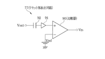
リセット部抽出回路77は、固体撮像素子42から出力された出力信号Voutに含まれるリセット部V1を抽出する。具体的には、リセット部抽出回路77は、図7に示すように、オペアンプからなる比較器90により構成されている。比較器90の「+」側入力端子には、バッファ91を介してコンデンサ92が接続されており、比較器90の「−」側入力端子には、基準電圧Vrefが印加されている。出力信号Voutは、直流バイアス成分を除去するコンデンサ92とバッファ91とを介して比較器90の「+」側入力端子に入力される。
The reset
比較器90は、入力された出力信号Voutを基準電圧Vrefと比較し、図8に示すように、基準電圧Vrefを下回る部分を接地電圧VSS、基準電圧Vrefを上回る部分を接地電圧VSSより大きい正電圧として出力する。なお、基準電圧Vrefは、フィールドスルー部V2の電圧より高く、リセット部V1の電圧より低い値に設定されている。これにより、比較器90の出力端子からは、リセット部V1のみからなるパルス波形状の抽出信号Vrsが出力され、出力された抽出信号Vrsは、CPU70に順次に入力される。
The comparator 90 compares the input output signal Vout with the reference voltage Vref, and as shown in FIG. 8, the portion below the reference voltage Vref is the ground voltage VSS and the portion above the reference voltage Vref is a positive voltage greater than the ground voltage VSS. Output as voltage. The reference voltage Vref is set to a value higher than the voltage of the field through portion V2 and lower than the voltage of the reset portion V1. As a result, a pulse wave-shaped extraction signal Vrs including only the reset unit V <b> 1 is output from the output terminal of the comparator 90, and the output extraction signal Vrs is sequentially input to the
CPU70は、リセット部抽出回路77から入力される抽出信号Vrsを監視し、固体撮像素子42とプロセッサ装置11とを接続する信号線48の接続状態を判定する接続状態判定手段としての機能を有する。上述したように、固体撮像素子42の出力信号Voutには、常に一定周期でリセット部V1が現れるため、リセット部V1の有無を検出することにより、信号線48の接続状態を判定することができる。
The
具体的には、CPU70は、TG72を作動させるとともに、接続状態の検出動作を開始し、リセット部抽出回路77から入力される抽出信号Vrsの立ち上がりエッジを検出することにより、抽出信号Vrs内に周期的に継続してリセット部V1が存在するか否かを判定する。CPU70は、図9に示すように、抽出信号Vrs内にリセット部V1が所定時間(少なくともリセットパルスφRGの1周期以上)現れないことを検出した場合には、信号線48の接続状態に異常が生じたと判定して、各部の動作を停止させる停止処理を行う。
Specifically, the
この停止処理では、CPU70は、TG72の動作を停止させることにより固体撮像素子42の撮像動作を停止させた後、電源回路71の動作を停止させ、さらに、光源装置12による光照射動作を停止させる。また、CPU70は、この停止処理とともに、画像処理回路76を介してモニタ21に、固体撮像素子42とプロセッサ装置11との接続状態に異常があることを知らせるメッセージを表示することにより、使用者に対してエラー報知を行う。
In this stop process, the
光源装置12は、キセノンランプやハロゲンランプなどの光源78と、光源78を駆動するための光源ドライバ79と、光源78から発せられた光を集光する集光レンズ80とを備えている。光源78から発せられた光は、集光レンズ80によって集光され、ライトガイド81の入射端に導かれ、上述のように電子内視鏡10の先端部17から体腔内へ照射される。光源ドライバ79は、CPU70からの制御に基づき、光源78の発光動作をオン/オフさせる。
The light source device 12 includes a light source 78 such as a xenon lamp or a halogen lamp, a
上記のように構成された内視鏡システム2で体腔内を観察する際には、電子内視鏡10、プロセッサ装置11、光源装置12、及びモニタ21の電源をオンにして、電子内視鏡10の挿入部14を体腔内に挿入し、光源装置12からの照明光で体腔内を照明しながら、固体撮像素子42により撮像される体腔内の画像をモニタ21で観察する。
When observing the inside of a body cavity with the endoscope system 2 configured as described above, the electronic endoscope 10, the
このとき、図10に示すフローチャートに沿った処理が行われる。まず、CPU70は、TG72を動作させ、CCDドライバ73により固体撮像素子42を駆動させる。固体撮像素子42からの出力信号Voutは、信号線48dを介してプロセッサ装置11内に伝送され、CDS回路74の他、リセット部抽出回路77に入力される。リセット部抽出回路77は、出力信号Voutに含まれるリセット部V1を抽出し、抽出信号VrsとしてCPU70に順次に入力する。CPU70は、抽出信号Vrs内のリセット部V1の有無を検出し、リセット部V1が所定時間現れない場合(つまり、リセット部抽出回路77により、リセット部V1が所定時間抽出されない場合)には、信号線48の接続状態が異常であると判定し、各部を制御して、固体撮像素子42の駆動を停止させるとともに、光源装置12による光照射動作を停止させる停止処理を行う。また、CPU70は、この停止処理と同時に、モニタ21にメッセージを表示させてエラー報知を行う。これにより、内視鏡システム2の使用者は、異常の発生を認識して、即座に体腔内の観察を中止することができる。
At this time, processing according to the flowchart shown in FIG. 10 is performed. First, the
以上説明したように、内視鏡システム2は、固体撮像素子42からプロセッサ装置11に伝送された出力信号Vout内のリセット部V1の有無に基づき、固体撮像素子42とプロセッサ装置11との間の接続状態を検出しているので、リセット部V1を消失させる原因となるものであれば、信号線48a〜48dのいずれに起因する異常であっても検出可能である。例えば、信号線48dの断線や他の信号線48a〜48c(例えば、接地電圧VSSが供給される信号線48b)との短絡の他、他の信号線48a〜48cの断線や短絡を検出することができる。このように、内視鏡システム2は、従来のように接続状態検出用の導体などを信号線48に沿って添設することなく、信号線48の接続状態を精度よく検出することができる。
As described above, the endoscope system 2 is based on the presence or absence of the reset unit V1 in the output signal Vout transmitted from the solid-
また、光源装置12には、通常、固体撮像素子42の受光光量に基づいて照明光の光量を制御する絞り機構(図示せず)が設けられており、信号線48が異常状態となり、固体撮像素子42からの出力信号が遮断された場合には、受光量が低下したと判断され、絞り機構は、照明光の光量を最大限とするように動作するが、上記のように光源装置12の停止処理を行うことにより、体腔内への不用な光照射を防止することができる。
In addition, the light source device 12 is usually provided with a diaphragm mechanism (not shown) that controls the amount of illumination light based on the amount of light received by the solid-
なお、上記実施形態では、リセット部抽出回路77をオペアンプからなる比較器90により構成しているが、本発明はこれに限定されず、リセット部抽出回路77は、出力信号Voutからリセット部V1を抽出することができるものであれば、ピークホールド回路やサンプルホールド回路などの検出回路により構成しても良い。この場合には、CPU70は、検出回路により検出された部分の電圧値が所定範囲内であるかを判定することにより、その検出部がリセット部V1であるか否かを判断すればよい。
In the above-described embodiment, the reset
また、上記実施形態では、CPU70は、抽出信号Vrsの立ち上がりエッジを検出することによりリセット部V1の有無を検出しているが、本発明はこれに限定されず、抽出信号Vrsの立ち上がりエッジ及び立ち下りエッジを検出し、立ち上がりエッジから立ち下りエッジまでの幅(パルス幅)を、リセット部V1の検出条件に含めることも好ましい。つまり、信号線48の異常等により生じたパルス状の波形をリセット部V1として誤検出しないようにすることで、リセット部V1の検出精度が向上し、その結果、信号線48の接続状態の検出精度がより向上する。
In the above embodiment, the
また、上記実施形態では、CPU70は、リセット部抽出回路77により、リセット部V1が継続して所定時間抽出されないことを条件として、信号線48の接続状態の判定を行っているが、本発明はこれに限定されず、さらに、リセット部V1が本来の周期とは異なる周期で抽出されること(つまり、リセット部V1の出現周波数の変化)を判定条件に加えることも好ましい。これにより、断線や短絡までに達しない程度の間断的な不具合(接触不良等)が信号線48に生じたことも検出することができる。
In the above-described embodiment, the
また、上記実施形態では、CPU70は、リセット部抽出回路77により、リセット部V1が継続して所定時間抽出されないことを条件にエラー報知を行っているが、本発明はこれに限定されず、さらに、図11に示すように、上記の所定時間が経過する前に事前警告を行うことも好ましい。この事前警告は、断線や短絡が生じる可能性があることを報知するものであり、上記のエラー報知と同様に、モニタ21にメッセージを表示させることにより行う。この事前警告により、使用者は、断線や短絡が生じる前に、観察の中止など、より迅速な対応を行うことができる。なお、この事前警告やエラー報知は、モニタ21によるメッセージ表示に限らず、音声出力などの他の報知方法により行っても良い。
In the above embodiment, the
また、上記実施形態では、出力信号Voutが入力されるリセット部抽出回路77及びCDS回路74をプロセッサ装置11内に設けているが、本発明はこれに限定されず、リセット部抽出回路77及びCDS回路74は、操作部15などの電子内視鏡10の内部に設けても良い。
In the above-described embodiment, the reset
また、上記実施形態では、撮像システムとして内視鏡システムを例示して説明したが、本発明はこれに限定されず、固体撮像素子と外部装置とが信号線を介して接続され、該信号線を介して固体撮像素子の出力信号を伝送するものであれば、電子内視鏡と超音波プローブを複合した超音波内視鏡システムや、撮像機能を備える鏡筒が本体に着脱可能なデジタルカメラ、カメラとパソコンとからなるWebカメラシステム等、いかなる撮像システムにも適用可能である。 In the above embodiment, the endoscope system is described as an example of the imaging system. However, the present invention is not limited to this, and the solid-state imaging device and an external device are connected via a signal line. If the output signal of the solid-state image sensor is transmitted via a digital endoscope, an ultrasonic endoscope system that combines an electronic endoscope and an ultrasonic probe, or a digital camera in which a lens barrel having an imaging function can be attached to and detached from the main body The present invention can be applied to any imaging system such as a Web camera system including a camera and a personal computer.
2 内視鏡システム
10 電子内視鏡
11 プロセッサ装置(外部装置)
12 光源装置
21 モニタ(エラー報知手段)
42 固体撮像素子
48 信号線
48a〜48d 信号線
65 FD部
66 リセットゲート
67 リセットドレイン
70 CPU(接続状態判定手段)
71 電源回路
73 CCDドライバ
77 リセット部抽出回路(リセット部抽出手段)
78 光源
79 光源ドライバ
90 比較器
2 Endoscope system 10
12
42 Solid-state image sensor 48 Signal line 48a-
71
78
Claims (7)
前記信号線から前記出力信号を受信し、前記出力信号から前記リセット動作に起因するリセット部を抽出するリセット部抽出手段と、
前記リセット部抽出手段により抽出される前記リセット部の有無に基づいて、前記信号線の接続状態が異常であるか否かを判定する接続状態判定手段と、
を備えたことを特徴とする撮像システム。 A solid-state imaging device that periodically performs a reset operation for discarding signal charges after charge-voltage conversion, and is connected to the solid-state imaging device by a signal line, and receives an output signal from the solid-state imaging device via the signal line In an imaging system comprising an external device that generates an image,
A reset unit extracting means for receiving the output signal from the signal line and extracting a reset unit resulting from the reset operation from the output signal;
A connection state determination unit that determines whether or not the connection state of the signal line is abnormal based on the presence or absence of the reset unit extracted by the reset unit extraction unit;
An imaging system comprising:
前記接続状態判定手段は、前記信号線の接続状態を異常と判定した場合に、前記電源供給及び駆動制御を停止させることを特徴とする請求項1または2に記載の撮像システム。 The solid-state imaging device is supplied with power and driven from the external device,
The imaging system according to claim 1, wherein the connection state determination unit stops the power supply and drive control when the connection state of the signal line is determined to be abnormal.
前記信号線から前記出力信号を受信し、前記出力信号から前記リセット動作に起因するリセット部を抽出するリセット部抽出手段と、
前記リセット部抽出手段により抽出される前記リセット部の有無に基づいて、前記信号線の接続状態が異常であるか否かを判定する接続状態判定手段と、
を備えたことを特徴とする内視鏡システム。 An endoscope having a built-in solid-state imaging device that periodically performs a reset operation for discarding signal charges after charge-voltage conversion, and connected to the solid-state imaging device by a signal line, and from the solid-state imaging device via the signal line In an endoscope system comprising an external device that receives an output signal and generates an image,
A reset unit extracting means for receiving the output signal from the signal line and extracting a reset unit resulting from the reset operation from the output signal;
A connection state determination unit that determines whether or not the connection state of the signal line is abnormal based on the presence or absence of the reset unit extracted by the reset unit extraction unit;
An endoscope system comprising:
Priority Applications (1)
| Application Number | Priority Date | Filing Date | Title |
|---|---|---|---|
| JP2008043826A JP2009201541A (en) | 2008-02-26 | 2008-02-26 | Imaging system and endoscopic system |
Applications Claiming Priority (1)
| Application Number | Priority Date | Filing Date | Title |
|---|---|---|---|
| JP2008043826A JP2009201541A (en) | 2008-02-26 | 2008-02-26 | Imaging system and endoscopic system |
Publications (1)
| Publication Number | Publication Date |
|---|---|
| JP2009201541A true JP2009201541A (en) | 2009-09-10 |
Family
ID=41144404
Family Applications (1)
| Application Number | Title | Priority Date | Filing Date |
|---|---|---|---|
| JP2008043826A Pending JP2009201541A (en) | 2008-02-26 | 2008-02-26 | Imaging system and endoscopic system |
Country Status (1)
| Country | Link |
|---|---|
| JP (1) | JP2009201541A (en) |
Cited By (2)
| Publication number | Priority date | Publication date | Assignee | Title |
|---|---|---|---|---|
| JP6219012B1 (en) * | 2016-08-02 | 2017-10-25 | オリンパス株式会社 | Endoscope system and signal processing apparatus |
| WO2018025430A1 (en) * | 2016-08-02 | 2018-02-08 | オリンパス株式会社 | Endoscope system and signal processing device |
-
2008
- 2008-02-26 JP JP2008043826A patent/JP2009201541A/en active Pending
Cited By (5)
| Publication number | Priority date | Publication date | Assignee | Title |
|---|---|---|---|---|
| JP6219012B1 (en) * | 2016-08-02 | 2017-10-25 | オリンパス株式会社 | Endoscope system and signal processing apparatus |
| WO2018025430A1 (en) * | 2016-08-02 | 2018-02-08 | オリンパス株式会社 | Endoscope system and signal processing device |
| CN109310281A (en) * | 2016-08-02 | 2019-02-05 | 奥林巴斯株式会社 | Endoscope system and signal processing device |
| US10750110B2 (en) | 2016-08-02 | 2020-08-18 | Olympus Corporation | Endoscope system and signal processor to determine a short or an open clock signal wire |
| CN109310281B (en) * | 2016-08-02 | 2021-03-12 | 奥林巴斯株式会社 | Endoscope system and signal processing device |
Similar Documents
| Publication | Publication Date | Title |
|---|---|---|
| US20090216080A1 (en) | Electronic communication system and endoscope system | |
| EP2742849B1 (en) | Endoscope apparatus and image pickup control method thereof | |
| JP6138406B1 (en) | Imaging device, endoscope and endoscope system | |
| JP2009201540A (en) | Imaging system and endoscope system | |
| JP5384409B2 (en) | Method of operating a CMOS image sensor in an endoscope apparatus | |
| EP3100667B1 (en) | Endoscope apparatus and image pickup control method thereof | |
| CN105075242B (en) | Photographing element, camera device, endoscope, the driving method of endoscopic system and photographing element | |
| US20120178992A1 (en) | Endoscopic image processing apparatus and endoscope system | |
| JP5132419B2 (en) | Endoscope system and option board | |
| JP5336410B2 (en) | Endoscope system and operating method thereof | |
| EP2743887B1 (en) | Endoscope apparatus and image processing method thereof | |
| JP2005305124A (en) | Electronic endoscope device | |
| JP6266091B2 (en) | Endoscopic imaging device | |
| JP5289371B2 (en) | Endoscope device and processor device in endoscope system | |
| JP2009195601A (en) | Imaging system and endoscope system | |
| JPWO2016129138A1 (en) | Image sensor | |
| JP2017200129A (en) | Imaging apparatus | |
| JP2009213629A (en) | Image pickup system and endoscope system | |
| WO2015015849A1 (en) | Imaging module, imaging unit, and endoscope device | |
| JP2009045366A (en) | Endoscope | |
| JP2017120972A (en) | Imaging device | |
| JP2010082224A (en) | Imaging apparatus |
Legal Events
| Date | Code | Title | Description |
|---|---|---|---|
| A711 | Notification of change in applicant |
Free format text: JAPANESE INTERMEDIATE CODE: A711 Effective date: 20100618 |