JP2009222902A - 電気泳動表示装置及び電子機器 - Google Patents
電気泳動表示装置及び電子機器 Download PDFInfo
- Publication number
- JP2009222902A JP2009222902A JP2008066227A JP2008066227A JP2009222902A JP 2009222902 A JP2009222902 A JP 2009222902A JP 2008066227 A JP2008066227 A JP 2008066227A JP 2008066227 A JP2008066227 A JP 2008066227A JP 2009222902 A JP2009222902 A JP 2009222902A
- Authority
- JP
- Japan
- Prior art keywords
- electrophoretic
- display device
- substrate
- pixel electrodes
- electrophoretic display
- Prior art date
- Legal status (The legal status is an assumption and is not a legal conclusion. Google has not performed a legal analysis and makes no representation as to the accuracy of the status listed.)
- Granted
Links
- 239000000758 substrate Substances 0.000 claims abstract description 70
- 239000010410 layer Substances 0.000 claims abstract description 25
- 239000012790 adhesive layer Substances 0.000 claims abstract description 16
- 238000004891 communication Methods 0.000 claims description 11
- 230000005684 electric field Effects 0.000 abstract description 21
- 239000002245 particle Substances 0.000 description 19
- 239000003094 microcapsule Substances 0.000 description 13
- 239000006059 cover glass Substances 0.000 description 8
- 239000000049 pigment Substances 0.000 description 6
- 239000002775 capsule Substances 0.000 description 5
- GWEVSGVZZGPLCZ-UHFFFAOYSA-N Titan oxide Chemical compound O=[Ti]=O GWEVSGVZZGPLCZ-UHFFFAOYSA-N 0.000 description 4
- 238000010586 diagram Methods 0.000 description 4
- 239000006185 dispersion Substances 0.000 description 4
- 239000002612 dispersion medium Substances 0.000 description 4
- 239000011521 glass Substances 0.000 description 4
- 239000007788 liquid Substances 0.000 description 4
- 239000000463 material Substances 0.000 description 4
- 229920000139 polyethylene terephthalate Polymers 0.000 description 4
- 239000005020 polyethylene terephthalate Substances 0.000 description 4
- 239000003566 sealing material Substances 0.000 description 4
- 210000000707 wrist Anatomy 0.000 description 4
- 239000000853 adhesive Substances 0.000 description 3
- 239000007822 coupling agent Substances 0.000 description 3
- 238000001962 electrophoresis Methods 0.000 description 3
- 238000007747 plating Methods 0.000 description 3
- 229920003229 poly(methyl methacrylate) Polymers 0.000 description 3
- -1 polyethylene terephthalate Polymers 0.000 description 3
- 239000004926 polymethyl methacrylate Substances 0.000 description 3
- 229920005989 resin Polymers 0.000 description 3
- 239000011347 resin Substances 0.000 description 3
- XLYOFNOQVPJJNP-UHFFFAOYSA-N water Substances O XLYOFNOQVPJJNP-UHFFFAOYSA-N 0.000 description 3
- PXHVJJICTQNCMI-UHFFFAOYSA-N Nickel Chemical compound [Ni] PXHVJJICTQNCMI-UHFFFAOYSA-N 0.000 description 2
- 229920012266 Poly(ether sulfone) PES Polymers 0.000 description 2
- XUIMIQQOPSSXEZ-UHFFFAOYSA-N Silicon Chemical compound [Si] XUIMIQQOPSSXEZ-UHFFFAOYSA-N 0.000 description 2
- 229920001807 Urea-formaldehyde Polymers 0.000 description 2
- 230000001070 adhesive effect Effects 0.000 description 2
- 239000001055 blue pigment Substances 0.000 description 2
- 239000006229 carbon black Substances 0.000 description 2
- 150000001875 compounds Chemical class 0.000 description 2
- 239000007791 liquid phase Substances 0.000 description 2
- 238000012423 maintenance Methods 0.000 description 2
- 238000004519 manufacturing process Methods 0.000 description 2
- 239000011159 matrix material Substances 0.000 description 2
- 229910052751 metal Inorganic materials 0.000 description 2
- 239000002184 metal Substances 0.000 description 2
- 239000003921 oil Substances 0.000 description 2
- 230000003287 optical effect Effects 0.000 description 2
- 230000002093 peripheral effect Effects 0.000 description 2
- IEQIEDJGQAUEQZ-UHFFFAOYSA-N phthalocyanine Chemical compound N1C(N=C2C3=CC=CC=C3C(N=C3C4=CC=CC=C4C(=N4)N3)=N2)=C(C=CC=C2)C2=C1N=C1C2=CC=CC=C2C4=N1 IEQIEDJGQAUEQZ-UHFFFAOYSA-N 0.000 description 2
- 239000004417 polycarbonate Substances 0.000 description 2
- 229920000515 polycarbonate Polymers 0.000 description 2
- 229910052710 silicon Inorganic materials 0.000 description 2
- 239000010703 silicon Substances 0.000 description 2
- 239000004094 surface-active agent Substances 0.000 description 2
- 239000004408 titanium dioxide Substances 0.000 description 2
- 238000002834 transmittance Methods 0.000 description 2
- 238000004804 winding Methods 0.000 description 2
- FWLHAQYOFMQTHQ-UHFFFAOYSA-N 2-N-[8-[[8-(4-aminoanilino)-10-phenylphenazin-10-ium-2-yl]amino]-10-phenylphenazin-10-ium-2-yl]-8-N,10-diphenylphenazin-10-ium-2,8-diamine hydroxy-oxido-dioxochromium Chemical compound O[Cr]([O-])(=O)=O.O[Cr]([O-])(=O)=O.O[Cr]([O-])(=O)=O.Nc1ccc(Nc2ccc3nc4ccc(Nc5ccc6nc7ccc(Nc8ccc9nc%10ccc(Nc%11ccccc%11)cc%10[n+](-c%10ccccc%10)c9c8)cc7[n+](-c7ccccc7)c6c5)cc4[n+](-c4ccccc4)c3c2)cc1 FWLHAQYOFMQTHQ-UHFFFAOYSA-N 0.000 description 1
- JBRZTFJDHDCESZ-UHFFFAOYSA-N AsGa Chemical compound [As]#[Ga] JBRZTFJDHDCESZ-UHFFFAOYSA-N 0.000 description 1
- RYGMFSIKBFXOCR-UHFFFAOYSA-N Copper Chemical compound [Cu] RYGMFSIKBFXOCR-UHFFFAOYSA-N 0.000 description 1
- 239000004593 Epoxy Substances 0.000 description 1
- 229910001218 Gallium arsenide Inorganic materials 0.000 description 1
- 108010010803 Gelatin Proteins 0.000 description 1
- 229920000084 Gum arabic Polymers 0.000 description 1
- 229920000106 Liquid crystal polymer Polymers 0.000 description 1
- 239000004977 Liquid-crystal polymers (LCPs) Substances 0.000 description 1
- 239000004642 Polyimide Substances 0.000 description 1
- NRCMAYZCPIVABH-UHFFFAOYSA-N Quinacridone Chemical compound N1C2=CC=CC=C2C(=O)C2=C1C=C1C(=O)C3=CC=CC=C3NC1=C2 NRCMAYZCPIVABH-UHFFFAOYSA-N 0.000 description 1
- 241000978776 Senegalia senegal Species 0.000 description 1
- RTAQQCXQSZGOHL-UHFFFAOYSA-N Titanium Chemical compound [Ti] RTAQQCXQSZGOHL-UHFFFAOYSA-N 0.000 description 1
- 235000010489 acacia gum Nutrition 0.000 description 1
- 239000000205 acacia gum Substances 0.000 description 1
- NIXOWILDQLNWCW-UHFFFAOYSA-N acrylic acid group Chemical group C(C=C)(=O)O NIXOWILDQLNWCW-UHFFFAOYSA-N 0.000 description 1
- 230000002411 adverse Effects 0.000 description 1
- 239000005456 alcohol based solvent Substances 0.000 description 1
- 150000001338 aliphatic hydrocarbons Chemical class 0.000 description 1
- 229910052782 aluminium Inorganic materials 0.000 description 1
- XAGFODPZIPBFFR-UHFFFAOYSA-N aluminium Chemical compound [Al] XAGFODPZIPBFFR-UHFFFAOYSA-N 0.000 description 1
- 150000004945 aromatic hydrocarbons Chemical class 0.000 description 1
- 125000003118 aryl group Chemical group 0.000 description 1
- 230000015572 biosynthetic process Effects 0.000 description 1
- 150000007942 carboxylates Chemical class 0.000 description 1
- 239000003795 chemical substances by application Substances 0.000 description 1
- 239000000084 colloidal system Substances 0.000 description 1
- 239000002131 composite material Substances 0.000 description 1
- 239000004020 conductor Substances 0.000 description 1
- 229910052802 copper Inorganic materials 0.000 description 1
- 239000010949 copper Substances 0.000 description 1
- 230000007547 defect Effects 0.000 description 1
- 230000002542 deteriorative effect Effects 0.000 description 1
- 239000002270 dispersing agent Substances 0.000 description 1
- 229920001971 elastomer Polymers 0.000 description 1
- 239000003792 electrolyte Substances 0.000 description 1
- 238000005516 engineering process Methods 0.000 description 1
- 239000003822 epoxy resin Substances 0.000 description 1
- 150000002148 esters Chemical class 0.000 description 1
- 229920000159 gelatin Polymers 0.000 description 1
- 239000008273 gelatin Substances 0.000 description 1
- 235000019322 gelatine Nutrition 0.000 description 1
- 235000011852 gelatine desserts Nutrition 0.000 description 1
- PCHJSUWPFVWCPO-UHFFFAOYSA-N gold Chemical compound [Au] PCHJSUWPFVWCPO-UHFFFAOYSA-N 0.000 description 1
- 229910052737 gold Inorganic materials 0.000 description 1
- 239000010931 gold Substances 0.000 description 1
- 239000001056 green pigment Substances 0.000 description 1
- 150000008282 halocarbons Chemical class 0.000 description 1
- 229930195733 hydrocarbon Natural products 0.000 description 1
- AMGQUBHHOARCQH-UHFFFAOYSA-N indium;oxotin Chemical compound [In].[Sn]=O AMGQUBHHOARCQH-UHFFFAOYSA-N 0.000 description 1
- 230000008595 infiltration Effects 0.000 description 1
- 238000001764 infiltration Methods 0.000 description 1
- 239000010954 inorganic particle Substances 0.000 description 1
- 238000009413 insulation Methods 0.000 description 1
- PXZQEOJJUGGUIB-UHFFFAOYSA-N isoindolin-1-one Chemical compound C1=CC=C2C(=O)NCC2=C1 PXZQEOJJUGGUIB-UHFFFAOYSA-N 0.000 description 1
- 150000002576 ketones Chemical class 0.000 description 1
- 239000005355 lead glass Substances 0.000 description 1
- 239000000314 lubricant Substances 0.000 description 1
- 238000000034 method Methods 0.000 description 1
- 239000000203 mixture Substances 0.000 description 1
- 238000012986 modification Methods 0.000 description 1
- 230000004048 modification Effects 0.000 description 1
- 229910052759 nickel Inorganic materials 0.000 description 1
- 239000011146 organic particle Substances 0.000 description 1
- 239000004033 plastic Substances 0.000 description 1
- 229920003023 plastic Polymers 0.000 description 1
- 229920000767 polyaniline Polymers 0.000 description 1
- 229920000647 polyepoxide Polymers 0.000 description 1
- 229920000728 polyester Polymers 0.000 description 1
- 239000011112 polyethylene naphthalate Substances 0.000 description 1
- 229920001721 polyimide Polymers 0.000 description 1
- 229920000642 polymer Polymers 0.000 description 1
- 230000001681 protective effect Effects 0.000 description 1
- 239000010453 quartz Substances 0.000 description 1
- 239000001054 red pigment Substances 0.000 description 1
- 239000005060 rubber Substances 0.000 description 1
- 229910052594 sapphire Inorganic materials 0.000 description 1
- 239000010980 sapphire Substances 0.000 description 1
- 150000004756 silanes Chemical class 0.000 description 1
- VYPSYNLAJGMNEJ-UHFFFAOYSA-N silicon dioxide Inorganic materials O=[Si]=O VYPSYNLAJGMNEJ-UHFFFAOYSA-N 0.000 description 1
- 239000000344 soap Substances 0.000 description 1
- 239000003381 stabilizer Substances 0.000 description 1
- 229920002803 thermoplastic polyurethane Polymers 0.000 description 1
- 229920001187 thermosetting polymer Polymers 0.000 description 1
- 239000010936 titanium Substances 0.000 description 1
- 229910052719 titanium Inorganic materials 0.000 description 1
- 239000002966 varnish Substances 0.000 description 1
- 239000012463 white pigment Substances 0.000 description 1
- 239000001052 yellow pigment Substances 0.000 description 1
Images



Classifications
-
- G—PHYSICS
- G02—OPTICS
- G02F—OPTICAL DEVICES OR ARRANGEMENTS FOR THE CONTROL OF LIGHT BY MODIFICATION OF THE OPTICAL PROPERTIES OF THE MEDIA OF THE ELEMENTS INVOLVED THEREIN; NON-LINEAR OPTICS; FREQUENCY-CHANGING OF LIGHT; OPTICAL LOGIC ELEMENTS; OPTICAL ANALOGUE/DIGITAL CONVERTERS
- G02F1/00—Devices or arrangements for the control of the intensity, colour, phase, polarisation or direction of light arriving from an independent light source, e.g. switching, gating or modulating; Non-linear optics
- G02F1/01—Devices or arrangements for the control of the intensity, colour, phase, polarisation or direction of light arriving from an independent light source, e.g. switching, gating or modulating; Non-linear optics for the control of the intensity, phase, polarisation or colour
- G02F1/165—Devices or arrangements for the control of the intensity, colour, phase, polarisation or direction of light arriving from an independent light source, e.g. switching, gating or modulating; Non-linear optics for the control of the intensity, phase, polarisation or colour based on translational movement of particles in a fluid under the influence of an applied field
- G02F1/166—Devices or arrangements for the control of the intensity, colour, phase, polarisation or direction of light arriving from an independent light source, e.g. switching, gating or modulating; Non-linear optics for the control of the intensity, phase, polarisation or colour based on translational movement of particles in a fluid under the influence of an applied field characterised by the electro-optical or magneto-optical effect
- G02F1/167—Devices or arrangements for the control of the intensity, colour, phase, polarisation or direction of light arriving from an independent light source, e.g. switching, gating or modulating; Non-linear optics for the control of the intensity, phase, polarisation or colour based on translational movement of particles in a fluid under the influence of an applied field characterised by the electro-optical or magneto-optical effect by electrophoresis
-
- G—PHYSICS
- G02—OPTICS
- G02F—OPTICAL DEVICES OR ARRANGEMENTS FOR THE CONTROL OF LIGHT BY MODIFICATION OF THE OPTICAL PROPERTIES OF THE MEDIA OF THE ELEMENTS INVOLVED THEREIN; NON-LINEAR OPTICS; FREQUENCY-CHANGING OF LIGHT; OPTICAL LOGIC ELEMENTS; OPTICAL ANALOGUE/DIGITAL CONVERTERS
- G02F1/00—Devices or arrangements for the control of the intensity, colour, phase, polarisation or direction of light arriving from an independent light source, e.g. switching, gating or modulating; Non-linear optics
- G02F1/01—Devices or arrangements for the control of the intensity, colour, phase, polarisation or direction of light arriving from an independent light source, e.g. switching, gating or modulating; Non-linear optics for the control of the intensity, phase, polarisation or colour
- G02F1/13—Devices or arrangements for the control of the intensity, colour, phase, polarisation or direction of light arriving from an independent light source, e.g. switching, gating or modulating; Non-linear optics for the control of the intensity, phase, polarisation or colour based on liquid crystals, e.g. single liquid crystal display cells
- G02F1/133—Constructional arrangements; Operation of liquid crystal cells; Circuit arrangements
- G02F1/1333—Constructional arrangements; Manufacturing methods
- G02F1/1343—Electrodes
- G02F1/134309—Electrodes characterised by their geometrical arrangement
- G02F1/134327—Segmented, e.g. alpha numeric display
-
- G—PHYSICS
- G02—OPTICS
- G02F—OPTICAL DEVICES OR ARRANGEMENTS FOR THE CONTROL OF LIGHT BY MODIFICATION OF THE OPTICAL PROPERTIES OF THE MEDIA OF THE ELEMENTS INVOLVED THEREIN; NON-LINEAR OPTICS; FREQUENCY-CHANGING OF LIGHT; OPTICAL LOGIC ELEMENTS; OPTICAL ANALOGUE/DIGITAL CONVERTERS
- G02F1/00—Devices or arrangements for the control of the intensity, colour, phase, polarisation or direction of light arriving from an independent light source, e.g. switching, gating or modulating; Non-linear optics
- G02F1/01—Devices or arrangements for the control of the intensity, colour, phase, polarisation or direction of light arriving from an independent light source, e.g. switching, gating or modulating; Non-linear optics for the control of the intensity, phase, polarisation or colour
- G02F1/13—Devices or arrangements for the control of the intensity, colour, phase, polarisation or direction of light arriving from an independent light source, e.g. switching, gating or modulating; Non-linear optics for the control of the intensity, phase, polarisation or colour based on liquid crystals, e.g. single liquid crystal display cells
- G02F1/133—Constructional arrangements; Operation of liquid crystal cells; Circuit arrangements
- G02F1/136—Liquid crystal cells structurally associated with a semi-conducting layer or substrate, e.g. cells forming part of an integrated circuit
- G02F1/1362—Active matrix addressed cells
- G02F1/136227—Through-hole connection of the pixel electrode to the active element through an insulation layer
-
- G—PHYSICS
- G02—OPTICS
- G02F—OPTICAL DEVICES OR ARRANGEMENTS FOR THE CONTROL OF LIGHT BY MODIFICATION OF THE OPTICAL PROPERTIES OF THE MEDIA OF THE ELEMENTS INVOLVED THEREIN; NON-LINEAR OPTICS; FREQUENCY-CHANGING OF LIGHT; OPTICAL LOGIC ELEMENTS; OPTICAL ANALOGUE/DIGITAL CONVERTERS
- G02F1/00—Devices or arrangements for the control of the intensity, colour, phase, polarisation or direction of light arriving from an independent light source, e.g. switching, gating or modulating; Non-linear optics
- G02F1/01—Devices or arrangements for the control of the intensity, colour, phase, polarisation or direction of light arriving from an independent light source, e.g. switching, gating or modulating; Non-linear optics for the control of the intensity, phase, polarisation or colour
- G02F1/165—Devices or arrangements for the control of the intensity, colour, phase, polarisation or direction of light arriving from an independent light source, e.g. switching, gating or modulating; Non-linear optics for the control of the intensity, phase, polarisation or colour based on translational movement of particles in a fluid under the influence of an applied field
- G02F1/1675—Constructional details
- G02F1/1676—Electrodes
-
- G—PHYSICS
- G02—OPTICS
- G02F—OPTICAL DEVICES OR ARRANGEMENTS FOR THE CONTROL OF LIGHT BY MODIFICATION OF THE OPTICAL PROPERTIES OF THE MEDIA OF THE ELEMENTS INVOLVED THEREIN; NON-LINEAR OPTICS; FREQUENCY-CHANGING OF LIGHT; OPTICAL LOGIC ELEMENTS; OPTICAL ANALOGUE/DIGITAL CONVERTERS
- G02F2202/00—Materials and properties
- G02F2202/28—Adhesive materials or arrangements
Landscapes
- Physics & Mathematics (AREA)
- Nonlinear Science (AREA)
- General Physics & Mathematics (AREA)
- Optics & Photonics (AREA)
- Chemical & Material Sciences (AREA)
- Electrochemistry (AREA)
- Life Sciences & Earth Sciences (AREA)
- Chemical Kinetics & Catalysis (AREA)
- Health & Medical Sciences (AREA)
- Molecular Biology (AREA)
- Mathematical Physics (AREA)
- Crystallography & Structural Chemistry (AREA)
- Geometry (AREA)
- Engineering & Computer Science (AREA)
- Microelectronics & Electronic Packaging (AREA)
- Electrochromic Elements, Electrophoresis, Or Variable Reflection Or Absorption Elements (AREA)
Abstract
【解決手段】表示領域に複数の画素電極を有する第1基板と、第2基板上に共通電極、電気泳動層及び接着層が積層されてなり前記接着層を介して前記第1基板の前記表示領域に貼り合わされた電気泳動シートと、を備えた電気泳動表示装置であって、複数の前記画素電極のうち隣接する画素電極間の距離が5μm以上である。隣接する画素電極が互いの漏れ電界の影響を受けにくくなるため、クロストークの影響を緩和することができる。これにより、表示品質を維持することが可能となる。
【選択図】図3
Description
本発明では、複数の画素電極のうち隣接する画素電極間の距離が100μm以下であることとしたので、クロストークの影響を緩和しつつ高精度の表示を行うことが可能となる。
本発明によれば、第1基板に複数の画素電極のそれぞれに対応するスイッチング素子が設けられた、いわゆるアクティブ型の構成において、クロストークの影響を緩和し表示品質を維持することが可能となる。
本発明によれば、複数の画素電極が所定パターンに配列された複数のセグメント電極である、いわゆるセグメント型の構成において、クロストークの影響を緩和し表示品質を維持することが可能となる。
本発明によれば、複数のセグメント電極のそれぞれに平面視で重なる位置に第1基板及びセグメント電極を貫通して設けられた貫通孔と、当該貫通孔の内面を覆うように当該内面に沿って設けられ、一方の端部がセグメント電極に接続されると共に他方の端部が第1基板のうち画素電極の形成された面とは反対側の面に接続され、平面視中央部に一方の端部と他方の端部とを連通する連通孔を有する接続部と、を有し、この連通孔の径が100μm以下になっていることとしたので、連通孔の設けられた領域が非表示領域となるのを回避することができる。セグメント型の構成において表示品質が低下するのを一層確実に回避することができ、表示品質の維持に資することになる。
本発明によれば、表示品質を維持することが可能な電気泳動表示装置が搭載されているので、表示部の表示特性が高い電子機器を得ることができる。
以下、図面を参照して本発明の第1実施形態を説明する。本実施形態では、アクティブマトリクス型の電気泳動表示装置を例に挙げて説明する。なお、以下の説明に用いた各図においては、各層や各部材を図面上で認識可能な程度の大きさとするため、各層や各部材毎に縮尺を異ならせてある。
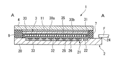
透明基板30は電気泳動層31を保持する基板であり、例えばポリエチレンテレフタレート(PET)、ポリエーテルスルホン(PES)、ポリカーボネイト(PC)など光透過性の高い材料からなる矩形の基板である。透明基板30の表面30a側は電気泳動表示装置1の表示面側になっている。
マイクロカプセル32は電気泳動分散液が封入された略球状のカプセルであり、各カプセルの直径はほぼ同一(40μm〜50μm)になっている。マイクロカプセル32のカプセル壁膜を形成する材料としては、アラビアガム・ゼラチンの複合膜、ウレタン樹脂、ウレア樹脂、尿素樹脂などの化合物が挙げられる。マイクロカプセル32に封入された電気泳動分散液は、複数の電気泳動粒子と、当該電気泳動粒子を分散させるための液層分散媒とからなる。
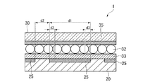
同図に示すように、各画素電極25の図中左右方向の寸法d1は80μm程度になっており、このような画素電極25が距離d2をおいて配列されている。当該距離d2については、5μm以上100μm以下であることが好ましく、本実施形態では8μmになっている。当該距離d2を5μm以上とすることで、隣接する画素電極25の電界の影響を受ける部分d3の範囲が大きくなりすぎるのを回避し、表示特性の悪化を防ぐことができるようになっている。また、当該距離d2を100μm以下とすることで、非表示領域が広くなりすぎるのを回避し、表示精度の維持を図っている。距離d2を8μmとした場合、隣接画素電極25からの電界の影響を受ける部分d3は10μm程度となり、有効な画素領域(d1−2d3)を十分に確保できることから、表示への影響がほとんど気にならなくなる。
画素電極25と共通電極35との間に共通電極35の電圧が画素電極25に対して相対的に高くなるように電圧を印加すると、正に帯電された黒色の電気泳動粒子はクーロン力によってマイクロカプセル32内のうち画素電極25側に引き寄せられる。一方、負に帯電された白色の電気泳動粒子はクーロン力によってマイクロカプセル32内の共通電極35側に引き寄せられる。この結果、マイクロカプセル32内の透明基板30側には白色の電気泳動粒子が集まることになり、電気泳動表示装置1の表示領域5にはこの白色の電気泳動粒子の色(白色)が表示されることとなる。
以下、本発明の第2実施形態を説明する。本実施形態では、セグメント型の電気泳動表示装置を例に挙げて説明する。
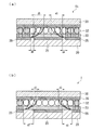
図5は本発明の電気泳動表示装置101の一実施形態を示す図であり、図6は図5に示す電気泳動表示装置101のB−B断面に沿った断面図であり、第1実施形態における図3に対応している。なお、以下の説明に用いた各図においては、各層や各部材を図面上で認識可能な程度の大きさとするため、各層や各部材毎に縮尺を異ならせてある。
次に、上記実施形態の電気泳動表示装置1、101を、電子機器に適用した場合について説明する。
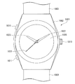
図7は、腕時計1000の正面図である。腕時計1000は、時計ケース1002と、時計ケース1002に連結された一対のバンド1003とを備えている。
例えば、
Claims (6)
- 表示領域に複数の画素電極を有する第1基板と、第2基板上に共通電極、電気泳動層及び接着層が積層されてなり前記接着層を介して前記第1基板の前記表示領域に貼り合わされた電気泳動シートと、を備えた電気泳動表示装置であって、
複数の前記画素電極のうち隣接する画素電極間の距離が5μm以上である
ことを特徴とする電気泳動表示装置。 - 複数の前記画素電極のうち隣接する画素電極間の距離が100μm以下である
ことを特徴とする請求項1に記載の電気泳動表示装置。 - 前記第1基板には、複数の前記画素電極のそれぞれに対応するスイッチング素子が設けられている
ことを特徴とする請求項1又は請求項2に記載の電気泳動表示装置。 - 複数の前記画素電極は、所定パターンに配列された複数のセグメント電極である
ことを特徴とする請求項1又は請求項2に記載の電気泳動表示装置。 - 複数の前記セグメント電極のそれぞれに平面視で重なる位置に、前記第1基板及び前記セグメント電極を貫通して設けられた貫通孔と、
前記貫通孔の内面を覆うように当該内面に沿って設けられ、一方の端部がセグメント電極に接続されると共に他方の端部が前記第1基板のうち前記画素電極の形成された面とは反対側の面に接続され、平面視中央部に前記一方の端部と前記他方の端部とを連通する連通孔を有する接続部と、
を有し、
前記連通孔の径が、100μm以下になっている
ことを特徴とする請求項4に記載の電気泳動表示装置。 - 請求項1から請求項5のうちいずれか一項に記載の電気泳動表示装置を搭載したことを特徴とする電子機器。
Priority Applications (4)
| Application Number | Priority Date | Filing Date | Title |
|---|---|---|---|
| JP2008066227A JP5266815B2 (ja) | 2008-03-14 | 2008-03-14 | 電気泳動表示装置及び電子機器 |
| US12/389,591 US7729040B2 (en) | 2008-03-14 | 2009-02-20 | Electrophoretic display device and electronic apparatus |
| CN2009100045340A CN101533197B (zh) | 2008-03-14 | 2009-03-06 | 电泳显示装置及电子设备 |
| KR1020090021607A KR101512857B1 (ko) | 2008-03-14 | 2009-03-13 | 전기 영동 표시 장치 및 전자 기기 |
Applications Claiming Priority (1)
| Application Number | Priority Date | Filing Date | Title |
|---|---|---|---|
| JP2008066227A JP5266815B2 (ja) | 2008-03-14 | 2008-03-14 | 電気泳動表示装置及び電子機器 |
Publications (2)
| Publication Number | Publication Date |
|---|---|
| JP2009222902A true JP2009222902A (ja) | 2009-10-01 |
| JP5266815B2 JP5266815B2 (ja) | 2013-08-21 |
Family
ID=41062735
Family Applications (1)
| Application Number | Title | Priority Date | Filing Date |
|---|---|---|---|
| JP2008066227A Expired - Fee Related JP5266815B2 (ja) | 2008-03-14 | 2008-03-14 | 電気泳動表示装置及び電子機器 |
Country Status (4)
| Country | Link |
|---|---|
| US (1) | US7729040B2 (ja) |
| JP (1) | JP5266815B2 (ja) |
| KR (1) | KR101512857B1 (ja) |
| CN (1) | CN101533197B (ja) |
Cited By (9)
| Publication number | Priority date | Publication date | Assignee | Title |
|---|---|---|---|---|
| JP2012027456A (ja) * | 2010-06-25 | 2012-02-09 | Semiconductor Energy Lab Co Ltd | 表示装置 |
| JP2012208416A (ja) * | 2011-03-30 | 2012-10-25 | Toppan Printing Co Ltd | 薄膜トランジスタアレイ、表示装置、およびそれらの製造方法 |
| US8331016B2 (en) | 2010-06-15 | 2012-12-11 | Seiko Epson Corporation | Electrophoretic display device |
| US8345347B2 (en) | 2010-04-20 | 2013-01-01 | Seiko Epson Corporation | Electrophoretic display device and electronic device |
| US8815330B2 (en) | 2010-04-14 | 2014-08-26 | Seiko Epson Corporation | Method for manufacturing electrophoretic display apparatus |
| KR20220001784A (ko) * | 2020-06-30 | 2022-01-06 | 엘지이노텍 주식회사 | 광 경로 제어 부재 및 이를 포함하는 디스플레이 장치 |
| KR20220001778A (ko) * | 2020-06-30 | 2022-01-06 | 엘지이노텍 주식회사 | 광 경로 제어 부재 및 이를 포함하는 디스플레이 장치 |
| KR20220032758A (ko) * | 2020-09-08 | 2022-03-15 | 엘지이노텍 주식회사 | 광 경로 제어 부재 및 이를 포함하는 디스플레이 장치 |
| WO2022075017A1 (ja) * | 2020-10-05 | 2022-04-14 | ソニーグループ株式会社 | 調光装置、画像表示装置及び表示装置 |
Families Citing this family (13)
| Publication number | Priority date | Publication date | Assignee | Title |
|---|---|---|---|---|
| TWI387943B (zh) * | 2009-03-30 | 2013-03-01 | Prime View Int Co Ltd | 電子紙顯示裝置 |
| TWI407227B (zh) * | 2009-10-01 | 2013-09-01 | Au Optronics Corp | 具控制電路保護功能之平面顯示裝置 |
| TWI387833B (zh) | 2009-12-01 | 2013-03-01 | Prime View Int Co Ltd | 電泳顯示器及其製造方法 |
| CN102109727B (zh) * | 2009-12-28 | 2013-06-19 | 元太科技工业股份有限公司 | 电泳显示器及其制造方法 |
| KR101148467B1 (ko) * | 2010-01-06 | 2012-05-25 | 삼성전기주식회사 | 전자종이 표시장치 |
| KR102160694B1 (ko) * | 2013-11-01 | 2020-09-29 | 삼성디스플레이 주식회사 | 표시 장치 및 그 제조 방법 |
| US9785032B2 (en) | 2013-11-12 | 2017-10-10 | E Ink Holdings Inc. | Active device array substrate and display panel |
| JP2016191848A (ja) * | 2015-03-31 | 2016-11-10 | セイコーエプソン株式会社 | 電気光学表示装置、電子機器、及び駆動方法 |
| KR102577801B1 (ko) * | 2016-04-05 | 2023-09-13 | 주식회사 나노브릭 | 전기 영동 디스플레이 장치 및 이의 제조 방법 |
| KR102812628B1 (ko) | 2020-04-17 | 2025-05-27 | 주식회사 솔루엠 | 디스플레이 장치 |
| WO2022025560A1 (ko) | 2020-07-28 | 2022-02-03 | 엘지이노텍 주식회사 | 광 경로 제어 부재 및 이를 포함하는 디스플레이 장치 |
| EP4209834B1 (en) | 2020-09-03 | 2026-03-11 | LG Innotek Co., Ltd. | Light path control member and display device comprising same |
| KR102416543B1 (ko) * | 2020-11-20 | 2022-07-05 | 엘지이노텍 주식회사 | 광 경로 제어 부재 및 이를 포함하는 디스플레이 장치 |
Citations (5)
| Publication number | Priority date | Publication date | Assignee | Title |
|---|---|---|---|---|
| JPH05232463A (ja) * | 1992-02-21 | 1993-09-10 | Matsushita Electric Works Ltd | 液晶素子 |
| JP2002040458A (ja) * | 2000-07-31 | 2002-02-06 | Seiko Epson Corp | 液晶装置および電子機器 |
| JP2006227470A (ja) * | 2005-02-21 | 2006-08-31 | Seiko Epson Corp | 電気光学装置および電子機器 |
| JP2007057585A (ja) * | 2005-08-22 | 2007-03-08 | Seiko Epson Corp | 電気泳動装置、電子機器 |
| JP2008052252A (ja) * | 2006-07-28 | 2008-03-06 | Seiko Epson Corp | 電気泳動表示パネルの駆動方法並びに駆動装置、電気泳動表示装置、および電子機器 |
Family Cites Families (9)
| Publication number | Priority date | Publication date | Assignee | Title |
|---|---|---|---|---|
| JP2003186065A (ja) | 2001-12-21 | 2003-07-03 | Canon Inc | 電気泳動表示装置及びその駆動方法 |
| TWI223729B (en) * | 2002-04-23 | 2004-11-11 | Sipix Imaging Inc | Improved segment electrophoretic displays and methods for their manufacture |
| JP4631294B2 (ja) | 2004-02-27 | 2011-02-16 | 富士ゼロックス株式会社 | 画像表示装置 |
| JP4609051B2 (ja) | 2004-11-29 | 2011-01-12 | Jsr株式会社 | 衝撃吸収積層構造体、lcd、プラズマディスプレイ、有機elディスプレイ、フィールドエミッションディスプレイ又は電子ペーパー用衝撃吸収積層構造体、及びディスプレイ装置 |
| US7304780B2 (en) * | 2004-12-17 | 2007-12-04 | Sipix Imaging, Inc. | Backplane design for display panels and processes for their manufacture |
| JP4718859B2 (ja) * | 2005-02-17 | 2011-07-06 | セイコーエプソン株式会社 | 電気泳動装置とその駆動方法、及び電子機器 |
| CN100456118C (zh) * | 2005-03-29 | 2009-01-28 | 精工爱普生株式会社 | 电泳显示装置 |
| JP4867247B2 (ja) * | 2005-09-14 | 2012-02-01 | セイコーエプソン株式会社 | 表示装置、駆動装置及び駆動方法 |
| KR101415569B1 (ko) * | 2007-05-14 | 2014-07-04 | 삼성디스플레이 주식회사 | 전기영동 유닛, 이를 구비한 표시 장치 및 그 제조 방법 |
-
2008
- 2008-03-14 JP JP2008066227A patent/JP5266815B2/ja not_active Expired - Fee Related
-
2009
- 2009-02-20 US US12/389,591 patent/US7729040B2/en not_active Expired - Fee Related
- 2009-03-06 CN CN2009100045340A patent/CN101533197B/zh not_active Expired - Fee Related
- 2009-03-13 KR KR1020090021607A patent/KR101512857B1/ko not_active Expired - Fee Related
Patent Citations (5)
| Publication number | Priority date | Publication date | Assignee | Title |
|---|---|---|---|---|
| JPH05232463A (ja) * | 1992-02-21 | 1993-09-10 | Matsushita Electric Works Ltd | 液晶素子 |
| JP2002040458A (ja) * | 2000-07-31 | 2002-02-06 | Seiko Epson Corp | 液晶装置および電子機器 |
| JP2006227470A (ja) * | 2005-02-21 | 2006-08-31 | Seiko Epson Corp | 電気光学装置および電子機器 |
| JP2007057585A (ja) * | 2005-08-22 | 2007-03-08 | Seiko Epson Corp | 電気泳動装置、電子機器 |
| JP2008052252A (ja) * | 2006-07-28 | 2008-03-06 | Seiko Epson Corp | 電気泳動表示パネルの駆動方法並びに駆動装置、電気泳動表示装置、および電子機器 |
Cited By (20)
| Publication number | Priority date | Publication date | Assignee | Title |
|---|---|---|---|---|
| US8815330B2 (en) | 2010-04-14 | 2014-08-26 | Seiko Epson Corporation | Method for manufacturing electrophoretic display apparatus |
| US8345347B2 (en) | 2010-04-20 | 2013-01-01 | Seiko Epson Corporation | Electrophoretic display device and electronic device |
| US8331016B2 (en) | 2010-06-15 | 2012-12-11 | Seiko Epson Corporation | Electrophoretic display device |
| JP2012027456A (ja) * | 2010-06-25 | 2012-02-09 | Semiconductor Energy Lab Co Ltd | 表示装置 |
| US9268193B2 (en) | 2010-06-25 | 2016-02-23 | Semiconductor Energy Laboratory Co., Ltd. | Display device |
| US9488895B2 (en) | 2010-06-25 | 2016-11-08 | Semiconductor Energy Laboratory Co., Ltd. | Display device |
| US9857658B2 (en) | 2010-06-25 | 2018-01-02 | Semiconductor Energy Laboratory Co., Ltd. | Display device |
| US10185201B2 (en) | 2010-06-25 | 2019-01-22 | Semiconductor Energy Laboratory Co., Ltd. | Display device |
| JP2012208416A (ja) * | 2011-03-30 | 2012-10-25 | Toppan Printing Co Ltd | 薄膜トランジスタアレイ、表示装置、およびそれらの製造方法 |
| KR20220001778A (ko) * | 2020-06-30 | 2022-01-06 | 엘지이노텍 주식회사 | 광 경로 제어 부재 및 이를 포함하는 디스플레이 장치 |
| KR20220001784A (ko) * | 2020-06-30 | 2022-01-06 | 엘지이노텍 주식회사 | 광 경로 제어 부재 및 이를 포함하는 디스플레이 장치 |
| JP2023532908A (ja) * | 2020-06-30 | 2023-08-01 | エルジー イノテック カンパニー リミテッド | 光経路制御部材及びこれを含むディスプレイ装置 |
| JP7478857B2 (ja) | 2020-06-30 | 2024-05-07 | エルジー イノテック カンパニー リミテッド | 光経路制御部材及びこれを含むディスプレイ装置 |
| US12210263B2 (en) | 2020-06-30 | 2025-01-28 | Lg Innotek Co., Ltd. | Optical path control member and display device comprising same |
| KR102818504B1 (ko) * | 2020-06-30 | 2025-06-10 | 엘지이노텍 주식회사 | 광 경로 제어 부재 및 이를 포함하는 디스플레이 장치 |
| KR102925199B1 (ko) * | 2020-06-30 | 2026-02-10 | 엘지이노텍 주식회사 | 광 경로 제어 부재 및 이를 포함하는 디스플레이 장치 |
| KR20220032758A (ko) * | 2020-09-08 | 2022-03-15 | 엘지이노텍 주식회사 | 광 경로 제어 부재 및 이를 포함하는 디스플레이 장치 |
| KR102794949B1 (ko) | 2020-09-08 | 2025-04-14 | 엘지이노텍 주식회사 | 광 경로 제어 부재 및 이를 포함하는 디스플레이 장치 |
| WO2022075017A1 (ja) * | 2020-10-05 | 2022-04-14 | ソニーグループ株式会社 | 調光装置、画像表示装置及び表示装置 |
| JPWO2022075017A1 (ja) * | 2020-10-05 | 2022-04-14 |
Also Published As
| Publication number | Publication date |
|---|---|
| KR101512857B1 (ko) | 2015-04-16 |
| CN101533197B (zh) | 2013-02-13 |
| CN101533197A (zh) | 2009-09-16 |
| KR20090098738A (ko) | 2009-09-17 |
| US20090231676A1 (en) | 2009-09-17 |
| US7729040B2 (en) | 2010-06-01 |
| JP5266815B2 (ja) | 2013-08-21 |
Similar Documents
| Publication | Publication Date | Title |
|---|---|---|
| JP5266815B2 (ja) | 電気泳動表示装置及び電子機器 | |
| JP2010085566A (ja) | 電気泳動表示装置及び電子機器 | |
| US6778312B2 (en) | Electrophoretic device method for making electrophoretic device, and electronic apparatus | |
| JP2010204377A (ja) | 電気泳動表示装置及び電子機器 | |
| JP2010204553A (ja) | 電気泳動表示装置および電子機器 | |
| JP5565068B2 (ja) | 電気泳動表示装置及び電子機器 | |
| JP2010204554A (ja) | 電気泳動表示装置および電子機器 | |
| KR20130024391A (ko) | 플렉서블 디스플레이 장치 | |
| JP2010204376A (ja) | 電気泳動シートおよびその製造方法、素子基板およびその製造方法、表面保護基板およびその製造方法、電気泳動表示装置の製造方法 | |
| CN101900917A (zh) | 双稳态显示器及其检测方法 | |
| JP5375409B2 (ja) | 電気泳動表示装置及びその製造方法、電子機器 | |
| US20110285673A1 (en) | Writing device for electronic paper and writing method thereof | |
| JP2011028116A (ja) | 電気光学装置及びその製造方法、電子機器 | |
| JP2011180360A (ja) | 電気泳動表示装置および電子機器 | |
| JP2010186025A (ja) | 電気泳動表示装置および電子機器 | |
| CN102109727B (zh) | 电泳显示器及其制造方法 | |
| JP2007298632A (ja) | カラーフィルタの製造方法、カラーディスプレイの製造方法、カラーディスプレイの製造装置及び電子機器 | |
| JP2010085565A (ja) | 電気泳動表示装置及び電子機器 | |
| JP5565064B2 (ja) | 電気泳動表示装置及び電子機器 | |
| JP2009236979A (ja) | 電気泳動表示装置 | |
| JP2010085619A (ja) | 電気泳動表示装置及び電子機器 | |
| JP2010181463A (ja) | 電気泳動表示装置の製造方法、電気泳動表示装置及び電子機器 | |
| JP5487993B2 (ja) | 電気泳動表示装置および電子機器 | |
| JP2009229523A (ja) | 電気泳動表示装置の製造方法 | |
| JP2009237177A (ja) | 電気泳動表示装置 |
Legal Events
| Date | Code | Title | Description |
|---|---|---|---|
| A621 | Written request for application examination |
Free format text: JAPANESE INTERMEDIATE CODE: A621 Effective date: 20100921 |
|
| A521 | Request for written amendment filed |
Free format text: JAPANESE INTERMEDIATE CODE: A821 Effective date: 20100922 |
|
| RD04 | Notification of resignation of power of attorney |
Free format text: JAPANESE INTERMEDIATE CODE: A7424 Effective date: 20120125 |
|
| A977 | Report on retrieval |
Free format text: JAPANESE INTERMEDIATE CODE: A971007 Effective date: 20120813 |
|
| A131 | Notification of reasons for refusal |
Free format text: JAPANESE INTERMEDIATE CODE: A131 Effective date: 20120821 |
|
| A521 | Request for written amendment filed |
Free format text: JAPANESE INTERMEDIATE CODE: A523 Effective date: 20120919 |
|
| A131 | Notification of reasons for refusal |
Free format text: JAPANESE INTERMEDIATE CODE: A131 Effective date: 20121218 |
|
| A521 | Request for written amendment filed |
Free format text: JAPANESE INTERMEDIATE CODE: A523 Effective date: 20130205 |
|
| TRDD | Decision of grant or rejection written | ||
| A01 | Written decision to grant a patent or to grant a registration (utility model) |
Free format text: JAPANESE INTERMEDIATE CODE: A01 Effective date: 20130409 |
|
| A61 | First payment of annual fees (during grant procedure) |
Free format text: JAPANESE INTERMEDIATE CODE: A61 Effective date: 20130422 |
|
| R150 | Certificate of patent or registration of utility model |
Free format text: JAPANESE INTERMEDIATE CODE: R150 |
|
| S531 | Written request for registration of change of domicile |
Free format text: JAPANESE INTERMEDIATE CODE: R313531 |
|
| R350 | Written notification of registration of transfer |
Free format text: JAPANESE INTERMEDIATE CODE: R350 |
|
| LAPS | Cancellation because of no payment of annual fees |