JP2009232425A - Transmitter - Google Patents
Transmitter Download PDFInfo
- Publication number
- JP2009232425A JP2009232425A JP2008078739A JP2008078739A JP2009232425A JP 2009232425 A JP2009232425 A JP 2009232425A JP 2008078739 A JP2008078739 A JP 2008078739A JP 2008078739 A JP2008078739 A JP 2008078739A JP 2009232425 A JP2009232425 A JP 2009232425A
- Authority
- JP
- Japan
- Prior art keywords
- signal
- filter
- frequency
- feedback
- baseband signal
- Prior art date
- Legal status (The legal status is an assumption and is not a legal conclusion. Google has not performed a legal analysis and makes no representation as to the accuracy of the status listed.)
- Withdrawn
Links
Images


Classifications
-
- H—ELECTRICITY
- H04—ELECTRIC COMMUNICATION TECHNIQUE
- H04L—TRANSMISSION OF DIGITAL INFORMATION, e.g. TELEGRAPHIC COMMUNICATION
- H04L27/00—Modulated-carrier systems
- H04L27/32—Carrier systems characterised by combinations of two or more of the types covered by groups H04L27/02, H04L27/10, H04L27/18 or H04L27/26
- H04L27/34—Amplitude- and phase-modulated carrier systems, e.g. quadrature-amplitude modulated carrier systems
- H04L27/36—Modulator circuits; Transmitter circuits
- H04L27/366—Arrangements for compensating undesirable properties of the transmission path between the modulator and the demodulator
- H04L27/367—Arrangements for compensating undesirable properties of the transmission path between the modulator and the demodulator using predistortion
- H04L27/368—Arrangements for compensating undesirable properties of the transmission path between the modulator and the demodulator using predistortion adaptive predistortion
Landscapes
- Engineering & Computer Science (AREA)
- Computer Networks & Wireless Communication (AREA)
- Signal Processing (AREA)
- Transmitters (AREA)
Abstract
【課題】ベースバンドフィルタを簡略化するか用いることなく、DACで用いるクロック信号の高調波成分と搬送波信号またはその高調波成分との混合成分の影響を低減する。
【解決手段】送信すべき信号に対応するデジタルベースバンド信号をアナログベースバンド信号に変換するDAC11、アナログベースバンド信号からフィードバックベースバンド信号を差し引いた残差信号の低域成分を増幅するとともに残差信号の高域成分を抑圧してフィルタ信号を生成するループフィルタ13、フィルタ信号に対して搬送波信号を乗じることにより変調を行い、被変調信号を生成する変調器14、被変調信号を増幅する電力増幅器15、クロック信号の周波数より狭い通過帯域幅を有し、被変調信号に含まれる不要成分を除去して送信RF信号を得る高周波フィルタ16、及び送信RF信号から分岐されたフィードバックRF信号に対して搬送波信号を用いて復調を行い、フィードバックベースバンド信号を生成する復調器19を有する。
【選択図】 図1An object of the present invention is to reduce the influence of a mixed component of a harmonic component of a clock signal used in a DAC and a carrier signal or its harmonic component without simplifying or using a baseband filter.
A DAC that converts a digital baseband signal corresponding to a signal to be transmitted into an analog baseband signal, amplifies a low frequency component of a residual signal obtained by subtracting a feedback baseband signal from the analog baseband signal, and a residual Loop filter 13 that suppresses high-frequency components of the signal to generate a filter signal, modulator 14 that modulates the filter signal by multiplying the carrier signal by the carrier signal, and power that amplifies the modulated signal Amplifier 15, high-frequency filter 16 having a pass bandwidth narrower than the frequency of the clock signal, removing unnecessary components contained in the modulated signal to obtain a transmission RF signal, and a feedback RF signal branched from the transmission RF signal Demodulation using the carrier signal to generate a feedback baseband signal. Having a vessel 19.
[Selection] Figure 1
Description
この発明は、集積化に適した送信機に関する。 The present invention relates to a transmitter suitable for integration.
一般に、ダイレクトコンバージョン方式の無線送信機では、送信ベースバンド信号がデジタル−アナログ変換器(DAC)によりアナログ信号に変換される。DACの出力信号は階段状の波形であり、これを滑らかなアナログ信号波形にするためにベースバンドフィルタが用いられる。すなわち、DACの出力信号にはサンプリング周波数の整数倍の周波数近辺に存在する不要成分が存在しており、この不要成分がベースバンドフィルタによって除去される。ベースバンドフィルタの出力信号は、直交変調器に入力される。直交変調器から出力される被変調信号は、電力増幅器により増幅される。電力増幅器からの出力信号は、不要輻射を抑制するための高周波フィルタによって、搬送波信号の高調波成分が除去されてから、アンテナにより送信される。 In general, in a direct conversion wireless transmitter, a transmission baseband signal is converted into an analog signal by a digital-analog converter (DAC). The output signal of the DAC has a stepped waveform, and a baseband filter is used to make this a smooth analog signal waveform. That is, the DAC output signal includes an unnecessary component that exists in the vicinity of a frequency that is an integral multiple of the sampling frequency, and the unnecessary component is removed by the baseband filter. The output signal of the baseband filter is input to the quadrature modulator. The modulated signal output from the quadrature modulator is amplified by a power amplifier. The output signal from the power amplifier is transmitted by the antenna after the harmonic component of the carrier wave signal is removed by a high frequency filter for suppressing unnecessary radiation.
デジタル回路の消費電力は、クロック周波数に比例して増大する。このため携帯電話機に代表される移動通信端末のようなバッテリを電源とする無線機は、従来ではできるだけ低いクロック周波数で動作するように設計されてきた。しかし、半導体微細加工技術の更なる進歩により、このような設計は見直されつつある。まず、半導体チップの微細化によって、デジタル回路における動作可能なクロック周波数は高くなってきている。一方で、個々のトランジスタの消費電力は、トランジスタサイズの縮小に伴い、低くなってきている。このため、デジタル回路の一部分を高速に動作させることでアナログ回路を削減した方が、無線機のトータルの消費電力は小さくなることがある。 The power consumption of the digital circuit increases in proportion to the clock frequency. For this reason, a radio using a battery as a power source, such as a mobile communication terminal represented by a mobile phone, has been conventionally designed to operate at a clock frequency as low as possible. However, such designs are being reviewed due to further progress in semiconductor microfabrication technology. First, with the miniaturization of semiconductor chips, the clock frequency at which digital circuits can operate is increasing. On the other hand, the power consumption of each individual transistor is decreasing as the transistor size is reduced. For this reason, if the analog circuit is reduced by operating a part of the digital circuit at high speed, the total power consumption of the wireless device may be reduced.
半導体チップは、一般に微細化が進むほど単位面積当たりの製造コストが上昇する傾向にある。このため、熱雑音など半導体の加工技術とは異なる要因で面積が決定されるベースバンドフィルタのようなデバイスの相対的なコストは、上昇する傾向にある。従って安価に無線送信機を提供するには、ベースバンドフィルタをできる限り簡素なものに変更するか、使わないことが望ましい。 In general, semiconductor chips tend to increase in manufacturing cost per unit area as miniaturization progresses. For this reason, the relative cost of a device such as a baseband filter whose area is determined by factors different from semiconductor processing techniques such as thermal noise tends to increase. Therefore, in order to provide a wireless transmitter at low cost, it is desirable to change the baseband filter to be as simple as possible or not to use it.
特許文献1には、高速クロックで動作する、ΔΣ変調型DACのような高オーバサンプリングDACを用いた無線送信機が開示されている。特許文献1ではDACのクロック周波数を高くし、DACで発生する不要成分を高周波フィルタの通過域の外に出すことで、ベースバンドフィルタを省略するか、あるいは簡素化することができる。
一方、非特許文献1には電力増幅器の線形化技術の一つであるカルテシアンループが開示されているが、DACで発生する不要成分の抑圧については考慮されていない。
特許文献1の送信機は、周波数の条件によっては変調器または周波数変換器において送信RF信号の周波数近辺に不要成分が発生する場合がある。具体的には、DACのクロック信号の高調波成分と、搬送波信号または搬送波信号の高調波成分との混合成分(差または和の周波数成分)が高周波フィルタの帯域内に不要成分として混入してしまうことがある。
In the transmitter of
本発明は、ベースバンドフィルタを簡素なものに置き換えるか、またはベースバンドフィルタを用いないことが可能であり、かつDACで用いるクロック信号の高調波成分と変調器で用いる搬送波信号または搬送波信号の高調波成分との混合成分の影響を低減できる送信機を提供することを目的とする。 In the present invention, the baseband filter can be replaced with a simple one, or the baseband filter can be omitted, and the harmonic component of the clock signal used in the DAC and the carrier signal or the harmonic of the carrier signal used in the modulator can be used. An object of the present invention is to provide a transmitter capable of reducing the influence of a mixed component with a wave component.
本発明の一観点によると、送信すべき信号に対応するデジタルベースバンド信号を生成する信号生成部と、所定周波数のクロック信号に従って動作し、前記デジタルベースバンド信号をアナログベースバンド信号に変換するデジタル−アナログ変換器と、前記アナログベースバンド信号からフィードバックベースバンド信号を差し引いた残差信号の低域成分を増幅するとともに前記残差信号の高域成分を抑圧してフィルタ信号を生成するループフィルタと、前記フィルタ信号に対して搬送波信号を乗じることにより変調を行い、被変調信号を生成する変調器と、前記被変調信号を増幅する電力増幅器と、前記クロック信号の周波数より狭い通過帯域幅を持ち、前記被変調信号に含まれる不要成分の少なくとも一部を除去して送信RF信号を得る高周波フィルタと、前記送信RF信号から分岐されたフィードバックRF信号に対して前記搬送波信号を用いて復調を行い、前記フィードバックベースバンド信号を生成する復調器と、を具備する送信機を提供する。 According to one aspect of the present invention, a digital signal generating unit that generates a digital baseband signal corresponding to a signal to be transmitted and a digital signal that operates according to a clock signal having a predetermined frequency and converts the digital baseband signal into an analog baseband signal. An analog converter and a loop filter that amplifies a low frequency component of a residual signal obtained by subtracting a feedback baseband signal from the analog baseband signal and suppresses a high frequency component of the residual signal to generate a filter signal; A modulator that multiplies the filter signal by a carrier signal to generate a modulated signal; a power amplifier that amplifies the modulated signal; and a passband narrower than the frequency of the clock signal. , Removing at least part of unnecessary components contained in the modulated signal to obtain a transmission RF signal A high frequency filter, performs demodulation by using the carrier signal to the branch feedback RF signal from the transmission RF signal, provides a transmitter comprising a demodulator for generating the feedback baseband signal.
本発明の他の観点によると、送信すべき信号に対応するデジタルベースバンド信号を生成する信号生成部と、所定周波数のクロック信号に従って動作し、前記デジタルベースバンド信号をアナログベースバンド信号に変換するデジタル−アナログ変換器と、前記アナログベースバンド信号からフィードバックベースバンド信号を差し引いた残差信号の低域成分を増幅するとともに前記残差信号の高域成分を抑圧してフィルタ信号を生成するループフィルタと、前記フィルタ信号に対して搬送波信号を乗じることにより変調を行い、被変調信号を生成する変調器と、前記被変調信号を増幅する電力増幅器と、前記増幅された被変調信号から分岐されたフィードバック被変調信号に対して前記搬送波信号を用いて復調を行い、前記フィードバックベースバンド信号を生成する復調器と、前記クロック信号の周波数より狭い通過帯域幅を持ち、増幅された被変調信号に含まれる不要成分を除去して送信RF信号を得る高周波フィルタと、を具備する送信機が提供される。 According to another aspect of the present invention, a signal generation unit that generates a digital baseband signal corresponding to a signal to be transmitted and a clock signal having a predetermined frequency operate to convert the digital baseband signal into an analog baseband signal. A digital-analog converter and a loop filter that amplifies a low-frequency component of a residual signal obtained by subtracting a feedback baseband signal from the analog baseband signal and generates a filter signal by suppressing the high-frequency component of the residual signal A modulator that multiplies the filter signal by a carrier signal and generates a modulated signal; a power amplifier that amplifies the modulated signal; and a branch from the amplified modulated signal Demodulate the feedback modulated signal using the carrier signal, and the feedback A transmission comprising: a demodulator that generates a transmission band signal; and a high-frequency filter that has a pass bandwidth narrower than the frequency of the clock signal and that removes unnecessary components contained in the amplified modulated signal to obtain a transmission RF signal A machine is provided.
本発明においては、デジタル−アナログ変換器を動作させるクロック信号の周波数を高周波フィルタの通過帯域幅より高くすることにより、デジタル−アナログ変換器で発生する不要成分を主に高周波フィルタで除去する。一方、高周波フィルタの通過帯域内の不要成分については、フィードバックループのループ利得を利用して除去する。これにより、占有面積の大きいアナログベースバンドフィルタを除去するか、または簡素化することができる。 In the present invention, by setting the frequency of the clock signal for operating the digital-analog converter to be higher than the pass bandwidth of the high-frequency filter, unnecessary components generated by the digital-analog converter are mainly removed by the high-frequency filter. On the other hand, unnecessary components in the pass band of the high frequency filter are removed using the loop gain of the feedback loop. Thereby, an analog baseband filter with a large occupation area can be removed or simplified.
以下、図面を参照しながら本発明の実施の形態について詳細に説明する。
(第1の実施形態)
図1は、本発明の第1の実施形態に従う無線送信機を示している。この無線送信機のアンテナ以外の要素の一部または全部については、集積回路により実現が可能である。デジタル信号生成部10は、例えば音声やメールといった送信すべき信号に変調を施し、無線通信システムが用いる変調方式に適合した信号波形のデジタルベースバンド信号を生成する。例えば、デジタル信号生成部10は、CDMA(符号分割多重)方式を用いる場合には、送信すべき信号に拡散符号を乗じ、OFDM(直交周波数多重)方式を用いる場合には、逆FFT(逆高速フーリエ変換)を行う。
Hereinafter, embodiments of the present invention will be described in detail with reference to the drawings.
(First embodiment)
FIG. 1 shows a wireless transmitter according to a first embodiment of the present invention. Part or all of the elements other than the antenna of the wireless transmitter can be realized by an integrated circuit. The digital
デジタル信号生成部10によって生成されるデジタルベースバンド信号は、デジタル−アナログ変換器(DAC)11によってアナログ信号(アナログベースバンド信号という)に変換される。DAC11としては、入力信号の周波数帯域と比較して高いサンプルレートを用いる、ΔΣ変調型DACのようなオーバサンプル型DACが適している。
The digital baseband signal generated by the
DAC11のサンプルレート、すなわちDAC11で用いるクロック信号の周波数は、後段の高周波フィルタ16の通過帯域幅より高く選ばれる。このようにDAC11のサンプルレートを選ぶことにより、DAC11において発生する不要な高調波成分(以下、単に不要成分という)を高周波フィルタ16によって除去することができる。DAC11は、サンプルレートをより高いレートに変換するサンプルレート変換の機能や、DAC11に含まれる出力バッファの周波数特性を利用したフィルタ機能を併せ持つことも可能である。
The sample rate of the DAC 11, that is, the frequency of the clock signal used in the DAC 11 is selected to be higher than the pass bandwidth of the high-
DAC11から出力されるアナログベースバンド信号は、減算器12の正入力端に入力される。減算器12の負入力端には、フィードバックベースバンド信号が入力される。従って、減算器12はアナログベースバンド信号からフィードバックベースバンド信号を差し引いて、残差信号を生成する。減算器12から出力される残差信号は、ループフィルタ13に入力される。ループフィルタ13は、例えば演算増幅器を用いた積分器のように特定の周波数において高い利得を有するアクティブフィルタが用いられる。より詳しくは、ループフィルタ13は残差信号の低域成分を高い利得(ループ利得)で増幅するとともに、残差信号の高域成分を抑圧してフィルタ信号を生成する。
The analog baseband signal output from the DAC 11 is input to the positive input terminal of the
ループフィルタ13から出力されるフィルタ信号は、変調器14において搬送波発生器18からの搬送波信号と乗算、すなわち搬送波信号を変調することにより、送信RF信号と同じ周波数の被変調信号に変換される。変調器14は、例えば搬送波信号によってスイッチ動作をするトランジスタによって、変調信号(ループフィルタ13からのフィルタ信号)と搬送波信号との乗算を実現する。この場合、変調器14から出力される被変調信号は、奇数次の高調波成分を含む。
The filter signal output from the
変調器14からの被変調信号は、電力増幅器15によって増幅される。電力増幅器15から出力される増幅された被変調信号は、高周波フィルタ16に入力され、高調波成分が除去されることにより、送信RF信号が生成される。ここで、高周波フィルタ16の通過帯域幅は、DAC11で用いるクロック信号の周波数より狭く選ばれる。言い換えれば、前述のようにDAC11で用いるクロック信号の周波数は、高周波フィルタ16の通過帯域幅より高く選ばれる。
The modulated signal from the
高周波フィルタ16から出力される送信RF信号は、電力分岐器17を経てアンテナ(送信アンテナ)20に送られ、電波として送信される。電力分岐器17には、例えばカップラが用いられる。
The transmission RF signal output from the
電力分岐器17では、高周波フィルタ16から出力される送信RF信号の電力の一部が分岐され、フィードバックRF信号として復調器19に入力される。復調器19では、搬送波発生器18からの搬送波信号を用いてフィードバックRF信号の復調が行われ、フィードバックベースバンド信号が生成される。フィードバックベースバンド信号は、前述したように減算器12の負入力端に与えられる
ここで、減算器12、ループフィルタ13、変調器14、電力増幅器15、高周波フィルタ16、分岐器17及び復調器19はループ状に接続され、これによってフィードバックループ(ネガティブフィードバックループ)を形成している。扱う信号がI(In-phase)/Q(Quadrature-phase)信号の場合、このフィードバックループは特に非特許文献1に記載されているようなカルテシアンループと呼ばれる。
In the
フィードバックループは、よく知られている通り、フィードフォワードパスの利得が十分大きい場合、フィードバック信号が入力信号と一致するように全体が動作する。このためループの入力から出力までの利得は、フィードバックパスの利得の逆数に一致する。また、フィードバックループはフィードバック信号と入力信号が一致するように動作するため、ループの出力部で雑音や誤差が発生しても、それらの雑音や誤差を打ち消すようなフィードバックがかかる。 As is well known, the feedback loop operates as a whole so that the feedback signal matches the input signal when the gain of the feedforward path is sufficiently large. For this reason, the gain from the input to the output of the loop matches the reciprocal of the gain of the feedback path. Further, since the feedback loop operates so that the feedback signal and the input signal coincide with each other, even if noise or error occurs in the output part of the loop, feedback that cancels the noise or error is applied.
次に、本実施形態の従う無線送信機の動作と利点について詳しく説明する。
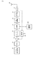
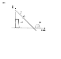
まず、従来技術の問題点について改めて説明する。デジタルベースバンド信号をアナログベースバンド信号に変換するDACの出力には、図2に示すように送信すべき信号成分22のほか、サンプリング周波数の整数倍の周波数近辺に不要成分23及び24が存在する。これらの不要成分23及び24はエイリアス成分またはイメージ成分と呼ばれる。
Next, the operation and advantages of the wireless transmitter according to the present embodiment will be described in detail.
First, the problems of the prior art will be described again. In the output of the DAC that converts a digital baseband signal into an analog baseband signal, there are
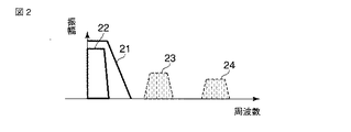
従来技術によると、これらの不要成分23及び24は図2に示すような低域を通過域とする周波数特性21を持つベースバンドフィルタによって除去される。ベースバンドフィルタの出力信号は直交変調器に入力され、直交変調器から出力される被変調信号は、電力増幅器を経て図3に示すような周波数特性31を持ち、信号成分32のみを通過させる高周波フィルタによって、高調波の不要成分が除去されてからアンテナに送られる。DACの出力に現れる高調波成分は、高周波フィルタの出力では図3に示す不要成分33〜36となって現れる。DACの出力側にベースバンドフィルタがあれば、高周波フィルタの通過域に存在する不要成分34及び35は周波数フィルタによって除去される。
According to the prior art, these
一方、特許文献1では高オーバサンプリングDACを用いることにより、図4に示すようにDACから出力される不要成分37及び38を高周波フィルタの通過域の外に出すことで、ベースバンドフィルタを省略している。しかし、特許文献1の技術ではDACで用いるクロック信号の周波数と変調器で用いる搬送波信号の周波数によっては、DACで発生する、クロック信号の高調波成分と、搬送波信号または搬送波信号の高調波成分との混合成分が送信RF信号の周波数に近くなる。この混合成分は本来の送信RF信号と同様に増幅され、アンテナから放射されてしまう。
On the other hand, in
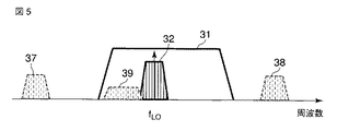
例えば、クロック信号の周波数が110MHz、搬送波信号の周波数が830MHzの場合、110MHz×15−830MHz=820MHzとなり、この820MHzの差周波数成分が図5に示すように高周波フィルタの帯域内にエイリアス成分39として混入してしまう。ここでは、クロック信号の高調波成分と搬送波信号の基本波成分との混合成分(差周波数成分)が高周波フィルタの帯域内にエイリアス成分として混入する例を示したが、クロック信号の高調波成分と搬送波信号の高調波成分との混合成分がエイリアス成分となる場合もある。
For example, when the frequency of the clock signal is 110 MHz and the frequency of the carrier wave signal is 830 MHz, 110 MHz × 15−830 MHz = 820 MHz, and the difference frequency component of 820 MHz is an
本実施形態によると、(a)占有面積の大きいベースバンドフィルタを用いることなく、あるいはベースバンドフィルタを簡略化しつつ、(b)DACのクロック信号の高調波成分と搬送波信号または搬送波信号の高調波成分との混合成分による、高周波フィルタで除去できない不要成分の発生を避ける、という効果を得ることができる。以下、その理由について詳しく述べる。 According to this embodiment, (a) without using a baseband filter having a large occupied area or simplifying the baseband filter, (b) harmonic components of the clock signal of the DAC and harmonics of the carrier signal or the carrier signal. The effect of avoiding the generation of unnecessary components that cannot be removed by the high-frequency filter due to the mixed components with the components can be obtained. Hereinafter, the reason will be described in detail.
まず、本実施形態において(a)のベースバンドフィルタを必要としない、あるいはベースバンドフィルタを簡略化できる理由は、以下の通りである。
デジタル回路の消費電力は、クロック周波数に反比例して減少する。そこで、背景技術の項で述べたように、従来では送信すべきデジタルベースバンド信号に対して低いサンプルレートでデジタル−アナログ変換を行い、デジタル−アナログ変換に伴う高調波成分をアナログベースバンドフィルタで除去することでエイリアスの発生を防止する手法がとられてきた。
First, the reason why the baseband filter (a) is not necessary or can be simplified in the present embodiment is as follows.
The power consumption of the digital circuit decreases in inverse proportion to the clock frequency. Therefore, as described in the background section, conventionally, digital baseband signals to be transmitted are subjected to digital-analog conversion at a low sample rate, and harmonic components accompanying the digital-analog conversion are converted to analog baseband filters. Techniques have been taken to prevent aliasing by removing them.
一方、本実施形態では半導体微細加工技術の進歩によりデジタル回路やDACの高速化が容易になってきたことを利用して、DAC11を高速クロックで、具体的には前述のように高周波フィルタ16の通過帯域幅より高い周波数のクロック信号で動作させる。これにより高周波フィルタ16によって、エイリアスとなる不要成分の発生を避け、ベースバンドフィルタを著しく簡略化するか、もしくはベースバンドフィルタを用いないようにすることができる。
On the other hand, in the present embodiment, the advancement of the semiconductor microfabrication technology makes it easy to increase the speed of digital circuits and DACs. Operate with a clock signal with a frequency higher than the passband width. As a result, the high-
次に、本実施形態による(b)の効果は以下のように説明される。図1の送信機において、ループフィルタ13は例えば積分器のように低い周波数で高い利得を有するアクティブフィルタが用いられ、これによりフィードバックループは高いループ利得を持つようになる。このため変調器14及び電力増幅器16で発生する雑音や誤差は、フィードバックループのループ利得の効果により圧縮される。例えば、変調器14において発生する不要成分として、DAC11で発生されかつループフィルタ13を通過する、クロック信号の高調波成分と搬送波信号または搬送波信号の高調波成分との混合成分について考える。
Next, the effect of (b) by this embodiment is demonstrated as follows. In the transmitter of FIG. 1, an active filter having a high gain at a low frequency, such as an integrator, is used as the
まず、ループフィルタ13の周波数特性そのものによって、DAC11で発生する高い周波数の不要成分を除去する効果が得られる。さらに、変調器14において不要成分が搬送波信号との混合により低い周波数のエイリアス成分に変換されたとしても、フィードバックループの高いループ利得による不要成分の抑制効果が期待できる。
First, the effect of removing unnecessary components of high frequency generated in the DAC 11 is obtained by the frequency characteristics of the
このようにループフィルタ13の周波数特性とループ利得の両方の効果によって、DAC11で発生する不要成分そのものや、その不要成分がループフィルタ13を通過して出力される高調波成分と搬送波信号または搬送波信号の高調波成分との混合成分の影響を低減できる。すなわち、このような混合成分が図5に示したように所望信号の帯域付近に現れるような現象は避けられ、結果的に図4に示したと同様の特性が実現される。
Thus, due to the effects of both the frequency characteristics and the loop gain of the
図1のようなフィードバックループを有しない、すなわちフィードフォワードパスのみを有する無線送信機では、たとえDACのサンプルレートを高くしても、DACで発生するエイリアス成分と搬送波信号または搬送波信号の高調波成分との混合成分が高周波フィルタの帯域内に存在する可能性がある。従って、DACの出力からエイリアス成分を除去するためにベースバンドフィルタは必要であった。これに対し、本実施形態に従う無線送信機はフィードバックループを備えることで、高調波同士の乗算により生じた不要成分を抑制し、ベースバンドアナログフィルタの著しい簡素化を実現するものである。 In a radio transmitter having no feedback loop as shown in FIG. 1, that is, having only a feed forward path, even if the DAC sample rate is increased, the alias component generated in the DAC and the harmonic component of the carrier signal or the carrier signal May be present in the band of the high-frequency filter. Therefore, a baseband filter was necessary to remove the alias component from the DAC output. On the other hand, the wireless transmitter according to the present embodiment includes a feedback loop, thereby suppressing unnecessary components generated by multiplication of harmonics and realizing a significant simplification of the baseband analog filter.
本実施形態では、上述のようにDAC11の出力信号から高調波成分を除去するベースバンドフィルタ(アンチエイリアスフィルタ)を用いない代わりに、ループフィルタ13を必要としている。ここで、従来のベースバンドフィルタは通過域において平坦な周波数特性を実現しつつ、阻止域で必要な減衰量を確保する必要があるため、簡素な回路での実現は困難であった。一方、本実施形態で用いるループフィルタ13はベースバンドフィルタに要求されるような利得の平坦性は必要でない。
In the present embodiment, the
例えば、積分器は図6の周波数特性41に示されるように、入力信号42の帯域(通過域)では十分高い利得を有し、ベースバンドフィルタのような通過域での平坦性は持たない。一方、このような特性を持つ積分器をループフィルタ13に用いると、フィードバックループの効果が働き、ループ利得が十分高い周波数ではフィードバックパスの利得によって全体の利得が決定されるため、図6の点線43で示される平坦な周波数特性を容易に実現できる。また、図6に示されるようにDAC11で発生する不要成分44は、ループフィルタ13の阻止域にあるため、エイリアスとはならない。
For example, the integrator has a sufficiently high gain in the band (pass band) of the
このようにループフィルタ13としては、積分器のような簡素な回路を利用することが可能である。このため、特に送信機を集積回路により実現する場合、チップの面積を削減することができる。ループフィルタの実現法として、積分器を多段接続する手法や、積分器に代えて特定の周波数で高い利得をもつ共振特性を持たせたりする手法は、ΔΣ変調型ADCの試作例として数多くの報告がある。これらの手法を本実施形態におけるループフィルタ13に適用することによって、不要成分を抑圧可能な周波数範囲を拡大することも容易である。
Thus, as the
(第2の実施形態)
図7は、本発明の第2の実施形態に従う無線送信機を示している。第2の実施形態と図1に示した第1の実施形態との違いは、第2の実施形態では電力分岐器17が電力増幅器15と高周波フィルタ16との間にあり、高周波フィルタ16がフィードバックループの外にあることである。すなわち、本実施形態では電力分岐器17によって電力増幅器15から出力される増幅された被変調信号の一部の電力が分岐され、フィードバック被変調信号として復調器19に入力される。復調器19では、フィードバック被変調信号に対して搬送波発生器18からの搬送波信号を用いて復調が行われ、フィードバックベースバンド信号が生成される。
(Second Embodiment)
FIG. 7 shows a wireless transmitter according to the second embodiment of the present invention. The difference between the second embodiment and the first embodiment shown in FIG. 1 is that, in the second embodiment, the
高周波フィルタ16の特性があまり良好でない場合、特に群遅延が大きい場合には、高周波フィルタがフィードバックループ内にあるとループの安定性が低下し、ループが正常に動作しない場合がある。本実施形態によると、高周波フィルタ16をループの外に置くことにより、高周波フィルタ16の群遅延特性が良好でない場合でも、上記のような弊害が避けられる。
When the characteristics of the high-
本実施形態における電力増幅器15としては、例えば特定の周波数成分のみを増幅する特性を持つ、いわゆる同調増幅器が用いられる。従って、電力増幅器15においてもある程度不要成分の除去が行われるので、電力増幅器15の出力信号をフィードバック信号として利用することが可能な場合もある。ただし、通常は電力増幅器15に同調増幅器を用いてもその出力信号は残留した不要成分を含むため、送信機からの不要輻射を防止する上では、アンテナ20に供給する送信RF信号としては好ましくない。そこで、このような残留した不要成分を取り除くために、高周波フィルタ16を用いることが望ましい。
As the
(各要素の具体例)
次に、図8〜図12を用いて図1及び図7中に示した各要素、特に変調器14、復調器19及びDAC11の具体例について述べる。
(Specific examples of each element)
Next, specific examples of each element shown in FIGS. 1 and 7, particularly the
現在、多くのデジタル通信方式では、信号の振幅と位相の両方を変調する方式が採用されている。すなわち、送受信される信号は直交座標で表現された直交信号であるIチャネル信号及びQチャネル信号として扱われる。このような場合、図1及び図7に示した無線送信機において、デジタル信号生成部10によって生成されるデジタルベースバンド信号、DAC11から出力されるアナログベースバンド信号、減算器12から出力される残差信号、ループフィルタ13から出力されるフィルタ信号、及び復調器19から出力されるフィードバックベースバンド信号は、いずれも直交信号であるIチャネル信号及びQチャネル信号で表現される。さらに、変調器14として直交変調器が使用され、復調器19として直交復調器が使用される。
Currently, many digital communication systems employ a system that modulates both the amplitude and phase of a signal. That is, signals to be transmitted and received are treated as I channel signals and Q channel signals that are orthogonal signals expressed in orthogonal coordinates. In such a case, in the wireless transmitter shown in FIGS. 1 and 7, the digital baseband signal generated by the digital
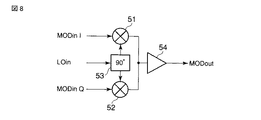
<直交変調器>
図8は、変調器14として使用可能な直交変調器の例であり、二つの乗算器(ミキサ)51及び52、90°移相器53、及び出力バッファ54を有する。変調器14である直交変調器には、図1または図7中に示したループフィルタ13からのフィルタ信号である変調すべきIチャネル信号MODinI及びQチャネル信号MODinQと、図1または図7中に示した搬送波発生器18からの搬送波信号(ローカル信号)LOinが入力される。ローカル信号LOinは、90°移相器53により互いに90°の位相差を有する搬送波信号とされる。
<Quadrature modulator>
FIG. 8 is an example of a quadrature modulator that can be used as the
乗算器51及び52において、90°の位相差を持つ二つのローカル信号はIチャネル信号MODinI及びQチャネル信号MODinQによりそれぞれ振幅変調された後に加算され、出力バッファ54を介して被変調信号として出力される。Iチャネル信号とQチャネル信号の振幅の比によって、出力バッファ54から出力される被変調信号の位相が制御され、振幅と位相の変調が実現される。
In the
<直交復調器>
図9は、フィードバックパスに挿入される復調器19として使用可能な直交復調器の例であり、二つの乗算器(ミキサ)61及び62、90°移相器63、及び入力バッファ64を有する。復調器19である直交復調器には、図1中に示した電力分岐器17からの送信RF信号(または図7中に示した電力分岐器17からの増幅された被変調信号)RFinと、図1または図7中に示した搬送波発生器18からの搬送波信号(ローカル信号)LOinが入力される。ローカル信号LOinは、90°移相器63により互いに90°の位相差を有する搬送波信号とされる。
<Quadrature demodulator>
FIG. 9 is an example of a quadrature demodulator that can be used as the
信号RFinは入力バッファ64を介して乗算器61及び62に入力され、90°の位相差を持つ二つの搬送波信号と乗算されることにより復調され、フィードバックベースバンド信号であるIチャネル信号DEMoutI及びQチャネル信号DEMoutQが生成される。
The signal RFin is input to the
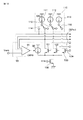
<三相変調器>
図1及び図7に示した無線送信機において、デジタル信号生成部10で生成されるデジタルベースバンド信号、DAC11から出力されるアナログベースバンド信号、減算器12から出力される残差信号、ループフィルタ13から出力されるフィルタ信号、及び復調器19から出力されるフィードバックベースバンド信号は、上述のように直交信号でもよいが、特開2007−043290号公報に記載されているように、三相平衡信号(三相信号)であってもよい。
<Three-phase modulator>
1 and 7, the digital baseband signal generated by the
一般に、無線送信機を集積回路により実現する場合には、直交信号をそれぞれ正と負の2端子間の電圧により表現する差動方式を採用することが多い。このため、4端子を用いて2信号を表現する回路が採用されている。しかしもこの回路は冗長であり、2次元の信号は3端子を用いることで表現可能である。極端には、3端子のうち1端子を基準電位とし、残り2端子の電位で信号を表現することも可能であるが、集積回路上で変動が小さい基準電位を作ることは困難である。2端子の差動回路がその2端子の電位の平均値(共通モード電圧と呼ばれる)を基準電位として用いているように、3端子の平均値を基準電位とする平衡三相方式であれば、差動回路の拡張により実現可能である。 In general, when a wireless transmitter is realized by an integrated circuit, a differential method in which orthogonal signals are expressed by voltages between two positive and negative terminals is often employed. For this reason, a circuit that expresses two signals using four terminals is employed. However, this circuit is redundant, and a two-dimensional signal can be expressed by using three terminals. In an extreme case, one of the three terminals can be used as a reference potential, and a signal can be expressed by the potential of the remaining two terminals. However, it is difficult to create a reference potential with little fluctuation on an integrated circuit. If the two-terminal differential circuit uses the average value of the two-terminal potential (referred to as a common mode voltage) as the reference potential, and if it is a balanced three-phase system with the average value of the three terminals as the reference potential, This can be realized by expanding the differential circuit.
図10は、このような考えに基づく変調器14として使用可能な三相変調器の例を示している。変調器14である三相変調器には、図1または図7中に示したループフィルタ13からのフィルタ信号である変調すべき三相の変調信号MODin1,MODin2及びMODin3と、図1または図7中に示した搬送波発生器18からの三相の搬送波信号(ローカル信号)LOin1,LOin2及びLOin3が入力される。
FIG. 10 shows an example of a three-phase modulator that can be used as the
変調信号MODin1,MODin2及びMODin3は、N型MOSトランジスタ(NMOSトランジスタ)71,72及び73のゲートに与えられる。ローカル信号LOin1,LOin2及びLOin3は、トランジスタ74,75及び76のゲートに与えられる。トランジスタ71,72及び73の共通ドレインは、負荷のインダクタ77を介して電源Vddに接続されると共に、キャパシタ78を介して出力端子に接続される。トランジスタ71,72及び73のソースはトランジスタ74,75及び76のドレインに接続され、トランジスタ74,75及び76のソースはグラウンドGNDに接続される。このような構成により、出力端子から被変調信号MODoutが出力される。
Modulation signals MODin1, MODin2, and MODin3 are applied to gates of N-type MOS transistors (NMOS transistors) 71, 72, and 73, respectively. Local signals LOin1, LOin2, and LOin3 are applied to the gates of
<三相復調器>
図11は、フィードバックパスに挿入される復調器19として使用可能な三相復調器の例であり、差動増幅回路形の周波数変換回路を3相に拡張したものである。復調器19である三相復調器には、図1中に示した電力分岐器17からの送信RF信号(または図7中に示した電力分岐器17からの増幅された被変調信号)RFinと、図1または図7中に示した搬送波発生器18からの三相の搬送波信号(ローカル信号)LOin1,LOin2及びLOin3が入力される。
<Three-phase demodulator>
FIG. 11 shows an example of a three-phase demodulator that can be used as the
ローカル信号LOin1,LOin2及びLOin3は、NMOSトランジスタ81,82及び83のゲートに与えられる。被変調信号RFinは、NMOSトランジスタ80のゲートに与えられる。トランジスタ81,82及び83のドレインは、それぞれ負荷抵抗84,85及び86を介して電源Vddに接続されると共に、三相出力端子に接続される。トランジスタ81,82及び83の共通ソースはトランジスタ80のドレインに接続され、トランジスタ80のソースはグラウンドGNDに接続される。このような構成によって、三相出力端子から三相のフィードバックベースバンド信号DEMout1,DEMout2及びDEMout3が得られる。
Local signals LOin1, LOin2, and LOin3 are applied to the gates of
<電流出力型DAC及び電流出力型復調器>
図1または図7に示した無線送信機において、DAC11と復調器19を共に電流出力型とすることにより、減算器12を結線により実現することができる。図12は、そのような例を示す電流出力型三相DAC110と電流出力型三相復調器を示している。DAC11に相当する電流出力型三相DAC110は、電流値の異なる電流源111,112及び113と、デジタル値(デジタルベースバンド信号の値)に応じてスイッチングされるスイッチ114,115及び116を含み、図1または図7中に示したデジタル信号生成部10からのデジタルベースバンド信号に対応したアナログベースバンド信号を電流信号として出力する。
<Current output type DAC and current output type demodulator>
In the wireless transmitter shown in FIG. 1 or FIG. 7, the
一方、復調器19に相当する電流出力型三相復調器は、NMOSトランジスタ100,101,102及び103を含む。図1中に示した電力分岐器17からの送信RF信号(または図7中に示した電力分岐器17からの増幅された被変調信号)RFinは、トランジスタ100のゲートに入力され、図1または図7中に示した搬送波発生器18からの三相の搬送波信号(ローカル信号)LOin1,LOin2及びLOin3は、トランジスタ101,102及び103のゲートに入力される。電流出力型三相復調器の出力端子であるトランジスタ101,102及び103のドレインは、電流出力型三相DAC110の出力端子と共通に接続される。
On the other hand, a current output type three-phase demodulator corresponding to the
このようにDAC11及び復調器19を共に電流出力型構成とし、互いの出力端子を共通に接続することにより、それぞれの出力である電流信号の減算を行い、三相の残差信号DEFoutを得ることができる。すなわち、図1または図7中に示した減算器12の機能が結線により実現される。
In this way, both the DAC 11 and the
DAC11及び復調器19を共に電流出力型とした場合、それぞれのバイアス電流は必ずしも一致しないため、単純にそれぞれの出力端子を共通に接続したのでは正しい減算ができない。そこで、図12では演算増幅器91と電流源92による公知の共通モードフィードバック(CMFB)回路90を用いて、DAC及び復調器のバイアス電流の差に相当する電流を供給すると共に、三相の残差信号DEFoutの平均電圧が参照電圧Vcomに近い値となるような制御が行われる。
When both the DAC 11 and the
図12の例では、三相の電流出力型DAC及び三相の電流出力型復調器について示したが、DAC11及び復調器19は共に単相の電流出力型の場合でも、同様にそれぞれの出力端子を共通に接続することで、電流信号で減算を行うことができる。
In the example of FIG. 12, the three-phase current output type DAC and the three-phase current output type demodulator are shown. However, even if both the DAC 11 and the
以上の実施形態では無線送信機について述べたが、本発明は例えば周波数分割多重方式を用いた有線通信用の送信機として用いることも可能である。また、本発明は上記実施形態そのままに限定されるものではなく、実施段階ではその要旨を逸脱しない範囲で構成要素を変形して具体化できる。さらに、上記実施形態に開示されている複数の構成要素の適宜な組み合わせにより、種々の発明を形成できる。例えば、実施形態に示される全構成要素から幾つかの構成要素を削除してもよい。 Although the wireless transmitter has been described in the above embodiments, the present invention can also be used as a transmitter for wired communication using, for example, a frequency division multiplexing system. Further, the present invention is not limited to the above-described embodiment as it is, and can be embodied by modifying the constituent elements without departing from the scope of the invention in the implementation stage. Furthermore, various inventions can be formed by appropriately combining a plurality of constituent elements disclosed in the embodiment. For example, some components may be deleted from all the components shown in the embodiment.
10・・・デジタル信号生成部
11・・デジタル−アナログ変換器
12・・・減算器
13・・・ループフィルタ
14・・・変調器
15・・・電力増幅器
16・・・高周波フィルタ
17・・・電力分岐器
18・・・搬送波発生器
19・・・復調器
20・・・アンテナ
DESCRIPTION OF
Claims (10)
所定周波数のクロック信号に従って動作し、前記デジタルベースバンド信号をアナログベースバンド信号に変換するデジタル−アナログ変換器と、
前記アナログベースバンド信号からフィードバックベースバンド信号を差し引いた残差信号の低域成分を増幅するとともに前記残差信号の高域成分を抑圧してフィルタ信号を生成するループフィルタと、
前記フィルタ信号に対して搬送波信号を乗じることにより変調を行い、被変調信号を生成する変調器と、
前記被変調信号を増幅する電力増幅器と、
前記クロック信号の周波数より狭い通過帯域幅を持ち、前記被変調信号に含まれる不要成分の少なくとも一部を除去して送信RF信号を得る高周波フィルタと、
前記送信RF信号から分岐されたフィードバックRF信号に対して前記搬送波信号を用いて復調を行い、前記フィードバックベースバンド信号を生成する復調器と、
を具備する送信機。 A signal generator for generating a digital baseband signal corresponding to the signal to be transmitted;
A digital-analog converter that operates according to a clock signal of a predetermined frequency and converts the digital baseband signal into an analog baseband signal;
A loop filter that amplifies a low-frequency component of a residual signal obtained by subtracting a feedback baseband signal from the analog baseband signal and generates a filter signal by suppressing a high-frequency component of the residual signal;
A modulator for performing modulation by multiplying the filter signal by a carrier signal, and generating a modulated signal;
A power amplifier for amplifying the modulated signal;
A high-frequency filter having a pass bandwidth narrower than the frequency of the clock signal and obtaining a transmission RF signal by removing at least a part of unnecessary components contained in the modulated signal;
A demodulator that demodulates the feedback RF signal branched from the transmission RF signal using the carrier signal and generates the feedback baseband signal;
A transmitter comprising:
所定周波数のクロック信号に従って動作し、前記デジタルベースバンド信号をアナログベースバンド信号に変換するデジタル−アナログ変換器と、
前記アナログベースバンド信号からフィードバックベースバンド信号を差し引いた残差信号の低域成分を増幅するとともに前記残差信号の高域成分を抑圧してフィルタ信号を生成するループフィルタと、
前記フィルタ信号に対して搬送波信号を乗じることにより変調を行い、被変調信号を生成する変調器と、
前記被変調信号を増幅する電力増幅器と、
前記増幅された被変調信号から分岐されたフィードバック被変調信号に対して前記搬送波信号を用いて復調を行い、前記フィードバックベースバンド信号を生成する復調器と、
前記クロック信号の周波数より狭い通過帯域幅を持ち、増幅された被変調信号に含まれる不要成分を除去して送信RF信号を得る高周波フィルタと、
を具備する送信機。 A signal generator for generating a digital baseband signal corresponding to the signal to be transmitted;
A digital-analog converter that operates according to a clock signal of a predetermined frequency and converts the digital baseband signal into an analog baseband signal;
A loop filter for amplifying a low-frequency component of a residual signal obtained by subtracting a feedback baseband signal from the analog baseband signal and generating a filter signal by suppressing the high-frequency component of the residual signal;
A modulator for performing modulation by multiplying the filter signal by a carrier signal, and generating a modulated signal;
A power amplifier for amplifying the modulated signal;
A demodulator that demodulates the feedback modulated signal branched from the amplified modulated signal using the carrier signal and generates the feedback baseband signal;
A high-frequency filter having a pass bandwidth narrower than the frequency of the clock signal and obtaining a transmission RF signal by removing unnecessary components contained in the amplified modulated signal;
A transmitter comprising:
前記復調器は、前記フィードバックベースバンド信号を第2の電流信号として少なくとも一つの第2出力端子から出力するように構成され、
前記第1出力端子と前記第2の出力端子とは共通に接続されており、これによって前記第1の電流信号から前記第2の電流信号が差し引かれ、前記残差信号が生成される請求項1または3のいずれか1項記載の送信機。 The digital-analog converter is configured to output the analog baseband signal as a first current signal from at least one first output terminal;
The demodulator is configured to output the feedback baseband signal as a second current signal from at least one second output terminal;
The first output terminal and the second output terminal are connected in common, whereby the second current signal is subtracted from the first current signal to generate the residual signal. The transmitter according to any one of 1 and 3.
Priority Applications (2)
| Application Number | Priority Date | Filing Date | Title |
|---|---|---|---|
| JP2008078739A JP2009232425A (en) | 2008-03-25 | 2008-03-25 | Transmitter |
| US12/403,534 US20090245418A1 (en) | 2008-03-25 | 2009-03-13 | Transmitter using cartesian loop |
Applications Claiming Priority (1)
| Application Number | Priority Date | Filing Date | Title |
|---|---|---|---|
| JP2008078739A JP2009232425A (en) | 2008-03-25 | 2008-03-25 | Transmitter |
Publications (1)
| Publication Number | Publication Date |
|---|---|
| JP2009232425A true JP2009232425A (en) | 2009-10-08 |
Family
ID=41117180
Family Applications (1)
| Application Number | Title | Priority Date | Filing Date |
|---|---|---|---|
| JP2008078739A Withdrawn JP2009232425A (en) | 2008-03-25 | 2008-03-25 | Transmitter |
Country Status (2)
| Country | Link |
|---|---|
| US (1) | US20090245418A1 (en) |
| JP (1) | JP2009232425A (en) |
Families Citing this family (5)
| Publication number | Priority date | Publication date | Assignee | Title |
|---|---|---|---|---|
| CN101860502B (en) * | 2010-04-14 | 2016-01-27 | 中国科学院计算技术研究所 | A kind of method and apparatus detecting LTE system duplex mode |
| US8803627B1 (en) * | 2013-12-03 | 2014-08-12 | Innophase Inc. | Wideband direct DCO modulator with in-band compensation |
| CN105471427B (en) * | 2014-09-04 | 2019-07-26 | 中芯国际集成电路制造(上海)有限公司 | A kind of multi-modulus frequency divider and electronic device |
| CN109150211B (en) * | 2017-06-19 | 2020-09-25 | 大唐移动通信设备有限公司 | Broadband transmitting device |
| JP2021074080A (en) * | 2019-11-06 | 2021-05-20 | ソニーセミコンダクタソリューションズ株式会社 | Signal processing circuit |
Family Cites Families (16)
| Publication number | Priority date | Publication date | Assignee | Title |
|---|---|---|---|---|
| US5767750A (en) * | 1992-03-30 | 1998-06-16 | Kabushiki Kaisha Toshiba | Modulator |
| JP3419484B2 (en) * | 1992-03-30 | 2003-06-23 | 株式会社東芝 | Modulator, transmitter |
| JP4086133B2 (en) * | 1999-07-28 | 2008-05-14 | 富士通株式会社 | Wireless device distortion compensation method and distortion compensation device |
| US6693956B1 (en) * | 1999-10-08 | 2004-02-17 | Hitachi Denshi Kabushiki Kaisha | Power amplifier having negative feedback circuit for transmitter |
| JP2002223130A (en) * | 2001-01-25 | 2002-08-09 | Fujitsu Ltd | Transmission device and transmission method |
| JP3880329B2 (en) * | 2001-04-20 | 2007-02-14 | 株式会社日立国際電気 | Loop gain control method and power amplifier circuit |
| US6853246B2 (en) * | 2002-04-18 | 2005-02-08 | Agere Systems Inc. | Adaptive predistortion system and a method of adaptively predistorting a signal |
| US6842486B2 (en) * | 2003-01-21 | 2005-01-11 | Cirrus Logic, Inc. | Signal processing system with baseband noise modulation and noise fold back reduction |
| US6961385B2 (en) * | 2003-01-21 | 2005-11-01 | Cirrus Logic, Inc. | Signal processing system with baseband noise modulation chopper circuit timing to reduce noise |
| US7593695B2 (en) * | 2005-03-15 | 2009-09-22 | Broadcom Corporation | RF transceiver incorporating dual-use PLL frequency synthesizer |
| CN101228690B (en) * | 2005-07-29 | 2010-08-18 | 富士通株式会社 | delay adjustment device |
| DE602006001356D1 (en) * | 2006-02-06 | 2008-07-10 | Alcatel Lucent | Modular multiband, multi-standard transceiver circuit for mobile and base stations of radio communication systems |
| JP4155588B2 (en) * | 2006-05-31 | 2008-09-24 | 株式会社東芝 | Digital / analog converter and transmitter |
| US7639992B2 (en) * | 2006-12-21 | 2009-12-29 | Broadcom Corporation | Digital compensation for nonlinearities in a phase-locked loop of a polar transmitter |
| US7822131B2 (en) * | 2007-01-03 | 2010-10-26 | Freescale Semiconductor, Inc. | Reducing a peak-to-average ratio of a signal |
| US7890067B2 (en) * | 2007-05-10 | 2011-02-15 | Pine Valley Investments, Inc. | Linear RF amplifier with polar feedback |
-
2008
- 2008-03-25 JP JP2008078739A patent/JP2009232425A/en not_active Withdrawn
-
2009
- 2009-03-13 US US12/403,534 patent/US20090245418A1/en not_active Abandoned
Also Published As
| Publication number | Publication date |
|---|---|
| US20090245418A1 (en) | 2009-10-01 |
Similar Documents
| Publication | Publication Date | Title |
|---|---|---|
| CN100517985C (en) | Transmission circuit and transmitter/receiver using same | |
| KR102492442B1 (en) | Method and apparatus to detect lo leakage and image rejection using a single transistor | |
| KR101717311B1 (en) | Rf amplifier with digital filter for polar transmitter | |
| US20060178120A1 (en) | Transmitting/receiving device having a polar modulator with variable predistortion | |
| JP4464194B2 (en) | Communication receiver and transmitter | |
| US9596120B2 (en) | Signal transmission apparatus, distortion compensation apparatus, and signal transmission method | |
| JP6344394B2 (en) | Transmitter and control method thereof | |
| JP2005020694A (en) | Multi-mode multi-amplifier architecture | |
| US10326482B2 (en) | Linearization of a radiofrequency-signal transmission chain | |
| KR20060136227A (en) | Doherty Amplifier and Transmitter Using Mixer | |
| US20110254636A1 (en) | Multi-phase pulse modulation polar transmitter and method of generating a pulse modulated envelope signal carrying modulated rf signal | |
| JP2009232425A (en) | Transmitter | |
| US8023923B2 (en) | Mixer circuit | |
| US7454184B2 (en) | DC offset cancellation in a wireless receiver | |
| US20120002755A1 (en) | Multi-level pulse modulated polar transmitter and method of generating multi-level modulated envelope signals carrying modulated rf signal | |
| JP5347892B2 (en) | Transmitter | |
| US8648655B2 (en) | Modulator and an amplifier using the same | |
| CN107046406B (en) | Outphasing amplifier | |
| JP5731325B2 (en) | Modulator and amplifier using the same | |
| CN103546404A (en) | Direct conversion transceiver for compensating DC offset and operation method thereof | |
| US9020450B2 (en) | Output stage for wireless transmitter | |
| JP2013051456A5 (en) | ||
| US12231143B2 (en) | Radio transmitter providing an analog signal with both radio frequency and baseband frequency information | |
| JP2006121408A (en) | Modulation signal transmission circuit and radio communication apparatus | |
| JP2018125712A (en) | Transmitter and signal generation method |
Legal Events
| Date | Code | Title | Description |
|---|---|---|---|
| A300 | Application deemed to be withdrawn because no request for examination was validly filed |
Free format text: JAPANESE INTERMEDIATE CODE: A300 Effective date: 20110607 |