JP2009260366A - 半導体装置及びその作製方法 - Google Patents
半導体装置及びその作製方法 Download PDFInfo
- Publication number
- JP2009260366A JP2009260366A JP2009151783A JP2009151783A JP2009260366A JP 2009260366 A JP2009260366 A JP 2009260366A JP 2009151783 A JP2009151783 A JP 2009151783A JP 2009151783 A JP2009151783 A JP 2009151783A JP 2009260366 A JP2009260366 A JP 2009260366A
- Authority
- JP
- Japan
- Prior art keywords
- semiconductor film
- insulating film
- film
- semiconductor
- convex portion
- Prior art date
- Legal status (The legal status is an assumption and is not a legal conclusion. Google has not performed a legal analysis and makes no representation as to the accuracy of the status listed.)
- Granted
Links
Images





Classifications
-
- H—ELECTRICITY
- H10—SEMICONDUCTOR DEVICES; ELECTRIC SOLID-STATE DEVICES NOT OTHERWISE PROVIDED FOR
- H10D—INORGANIC ELECTRIC SEMICONDUCTOR DEVICES
- H10D30/00—Field-effect transistors [FET]
- H10D30/01—Manufacture or treatment
- H10D30/021—Manufacture or treatment of FETs having insulated gates [IGFET]
- H10D30/031—Manufacture or treatment of FETs having insulated gates [IGFET] of thin-film transistors [TFT]
- H10D30/0321—Manufacture or treatment of FETs having insulated gates [IGFET] of thin-film transistors [TFT] comprising silicon, e.g. amorphous silicon or polysilicon
-
- H—ELECTRICITY
- H10—SEMICONDUCTOR DEVICES; ELECTRIC SOLID-STATE DEVICES NOT OTHERWISE PROVIDED FOR
- H10D—INORGANIC ELECTRIC SEMICONDUCTOR DEVICES
- H10D30/00—Field-effect transistors [FET]
- H10D30/01—Manufacture or treatment
- H10D30/021—Manufacture or treatment of FETs having insulated gates [IGFET]
- H10D30/031—Manufacture or treatment of FETs having insulated gates [IGFET] of thin-film transistors [TFT]
- H10D30/0312—Manufacture or treatment of FETs having insulated gates [IGFET] of thin-film transistors [TFT] characterised by the gate electrodes
- H10D30/0314—Manufacture or treatment of FETs having insulated gates [IGFET] of thin-film transistors [TFT] characterised by the gate electrodes of lateral top-gate TFTs comprising only a single gate
-
- H—ELECTRICITY
- H10—SEMICONDUCTOR DEVICES; ELECTRIC SOLID-STATE DEVICES NOT OTHERWISE PROVIDED FOR
- H10D—INORGANIC ELECTRIC SEMICONDUCTOR DEVICES
- H10D30/00—Field-effect transistors [FET]
- H10D30/60—Insulated-gate field-effect transistors [IGFET]
- H10D30/67—Thin-film transistors [TFT]
- H10D30/6729—Thin-film transistors [TFT] characterised by the electrodes
- H10D30/673—Thin-film transistors [TFT] characterised by the electrodes characterised by the shapes, relative sizes or dispositions of the gate electrodes
- H10D30/6731—Top-gate only TFTs
-
- H—ELECTRICITY
- H10—SEMICONDUCTOR DEVICES; ELECTRIC SOLID-STATE DEVICES NOT OTHERWISE PROVIDED FOR
- H10D—INORGANIC ELECTRIC SEMICONDUCTOR DEVICES
- H10D30/00—Field-effect transistors [FET]
- H10D30/60—Insulated-gate field-effect transistors [IGFET]
- H10D30/67—Thin-film transistors [TFT]
- H10D30/674—Thin-film transistors [TFT] characterised by the active materials
- H10D30/6741—Group IV materials, e.g. germanium or silicon carbide
- H10D30/6743—Silicon
- H10D30/6745—Polycrystalline or microcrystalline silicon
-
- H—ELECTRICITY
- H10—SEMICONDUCTOR DEVICES; ELECTRIC SOLID-STATE DEVICES NOT OTHERWISE PROVIDED FOR
- H10D—INORGANIC ELECTRIC SEMICONDUCTOR DEVICES
- H10D30/00—Field-effect transistors [FET]
- H10D30/60—Insulated-gate field-effect transistors [IGFET]
- H10D30/67—Thin-film transistors [TFT]
- H10D30/6757—Thin-film transistors [TFT] characterised by the structure of the channel, e.g. transverse or longitudinal shape or doping profile
-
- H—ELECTRICITY
- H10—SEMICONDUCTOR DEVICES; ELECTRIC SOLID-STATE DEVICES NOT OTHERWISE PROVIDED FOR
- H10D—INORGANIC ELECTRIC SEMICONDUCTOR DEVICES
- H10D86/00—Integrated devices formed in or on insulating or conducting substrates, e.g. formed in silicon-on-insulator [SOI] substrates or on stainless steel or glass substrates
-
- H—ELECTRICITY
- H10—SEMICONDUCTOR DEVICES; ELECTRIC SOLID-STATE DEVICES NOT OTHERWISE PROVIDED FOR
- H10D—INORGANIC ELECTRIC SEMICONDUCTOR DEVICES
- H10D86/00—Integrated devices formed in or on insulating or conducting substrates, e.g. formed in silicon-on-insulator [SOI] substrates or on stainless steel or glass substrates
- H10D86/01—Manufacture or treatment
- H10D86/021—Manufacture or treatment of multiple TFTs
- H10D86/0221—Manufacture or treatment of multiple TFTs comprising manufacture, treatment or patterning of TFT semiconductor bodies
- H10D86/0223—Manufacture or treatment of multiple TFTs comprising manufacture, treatment or patterning of TFT semiconductor bodies comprising crystallisation of amorphous, microcrystalline or polycrystalline semiconductor materials
- H10D86/0227—Manufacture or treatment of multiple TFTs comprising manufacture, treatment or patterning of TFT semiconductor bodies comprising crystallisation of amorphous, microcrystalline or polycrystalline semiconductor materials using structural arrangements to control crystal growth, e.g. placement of grain filters
-
- G—PHYSICS
- G02—OPTICS
- G02F—OPTICAL DEVICES OR ARRANGEMENTS FOR THE CONTROL OF LIGHT BY MODIFICATION OF THE OPTICAL PROPERTIES OF THE MEDIA OF THE ELEMENTS INVOLVED THEREIN; NON-LINEAR OPTICS; FREQUENCY-CHANGING OF LIGHT; OPTICAL LOGIC ELEMENTS; OPTICAL ANALOGUE/DIGITAL CONVERTERS
- G02F1/00—Devices or arrangements for the control of the intensity, colour, phase, polarisation or direction of light arriving from an independent light source, e.g. switching, gating or modulating; Non-linear optics
- G02F1/01—Devices or arrangements for the control of the intensity, colour, phase, polarisation or direction of light arriving from an independent light source, e.g. switching, gating or modulating; Non-linear optics for the control of the intensity, phase, polarisation or colour
- G02F1/13—Devices or arrangements for the control of the intensity, colour, phase, polarisation or direction of light arriving from an independent light source, e.g. switching, gating or modulating; Non-linear optics for the control of the intensity, phase, polarisation or colour based on liquid crystals, e.g. single liquid crystal display cells
- G02F1/133—Constructional arrangements; Operation of liquid crystal cells; Circuit arrangements
- G02F1/1333—Constructional arrangements; Manufacturing methods
- G02F1/133305—Flexible substrates, e.g. plastics, organic film
-
- G—PHYSICS
- G02—OPTICS
- G02F—OPTICAL DEVICES OR ARRANGEMENTS FOR THE CONTROL OF LIGHT BY MODIFICATION OF THE OPTICAL PROPERTIES OF THE MEDIA OF THE ELEMENTS INVOLVED THEREIN; NON-LINEAR OPTICS; FREQUENCY-CHANGING OF LIGHT; OPTICAL LOGIC ELEMENTS; OPTICAL ANALOGUE/DIGITAL CONVERTERS
- G02F1/00—Devices or arrangements for the control of the intensity, colour, phase, polarisation or direction of light arriving from an independent light source, e.g. switching, gating or modulating; Non-linear optics
- G02F1/01—Devices or arrangements for the control of the intensity, colour, phase, polarisation or direction of light arriving from an independent light source, e.g. switching, gating or modulating; Non-linear optics for the control of the intensity, phase, polarisation or colour
- G02F1/13—Devices or arrangements for the control of the intensity, colour, phase, polarisation or direction of light arriving from an independent light source, e.g. switching, gating or modulating; Non-linear optics for the control of the intensity, phase, polarisation or colour based on liquid crystals, e.g. single liquid crystal display cells
- G02F1/133—Constructional arrangements; Operation of liquid crystal cells; Circuit arrangements
- G02F1/1333—Constructional arrangements; Manufacturing methods
- G02F1/1345—Conductors connecting electrodes to cell terminals
- G02F1/13454—Drivers integrated on the active matrix substrate
Landscapes
- Thin Film Transistor (AREA)
- Recrystallisation Techniques (AREA)
Abstract
【解決手段】ソース領域及びドレイン領域を含む半導体膜と、半導体膜の側面に接して設けられた第1の絶縁膜と、半導体膜及び第1の絶縁膜上に設けられた第2の絶縁膜と、第2の絶縁膜上に設けられたゲート電極と、ゲート電極上に設けられた第3の絶縁膜と、第2の絶縁膜及び前記第3の絶縁膜に設けられ、半導体膜の一部及び前記第1の絶縁膜の一部を露出させる開口と、開口を介して半導体膜に電気的に接続する配線又は電極と、を有し、第1の絶縁膜は、半導体膜の側面に接する部分が一部エッチングされ窪んでおり、配線又は電極は、第1の絶縁膜の窪んだ部分に入り込んでいることを特徴とする。
【選択図】図15
Description
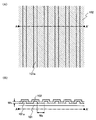
の破線A−A’における断面図に相当する。島状の半導体膜106は、凸部101a間に形成される凹部上にその一部が存在する。さらに、半導体膜106は、その一部が凸部101aと接している。TFTのチャネル形成領域は、半導体膜105の凹部上に位置する部分を用いて形成されるように、そのチャネル長、チャネル幅を考慮して、凸部101aのレイアウトを定めるのが望ましい。なお、ソース領域またはドレイン領域となる部分をも凹部上に存在する半導体膜で形成することで、ソース領域とドレイン領域の抵抗を下げることができる。
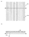
の破線C−C’における断面図に相当する。島状の半導体膜172は、チャネル形成領域となる部分と、ソース領域又はドレイン領域となる部分とで、厚さに差が生じている。またソース領域またはドレイン領域となる部分は、その一部が凸部101a上に重なっていても良い。
を7.13%とフッ化アンモニウム(NH4F)を15.4%含む混合溶液(ステラケミファ社製、商品名LAL500)をエッチャントとし、20℃においてウエットエッチングを行う。このエッチングにより、矩形状の凸部353が形成される。本明細書では、第1下地膜350と凸部353とを合わせて1つの下地膜とみなす。
なお、本実施例ではOLED(Organic Light Emitting Device)を用いた発光装置のコントローラの構成について説明するが、本発明はこれに限定されず、液晶表示装置のコントローラであっても良いし、その他の半導体表示装置のコントローラであっても良い。また、コントローラ以外の駆動回路であっても良いし、表示装置以外の半導体表示装置であっても良い。
Claims (8)
- ソース領域及びドレイン領域を含む半導体膜と、
前記半導体膜の側面に接して設けられた絶縁膜と、
前記半導体膜及び前記絶縁膜上に設けられた配線又は電極と、
を有し、
前記絶縁膜は、前記半導体膜の側面に接する部分が一部エッチングされ窪んでおり、
前記配線又は前記電極は、前記絶縁膜の前記窪んだ部分に入り込んでいることを特徴とする半導体装置。 - ソース領域及びドレイン領域を含む半導体膜と、
前記半導体膜の側面に接して設けられた絶縁膜と、
前記半導体膜及び前記絶縁膜上に設けられた配線又は電極と、
を有し、
前記絶縁膜は、前記半導体膜の側面に接する部分が一部エッチングされ窪んでおり、
前記配線又は前記電極は、前記絶縁膜の前記窪んだ部分に入り込んでおり、
前記絶縁膜の前記窪んだ部分は、前記半導体膜の上面より下に位置し、
前記絶縁膜の前記窪んだ部分に隣接する部分は、前記半導体膜の上面より上に位置していることを特徴とする半導体装置。 - ソース領域及びドレイン領域を含む半導体膜と、
前記半導体膜の側面に接して設けられた第1の絶縁膜と、
前記半導体膜及び前記第1の絶縁膜上に設けられた第2の絶縁膜と、
前記第2の絶縁膜に設けられ、前記半導体膜の一部及び前記第1の絶縁膜の一部を露出させる開口と、
を有し、
前記第1の絶縁膜は、前記半導体膜の側面に接する部分が一部エッチングされ窪んでいることを特徴とする半導体装置。 - ソース領域及びドレイン領域を含む半導体膜と、
前記半導体膜の側面に接して設けられた第1の絶縁膜と、
前記半導体膜及び前記第1の絶縁膜上に設けられた第2の絶縁膜と、
前記第2の絶縁膜上に設けられたゲート電極と、
前記ゲート電極上に設けられた第3の絶縁膜と、
前記第2の絶縁膜及び前記第3の絶縁膜に設けられ、前記半導体膜の一部及び前記第1の絶縁膜の一部を露出させる開口と、
前記開口を介して前記半導体膜に電気的に接続する配線又は電極と、
を有し、
前記第1の絶縁膜は、前記半導体膜の側面に接する部分が一部エッチングされ窪んでおり、
前記配線又は前記電極は、前記第1の絶縁膜の前記窪んだ部分に入り込んでいることを特徴とする半導体装置。 - 半導体膜と前記半導体膜の側面及び上面に接する絶縁膜とが形成された基板を用意し、
前記絶縁膜をエッチングすることにより、前記絶縁膜のうち前記半導体膜の側面に接する部分が一部エッチングされ窪んだ部分が形成され、
前記半導体膜及び前記絶縁膜上に、前記絶縁膜の前記窪んだ部分に入り込むように配線又は電極を形成することを特徴とする半導体装置の作製方法。 - 半導体膜と前記半導体膜の側面及び上面に接する絶縁膜とが形成された基板を用意し、
前記絶縁膜をエッチングすることにより、前記絶縁膜のうち前記半導体膜の側面に接する部分が一部エッチングされ窪んだ部分が形成され、
前記半導体膜及び前記絶縁膜上に、前記絶縁膜の前記窪んだ部分に入り込むように配線又は電極を形成し、
前記絶縁膜の前記窪んだ部分は、前記半導体膜の上面より下に位置し、
前記絶縁膜の前記窪んだ部分に隣接する部分は、前記半導体膜の上面より上に位置していることを特徴とする半導体装置の作製方法。 - ソース領域及びドレイン領域を含む半導体膜と、
前記半導体膜の側面に接して設けられた第1の絶縁膜と、
前記半導体膜及び前記第1の絶縁膜上に設けられた第2の絶縁膜と、
を有し、
前記第2の絶縁膜に、前記半導体膜の一部及び前記第1の絶縁膜の一部を露出させる開口を形成し、
前記開口を形成する際に、前記第1の絶縁膜は、前記半導体膜の側面に接する部分が一部エッチングされ窪んだ部分が形成されていることを特徴とする半導体装置の作製方法。 - ソース領域及びドレイン領域を含む半導体膜と、
前記半導体膜の側面に接して設けられた第1の絶縁膜と、
前記半導体膜及び前記第1の絶縁膜上に設けられた第2の絶縁膜と、
前記第2の絶縁膜上に設けられたゲート電極と、
前記ゲート電極上に設けられた第3の絶縁膜と、
を有し、
前記第2の絶縁膜及び前記第3の絶縁膜に、前記半導体膜の一部及び前記第1の絶縁膜の一部を露出させる開口を形成し、
前記開口を介して前記半導体膜に電気的に接続する配線又は電極を形成し、
前記開口を形成する際に、前記第1の絶縁膜は、前記半導体膜の側面に接する部分が一部エッチングされ窪んだ部分が形成され、
前記配線又は前記電極は、前記第1の絶縁膜の前記窪んだ部分に入り込むように形成されていることを特徴とする半導体装置の作製方法。
Priority Applications (1)
| Application Number | Priority Date | Filing Date | Title |
|---|---|---|---|
| JP2009151783A JP5235169B2 (ja) | 2002-03-26 | 2009-06-26 | 表示装置 |
Applications Claiming Priority (3)
| Application Number | Priority Date | Filing Date | Title |
|---|---|---|---|
| JP2002085938 | 2002-03-26 | ||
| JP2002085938 | 2002-03-26 | ||
| JP2009151783A JP5235169B2 (ja) | 2002-03-26 | 2009-06-26 | 表示装置 |
Related Parent Applications (1)
| Application Number | Title | Priority Date | Filing Date |
|---|---|---|---|
| JP2003077174A Division JP4421202B2 (ja) | 2002-03-26 | 2003-03-20 | 表示装置の作製方法 |
Publications (2)
| Publication Number | Publication Date |
|---|---|
| JP2009260366A true JP2009260366A (ja) | 2009-11-05 |
| JP5235169B2 JP5235169B2 (ja) | 2013-07-10 |
Family
ID=29533390
Family Applications (1)
| Application Number | Title | Priority Date | Filing Date |
|---|---|---|---|
| JP2009151783A Expired - Lifetime JP5235169B2 (ja) | 2002-03-26 | 2009-06-26 | 表示装置 |
Country Status (2)
| Country | Link |
|---|---|
| US (2) | US6906343B2 (ja) |
| JP (1) | JP5235169B2 (ja) |
Families Citing this family (20)
| Publication number | Priority date | Publication date | Assignee | Title |
|---|---|---|---|---|
| JP2003204067A (ja) * | 2001-12-28 | 2003-07-18 | Semiconductor Energy Lab Co Ltd | 表示装置およびそれを用いた電子機器 |
| EP1326273B1 (en) * | 2001-12-28 | 2012-01-18 | Semiconductor Energy Laboratory Co., Ltd. | Semiconductor device |
| US6933527B2 (en) | 2001-12-28 | 2005-08-23 | Semiconductor Energy Laboratory Co., Ltd. | Semiconductor device and semiconductor device production system |
| JP4011344B2 (ja) * | 2001-12-28 | 2007-11-21 | 株式会社半導体エネルギー研究所 | 半導体装置の作製方法 |
| US6841797B2 (en) | 2002-01-17 | 2005-01-11 | Semiconductor Energy Laboratory Co., Ltd. | Semiconductor device formed over a surface with a drepession portion and a projection portion |
| JP4137460B2 (ja) * | 2002-02-08 | 2008-08-20 | 株式会社半導体エネルギー研究所 | 半導体装置の作製方法 |
| US6884668B2 (en) * | 2002-02-22 | 2005-04-26 | Semiconductor Energy Laboratory Co., Ltd. | Semiconductor device and manufacturing method therefor |
| US6847050B2 (en) * | 2002-03-15 | 2005-01-25 | Semiconductor Energy Laboratory Co., Ltd. | Semiconductor element and semiconductor device comprising the same |
| US6930326B2 (en) * | 2002-03-26 | 2005-08-16 | Semiconductor Energy Laboratory Co., Ltd. | Semiconductor circuit and method of fabricating the same |
| US6875998B2 (en) * | 2002-03-26 | 2005-04-05 | Semiconductor Energy Laboratory Co., Ltd. | Semiconductor device, method of manufacturing the same, and method of designing the same |
| KR100712101B1 (ko) * | 2004-06-30 | 2007-05-02 | 삼성에스디아이 주식회사 | 박막트랜지스터 및 그의 제조 방법 |
| KR20070019401A (ko) * | 2005-08-12 | 2007-02-15 | 삼성전자주식회사 | 유기 발광 표시 장치용 구동 필름, 구동 패키지, 이의 제조방법 및 이를 포함하는 유기 발광표시 장치 |
| US7662703B2 (en) * | 2006-08-31 | 2010-02-16 | Semiconductor Energy Laboratory Co., Ltd. | Method for manufacturing crystalline semiconductor film and semiconductor device |
| JP2008249968A (ja) * | 2007-03-30 | 2008-10-16 | Fujifilm Corp | アクティブマトリクス方式の表示装置及びその製造方法 |
| JP5371144B2 (ja) | 2007-06-29 | 2013-12-18 | 株式会社半導体エネルギー研究所 | 半導体装置及び半導体装置の作製方法、並びに電子機器 |
| JP5205012B2 (ja) * | 2007-08-29 | 2013-06-05 | 株式会社半導体エネルギー研究所 | 表示装置及び当該表示装置を具備する電子機器 |
| KR102103913B1 (ko) | 2012-01-10 | 2020-04-23 | 가부시키가이샤 한도오따이 에네루기 켄큐쇼 | 반도체 장치 및 반도체 장치의 제작 방법 |
| KR20150070567A (ko) * | 2013-12-17 | 2015-06-25 | 삼성디스플레이 주식회사 | 표시장치 |
| KR102597464B1 (ko) * | 2016-06-10 | 2023-11-06 | 삼성디스플레이 주식회사 | 표시 장치 및 이의 제조 방법 |
| EP4726706A1 (en) * | 2024-10-11 | 2026-04-15 | LG Display Co., Ltd. | Thin film transistor substrate, manufacturing method thereof and display apparatus comprising the same |
Citations (4)
| Publication number | Priority date | Publication date | Assignee | Title |
|---|---|---|---|---|
| JPS58151042A (ja) * | 1982-03-03 | 1983-09-08 | Fujitsu Ltd | 半導体装置の製造方法 |
| JPH04134827A (ja) * | 1990-09-27 | 1992-05-08 | Toshiba Corp | 半導体装置の製造方法 |
| JPH08139325A (ja) * | 1994-09-14 | 1996-05-31 | Toshiba Corp | 半導体装置 |
| JPH10125923A (ja) * | 1996-10-17 | 1998-05-15 | Matsushita Electric Ind Co Ltd | 半導体素子及びその製造方法 |
Family Cites Families (31)
| Publication number | Priority date | Publication date | Assignee | Title |
|---|---|---|---|---|
| JPS59125663A (ja) | 1983-01-05 | 1984-07-20 | Seiko Instr & Electronics Ltd | 薄膜半導体装置の製造方法 |
| JPH01162376A (ja) * | 1987-12-18 | 1989-06-26 | Fujitsu Ltd | 半導体装置の製造方法 |
| JPH02143417A (ja) | 1988-11-24 | 1990-06-01 | Sharp Corp | 半導体装置の製造方法 |
| JPH04186725A (ja) | 1990-11-21 | 1992-07-03 | Hitachi Ltd | レーザアニール装置及びアライメント法 |
| US5828082A (en) * | 1992-04-29 | 1998-10-27 | Industrial Technology Research Institute | Thin film transistor having dual insulation layer with a window above gate electrode |
| JPH06349735A (ja) * | 1993-06-12 | 1994-12-22 | Semiconductor Energy Lab Co Ltd | 半導体装置 |
| US5589406A (en) * | 1993-07-30 | 1996-12-31 | Ag Technology Co., Ltd. | Method of making TFT display |
| TW264575B (ja) * | 1993-10-29 | 1995-12-01 | Handotai Energy Kenkyusho Kk | |
| JP3431033B2 (ja) | 1993-10-29 | 2003-07-28 | 株式会社半導体エネルギー研究所 | 半導体作製方法 |
| JP3464287B2 (ja) | 1994-09-05 | 2003-11-05 | 株式会社半導体エネルギー研究所 | 半導体装置の作製方法 |
| JP3870420B2 (ja) * | 1995-12-26 | 2007-01-17 | セイコーエプソン株式会社 | アクティブマトリクス基板の製造方法、エレクトロルミネッセンス装置の製造方法、表示装置の製造方法、及び電子機器の製造方法 |
| JP3476320B2 (ja) * | 1996-02-23 | 2003-12-10 | 株式会社半導体エネルギー研究所 | 半導体薄膜およびその作製方法ならびに半導体装置およびその作製方法 |
| JP3597331B2 (ja) | 1996-10-24 | 2004-12-08 | 株式会社半導体エネルギー研究所 | 半導体装置の作製方法 |
| TW451284B (en) * | 1996-10-15 | 2001-08-21 | Semiconductor Energy Lab | Semiconductor device and method of manufacturing the same |
| JP3645377B2 (ja) | 1996-10-24 | 2005-05-11 | 株式会社半導体エネルギー研究所 | 集積回路の作製方法 |
| KR100269520B1 (ko) * | 1997-07-29 | 2000-10-16 | 구본준 | 박막트랜지스터, 액정표시장치와 그 제조방법 |
| JP2000068520A (ja) | 1997-12-17 | 2000-03-03 | Matsushita Electric Ind Co Ltd | 半導体薄膜、その製造方法、および製造装置、ならびに半導体素子、およびその製造方法 |
| EP1049144A4 (en) | 1997-12-17 | 2006-12-06 | Matsushita Electronics Corp | THIN SEMICONDUCTOR FILM, MANUFACTURING METHOD, APPARATUS AND ARRANGEMENT |
| JP3316180B2 (ja) | 1998-03-30 | 2002-08-19 | 株式会社半導体エネルギー研究所 | 薄膜半導体装置の作製方法 |
| KR100296110B1 (ko) * | 1998-06-09 | 2001-08-07 | 구본준, 론 위라하디락사 | 박막트랜지스터 제조방법 |
| JP3897965B2 (ja) | 1999-08-13 | 2007-03-28 | 株式会社半導体エネルギー研究所 | レーザー装置及びレーザーアニール方法 |
| TW544727B (en) | 1999-08-13 | 2003-08-01 | Semiconductor Energy Lab | Method of manufacturing a semiconductor device |
| JP3645755B2 (ja) * | 1999-09-17 | 2005-05-11 | 日本電気株式会社 | 薄膜トランジスタおよびその製造方法 |
| US6780687B2 (en) | 2000-01-28 | 2004-08-24 | Semiconductor Energy Laboratory Co., Ltd. | Method of manufacturing a semiconductor device having a heat absorbing layer |
| JP4836333B2 (ja) | 2000-01-28 | 2011-12-14 | 株式会社半導体エネルギー研究所 | 半導体装置 |
| US6746901B2 (en) | 2000-05-12 | 2004-06-08 | Semiconductor Energy Laboratory Co., Ltd. | Semiconductor device and method of fabricating thereof |
| JP4683761B2 (ja) | 2000-05-12 | 2011-05-18 | 株式会社半導体エネルギー研究所 | 半導体装置の作製方法 |
| US6602758B2 (en) * | 2001-06-15 | 2003-08-05 | Agere Systems, Inc. | Formation of silicon on insulator (SOI) devices as add-on modules for system on a chip processing |
| JP4011344B2 (ja) * | 2001-12-28 | 2007-11-21 | 株式会社半導体エネルギー研究所 | 半導体装置の作製方法 |
| US7749818B2 (en) * | 2002-01-28 | 2010-07-06 | Semiconductor Energy Laboratory Co., Ltd. | Semiconductor device and method of manufacturing the same |
| US6875998B2 (en) * | 2002-03-26 | 2005-04-05 | Semiconductor Energy Laboratory Co., Ltd. | Semiconductor device, method of manufacturing the same, and method of designing the same |
-
2003
- 2003-03-25 US US10/395,702 patent/US6906343B2/en not_active Expired - Lifetime
-
2005
- 2005-06-06 US US11/145,228 patent/US7615384B2/en not_active Expired - Fee Related
-
2009
- 2009-06-26 JP JP2009151783A patent/JP5235169B2/ja not_active Expired - Lifetime
Patent Citations (4)
| Publication number | Priority date | Publication date | Assignee | Title |
|---|---|---|---|---|
| JPS58151042A (ja) * | 1982-03-03 | 1983-09-08 | Fujitsu Ltd | 半導体装置の製造方法 |
| JPH04134827A (ja) * | 1990-09-27 | 1992-05-08 | Toshiba Corp | 半導体装置の製造方法 |
| JPH08139325A (ja) * | 1994-09-14 | 1996-05-31 | Toshiba Corp | 半導体装置 |
| JPH10125923A (ja) * | 1996-10-17 | 1998-05-15 | Matsushita Electric Ind Co Ltd | 半導体素子及びその製造方法 |
Also Published As
| Publication number | Publication date |
|---|---|
| US6906343B2 (en) | 2005-06-14 |
| US20030218177A1 (en) | 2003-11-27 |
| US7615384B2 (en) | 2009-11-10 |
| US20050227376A1 (en) | 2005-10-13 |
| JP5235169B2 (ja) | 2013-07-10 |
Similar Documents
| Publication | Publication Date | Title |
|---|---|---|
| JP5235169B2 (ja) | 表示装置 | |
| US7179699B2 (en) | Method of fabricating semiconductor device | |
| JP6526778B2 (ja) | 表示パネル、電子機器 | |
| JP5137916B2 (ja) | 半導体装置の作製方法 | |
| US7256760B2 (en) | Semiconductor device | |
| US6884668B2 (en) | Semiconductor device and manufacturing method therefor | |
| JP4059095B2 (ja) | 相補型薄膜トランジスタ回路、電気光学装置、電子機器 | |
| JP2004006800A (ja) | 半導体装置の製造方法及び半導体装置、電気光学装置、集積回路、電子機器 | |
| JP4421202B2 (ja) | 表示装置の作製方法 | |
| JP3980117B2 (ja) | 半導体装置の作製方法 | |
| JP2004048029A (ja) | 半導体装置の作製方法 | |
| JP4338988B2 (ja) | 半導体装置の作製方法 | |
| JP4526773B2 (ja) | 半導体装置の作製方法 | |
| JP4281834B2 (ja) | 相補型薄膜トランジスタ回路 |
Legal Events
| Date | Code | Title | Description |
|---|---|---|---|
| A621 | Written request for application examination |
Free format text: JAPANESE INTERMEDIATE CODE: A621 Effective date: 20090723 |
|
| A977 | Report on retrieval |
Free format text: JAPANESE INTERMEDIATE CODE: A971007 Effective date: 20120629 |
|
| A131 | Notification of reasons for refusal |
Free format text: JAPANESE INTERMEDIATE CODE: A131 Effective date: 20120717 |
|
| A521 | Request for written amendment filed |
Free format text: JAPANESE INTERMEDIATE CODE: A523 Effective date: 20120808 |
|
| TRDD | Decision of grant or rejection written | ||
| A01 | Written decision to grant a patent or to grant a registration (utility model) |
Free format text: JAPANESE INTERMEDIATE CODE: A01 Effective date: 20130319 |
|
| A61 | First payment of annual fees (during grant procedure) |
Free format text: JAPANESE INTERMEDIATE CODE: A61 Effective date: 20130325 |
|
| R150 | Certificate of patent or registration of utility model |
Free format text: JAPANESE INTERMEDIATE CODE: R150 Ref document number: 5235169 Country of ref document: JP Free format text: JAPANESE INTERMEDIATE CODE: R150 |
|
| FPAY | Renewal fee payment (event date is renewal date of database) |
Free format text: PAYMENT UNTIL: 20160405 Year of fee payment: 3 |
|
| R250 | Receipt of annual fees |
Free format text: JAPANESE INTERMEDIATE CODE: R250 |
|
| R250 | Receipt of annual fees |
Free format text: JAPANESE INTERMEDIATE CODE: R250 |
|
| R250 | Receipt of annual fees |
Free format text: JAPANESE INTERMEDIATE CODE: R250 |
|
| R250 | Receipt of annual fees |
Free format text: JAPANESE INTERMEDIATE CODE: R250 |
|
| R250 | Receipt of annual fees |
Free format text: JAPANESE INTERMEDIATE CODE: R250 |
|
| R250 | Receipt of annual fees |
Free format text: JAPANESE INTERMEDIATE CODE: R250 |
|
| R250 | Receipt of annual fees |
Free format text: JAPANESE INTERMEDIATE CODE: R250 |
|
| EXPY | Cancellation because of completion of term |