JP2009272016A - Flash memory system - Google Patents
Flash memory system Download PDFInfo
- Publication number
- JP2009272016A JP2009272016A JP2008123653A JP2008123653A JP2009272016A JP 2009272016 A JP2009272016 A JP 2009272016A JP 2008123653 A JP2008123653 A JP 2008123653A JP 2008123653 A JP2008123653 A JP 2008123653A JP 2009272016 A JP2009272016 A JP 2009272016A
- Authority
- JP
- Japan
- Prior art keywords
- flash memory
- writing
- memory
- proximity effect
- memory cell
- Prior art date
- Legal status (The legal status is an assumption and is not a legal conclusion. Google has not performed a legal analysis and makes no representation as to the accuracy of the status listed.)
- Pending
Links
Images





Landscapes
- Read Only Memory (AREA)
Abstract
【課題】フラッシュメモリの高集積化、微細化にともなって顕在化する隣接メモリセル間の干渉による近接効果を低減し、大容量かつ高信頼のフラッシュメモリシステムを提供する。
【解決手段】NAND型フラッシュメモリチップ1と、このNAND型フラッシュメモリチップ1の各メモリセルへの書込みを制御するメモリコントローラ2とを有するNAND型フラッシュメモリシステムにおいて、周囲隣接メモリセルのデータパターンと隣接メモリセル間の寄生容量カップリングの度合いから予め干渉量を計算により予測し、被害を受けた後に本来の特性となるようにデータパターンを変換し、メモリセル毎に書込み量を調整することで、隣接メモリセル間の近接効果を低減する。
【選択図】図7An object of the present invention is to provide a high-capacity and high-reliability flash memory system by reducing the proximity effect due to interference between adjacent memory cells that becomes apparent as the flash memory is highly integrated and miniaturized.
In a NAND flash memory system having a NAND flash memory chip 1 and a memory controller 2 for controlling writing to each memory cell of the NAND flash memory chip 1, data patterns of surrounding adjacent memory cells and By predicting the amount of interference in advance from the degree of parasitic capacitance coupling between adjacent memory cells, converting the data pattern so that it becomes the original characteristics after being damaged, and adjusting the write amount for each memory cell , Reduce the proximity effect between adjacent memory cells.
[Selection] Figure 7
Description
本発明は、フラッシュメモリシステムの技術に関し、特に、1メモリセルに2ビット以上の情報を記憶する多値フラッシュメモリに適用して有効な技術に関する。 The present invention relates to a technology of a flash memory system, and more particularly to a technology effective when applied to a multi-level flash memory that stores information of 2 bits or more in one memory cell.
本発明者が検討したところによれば、多値フラッシュメモリに関する技術としては、例えば特許文献1、特許文献2に記載される技術などが挙げられる。
According to a study by the present inventor, techniques relating to the multi-level flash memory include, for example, techniques described in
特許文献1の技術は、隣接ビット線(BL)となる2ページのデータに基づいて、隣り合うメモリセルの両方が書込まれる場合に、先に書込まれるメモリセルの閾値電圧(Vth)を低めに書く。これにより、後に書込まれるメモリセルが近接効果により先に書込まれたメモリセルのVthを上昇させた段階で、先に書込まれたメモリセルVthが意図したVthになるので、近接効果を低減できる。この特許文献1は、いわゆる隣接BL間の近接効果低減方式に関する技術である。
In the technique of
特許文献2の技術は、消去ブロック全体を対象としてデータを書込む。その後、データパターンから近接効果によるVth上昇を計算し、Vth上昇が大きいメモリセルにあわせてVth上昇が小さいメモリセルに対して追加書込みを行うことでVth分布を狭帯化する。この特許文献2は、いわゆるブロック追加書込み方式に関する技術である。
ところで、前記のような多値フラッシュメモリの技術に関して、本発明者が検討した結果、以下のようなことが明らかとなった。 By the way, as a result of examination by the present inventor regarding the technology of the multi-value flash memory as described above, the following has been clarified.
例えば、前記特許文献1の技術は、隣接BL間にしか近接効果低減の効果が得られない。すなわち、隣接ワード線(WL)や斜め隣接メモリセル間の近接効果については考慮されていない。また、近接効果を受けることをデータパターンから判定して低めに書くか、通常に書くかの2者択一の制御であり、多値フラッシュメモリではなく、1メモリセルに0か1の1ビットを記憶する2値記憶を想定している。よって、多値記憶への適用はできないものと考えられる。
For example, the technique of
また、前記特許文献2の技術は、通常の書込みを行ってから再度追加で書込むため、書込みに要する時間が長く、書込みがかなり低速になると考えられる。また、追加書込み開始時は、全メモリセルが消去分布にそろっている状態からの書込みでないため、WL初期電圧の設定が難しい。さらに、追加書込み補正量の計算のアルゴリズムが示されておらず、実施までは難しいものと考えられる。
In the technique of
以上のような多値フラッシュメモリにおいて、例えばNAND型フラッシュメモリでは、隣接メモリセルのフローティングゲート(FG)間寄生容量によるカップリングのために、着目メモリセルの隣接メモリセルを書込むと着目メモリセルのVthも上昇してしまうという近接効果が近年問題となっている。今後、デバイス微細化が進むにつれて隣接FG間寄生容量は大きくなり、近接効果によるメモリセルVth変動量はますます大きくなる。 In the multi-level flash memory as described above, for example, in the NAND flash memory, if the adjacent memory cell of the target memory cell is written due to the coupling due to the parasitic capacitance between the floating gates (FG) of the adjacent memory cell, the target memory cell In recent years, the proximity effect of increasing the Vth of the metal has become a problem. As device miniaturization proceeds in the future, the parasitic capacitance between adjacent FGs will increase, and the amount of fluctuation of the memory cell Vth due to the proximity effect will increase.
このため、4つ以上のVth分布を形成することで1メモリセルに2ビット以上の情報を記憶する多値記憶において、Vth分布の狭帯化が困難になり、多値記憶の限界が叫ばれつつある。このような隣接メモリセル間のカップリングは、NAND型フラッシュメモリに限らず、大容量化しようとすればあらゆるメモリで顕在化する問題であり、近接効果を低減する新しいメモリ動作方式が必要となっている。 For this reason, it becomes difficult to narrow the Vth distribution in multi-value storage in which information of 2 bits or more is stored in one memory cell by forming four or more Vth distributions, and the limit of multi-value storage is called out. It's getting on. Such coupling between adjacent memory cells is not only a NAND flash memory, but is a problem that manifests itself in any memory if a large capacity is desired, and a new memory operation method that reduces the proximity effect is required. ing.
そこで、本発明の代表的な目的は、フラッシュメモリの高集積化、微細化にともなって顕在化する隣接メモリセル間の干渉による近接効果を低減し、大容量かつ高信頼のフラッシュメモリシステムを提供することにある。 Therefore, a typical object of the present invention is to provide a flash memory system having a large capacity and high reliability by reducing the proximity effect due to interference between adjacent memory cells which becomes apparent as the flash memory is highly integrated and miniaturized. There is to do.
本発明の前記ならびにその他の目的と新規な特徴は、本明細書の記述および添付図面から明らかになるであろう。 The above and other objects and novel features of the present invention will be apparent from the description of this specification and the accompanying drawings.
本願において開示される発明のうち、代表的なものの概要を簡単に説明すれば、次のとおりである。 Of the inventions disclosed in the present application, the outline of typical ones will be briefly described as follows.
すなわち、代表的なものの概要は、着目メモリセルに隣接したメモリセルを書込むと、干渉を受けて着目メモリセルの特性も変動してしまうフラッシュメモリに適用され、このようなフラッシュメモリと、このフラッシュメモリの各メモリセルへの書込みを制御するメモリコントローラとを有するフラッシュメモリシステムにおいて、周囲隣接メモリセルのデータパターンと隣接メモリセル間の寄生容量カップリングの度合いから予め干渉量を計算により予測し、被害を受けた後に本来の特性となるようにデータパターンを変換し、メモリセル毎に書込み量を調整することで、隣接メモリセル間の近接効果を低減するものである。 That is, a typical outline is applied to a flash memory in which when a memory cell adjacent to the target memory cell is written, the characteristics of the target memory cell change due to interference. In a flash memory system having a memory controller that controls writing to each memory cell in the flash memory, the amount of interference is predicted in advance from the data pattern of neighboring memory cells and the degree of parasitic capacitance coupling between adjacent memory cells. By changing the data pattern so as to have the original characteristics after being damaged and adjusting the write amount for each memory cell, the proximity effect between adjacent memory cells is reduced.
本願において開示される発明のうち、代表的なものによって得られる効果を簡単に説明すれば以下のとおりである。 Among the inventions disclosed in the present application, effects obtained by typical ones will be briefly described as follows.
すなわち、代表的なものによって得られる効果は、フラッシュメモリの高集積化、微細化にともなって顕在化する隣接メモリセル間の干渉による近接効果を低減し、大容量かつ高信頼のフラッシュメモリシステムを提供することができる。 In other words, the effect obtained by the typical one is that the proximity effect due to the interference between adjacent memory cells, which becomes apparent as the flash memory is highly integrated and miniaturized, is reduced, and a large-capacity and highly reliable flash memory system is achieved. Can be provided.
以下、本発明の実施の形態を図面に基づいて詳細に説明する。なお、実施の形態を説明するための全図において、同一の部材には原則として同一の符号を付し、その繰り返しの説明は省略する。 Hereinafter, embodiments of the present invention will be described in detail with reference to the drawings. Note that components having the same function are denoted by the same reference symbols throughout the drawings for describing the embodiment, and the repetitive description thereof will be omitted.
また、以下においては、本発明および本発明の各実施の形態の特徴を分かりやすくするために、本発明に対する前提技術と比較して説明する。さらに、NAND型フラッシュメモリを例に説明するが、これ以外にも、NOR型フラッシュメモリ、相変化メモリなどについても適用可能であることは言うまでもない。 Further, in the following, in order to make the characteristics of the present invention and each embodiment of the present invention easier to understand, it will be described in comparison with the prerequisite technology for the present invention. Furthermore, although a NAND flash memory will be described as an example, it goes without saying that the present invention can also be applied to a NOR flash memory, a phase change memory, and the like.
<本発明に対する前提技術>
本発明に対する前提技術を、図1〜図6を用いて説明する。
<Prerequisite technology for the present invention>
The prerequisite technology for the present invention will be described with reference to FIGS.
図1は、NAND型フラッシュメモリの一般的なメモリアレイ構成を説明するための図である。 FIG. 1 is a diagram for explaining a general memory array configuration of a NAND flash memory.
NAND型フラッシュメモリの一般的なメモリアレイは、複数のワード線WL(WL<0>〜WL<15>)と、複数のビット線BL(BLE<0>,BLO<1>,BLE<2>,BLO<3>,…)と、各ワード線WLと各ビット線BLとの交点に配置された複数のメモリセルMCから構成される。ビット線BLは、偶数番目の偶数ビット線BLEと、奇数番目の奇数ビット線BLOからなり、それぞれ、一方が制御信号STDでゲート制御されるドレイン側選択トランジスタに接続され、他方が制御信号STSでゲート制御されるソース側選択トランジスタに接続され、このソース側選択トランジスタは共通ソース線CSに接続されている。
General memory array of the NAND flash memory includes a plurality of
本例では、一例として16メモリセル直列の構成を示している。図1に示す単位が、Pウェル共通の1つのブロックと呼ばれる消去単位となる。 In this example, a configuration of 16 memory cells in series is shown as an example. The unit shown in FIG. 1 is an erase unit called one block common to the P wells.
フラッシュメモリでは、書込みの単位をページと呼ぶ。本例では、2ビット/メモリセル多値NAND型フラッシュメモリのページ構成の一例を示している。同一ワード線WLに接続されるメモリセルMCのうち偶数ビット線BLE/奇数ビット線BLOを別ページとし、さらに同一メモリセルMC内で多値の上位ビットと下位ビットを別ページとする。よって、1ワード線あたり4ページ構成(ページ0〜3,ページ4〜7,…,ページ56〜59,ページ60〜63)となり、1消去ブロックあたり64ページ構成(ページ0〜63)となる。
In flash memory, the unit of writing is called a page. In this example, an example of a page configuration of a 2-bit / memory cell multi-level NAND flash memory is shown. The even-numbered bit lines BL E / odd-numbered bit lines BL O of the memory cells MC connected to the same word line WL is set to a different page, further the upper and lower bits of the multi-level to another page in the same memory cell MC. Therefore, the configuration is 4 pages per word line (
書込みはページ単位で行う。選択ワード線に高電圧を印加し、FNトンネリングにてメモリセルのソース−ドレイン間の0V印加されたチャネルから選択メモリセルのFG(フローティングゲート)へと電子を注入する。電子注入により選択FGの電位が低下し、ワード線からみたメモリセルのVth(閾値電圧)が上がる。読出しに使われるセンスアンプについては、偶数ビット線BLEと奇数ビット線BLOで1つのセンスアンプが共有される。 Writing is performed in page units. A high voltage is applied to the selected word line, and electrons are injected into the FG (floating gate) of the selected memory cell from the channel to which 0 V is applied between the source and drain of the memory cell by FN tunneling. Electron injection lowers the potential of the selection FG and increases the Vth (threshold voltage) of the memory cell as viewed from the word line. The sense amplifier is used to read, one sense amplifier in the even bit lines BL E and odd bit lines BL O is shared.
消去はブロック単位で行う。基板のPウェルとメモリセルのソースおよびドレインに高電圧を印加し、FNトンネリングにてFGの電子を基板へと引抜くことでメモリセルのVthを下げる。 Erasing is performed in units of blocks. A high voltage is applied to the P well of the substrate and the source and drain of the memory cell, and FG electrons are extracted to the substrate by FN tunneling to lower the Vth of the memory cell.
図2は、多値(2ビット/メモリセル)NAND型フラッシュメモリのメモリセル閾値電圧分布とデータ論理割付を説明するための図である。 FIG. 2 is a diagram for explaining memory cell threshold voltage distribution and data logic assignment of a multi-value (2 bits / memory cell) NAND flash memory.
データ‘11’が初期状態となる消去後の分布である。多値として書込むには、まず下位ビットのページを書込み、その後、上位ビットのページを書込む必要がある。下位ビットのページを書込む場合、対象ページ内の書込み選択セルのVthを‘11’から‘10’へと上げる。対象ページ内で書込みを行わない、すなわち下位ビットをデータ‘11’のままとしたいメモリセルについては、書込み阻止電圧としてチャネルにやや高い電圧を与えることにより、WLとメモリセルのチャネル間の電圧差を緩和して書込みを阻止する。次に、同様に上位ビットのページの書込みを行う。下位ビットの書込み後のメモリセルのデータが‘11’の場合、上位ビットの書込みはデータ‘11’から‘01’の遷移となり、消去分布から最上位のVth分布への遷移となる。下位ビットの書込み後のメモリセルのデータが‘10’の場合、上位ビットの書込みは高い側から3番目のVth分布から、2番目のVth分布への遷移(‘10’から‘00’)となる。 This is a distribution after erasure in which data ‘11’ is in an initial state. In order to write as a multi-value, it is necessary to write the lower bit page first, and then write the upper bit page. When writing a page of lower bits, the Vth of the write selection cell in the target page is increased from “11” to “10”. For a memory cell in which writing is not performed within the target page, that is, the lower bit is left as data '11', a voltage difference between WL and the channel of the memory cell is given by applying a slightly higher voltage to the channel as a write blocking voltage. To prevent writing. Next, the upper bit page is similarly written. When the data of the memory cell after writing the lower bit is ‘11’, the writing of the upper bit is a transition from data ‘11’ to ‘01’, and a transition from the erase distribution to the highest Vth distribution. When the data of the memory cell after writing the lower bit is “10”, the upper bit write is a transition from the third Vth distribution to the second Vth distribution from the higher side (from “10” to “00”). Become.
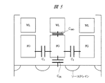
図3は、NAND型フラッシュメモリのメモリアレイ平面における、隣接フローティングゲート間の寄生容量カップリングを説明するための図である。 FIG. 3 is a diagram for explaining parasitic capacitance coupling between adjacent floating gates in the memory array plane of the NAND flash memory.
NAND型フラッシュメモリのメモリアレイにおいては、多結晶シリコンのワード線WLがX方向に走り、メモリセルの拡散層ソース、ドレインおよびチャネルであるビット線BLがY方向に走る。WLとBLの交点部分のWL下に各メモリセルの多結晶シリコンのフローティングゲートFGが形成される。 In the memory array of the NAND flash memory, the word line WL of polycrystalline silicon runs in the X direction, and the bit line BL which is the diffusion layer source, drain and channel of the memory cell runs in the Y direction. A polycrystalline silicon floating gate FG of each memory cell is formed under WL at the intersection of WL and BL.
あるメモリセルのFGに着目した場合、WL方向の両隣、BL方向の両隣、および斜め方向に隣接するメモリセルのFGが存在する。図3のように、WL<n>とBLO<n>の交点のメモリセルに着目すると、着目メモリセルのFGと、これら隣接メモリセルのFGとの間には、WL方向にはCX、BL方向にはCY、斜め方向にはCXYの寄生容量が存在する。 When attention is paid to the FG of a certain memory cell, there are FGs of memory cells adjacent to each other in the WL direction, adjacent to the BL direction, and obliquely. As shown in FIG. 3, when attention is paid to the memory cell at the intersection of WL <n> and BL O <n>, and FG of interest memory cell, between the FG of adjacent memory cells, the WL direction C X , the BL direction C Y, parasitic capacitance of C XY is present in an oblique direction.
FGはフローティングの高インピーダンスノードであるため、着目メモリセルに隣接するいずれかのメモリセルが書込まれて隣接メモリセルのFG電位が低下した場合、WL方向隣接FG間寄生容量CX、BL方向隣接FG間寄生容量CY、斜め方向隣接FG間寄生容量CXYを介して着目メモリセルのFG電位も低下する。すなわち、隣接メモリセルが書込まれてVthが上昇した場合は、着目メモリセルのVthも上昇することになる。これを近接効果と呼ぶ。 Since FG is a floating high impedance node, when any of the memory cells adjacent to the memory cell of interest is written and the FG potential of the adjacent memory cell decreases, parasitic capacitance C X between adjacent FGs in the WL direction, BL direction The FG potential of the memory cell of interest also decreases via the adjacent FG parasitic capacitance C Y and the diagonally adjacent FG parasitic capacitance C XY . That is, when adjacent memory cells are written and Vth rises, Vth of the memory cell of interest also rises. This is called a proximity effect.
図4は、NAND型フラッシュメモリのワード線方向のメモリアレイ断面における、隣接フローティングゲート間の寄生容量カップリングを説明するための図である。 FIG. 4 is a diagram for explaining the parasitic capacitance coupling between adjacent floating gates in the memory array cross section in the word line direction of the NAND flash memory.
NAND型フラッシュメモリのメモリアレイにおいては、図4のように多結晶シリコンのワード線WLの下に多結晶シリコンのFGが形成される。WL電位を上昇させたときのFG電位上昇/WL電位上昇の電圧比は、図4において寄生容量であるCXを無視すれば、CONO/(COX+CONO)の容量カップリング比で決まる。CONOはWL−FG間カップリング容量、COXは酸化膜容量を示す。書込み時にはWLに高電圧を印加してFNトンネリング書込みを行うが、FNトンネルの確率はFGとチャネル間の電界で決まるため、一定の書込み時WL電位で高いFG電位を得るためには、容量カップリング比CONO/(COX+CONO)を大きくとる必要がある。 In the memory array of the NAND flash memory, a polycrystalline silicon FG is formed under a polycrystalline silicon word line WL as shown in FIG. The voltage ratio of the FG potential rise / WL potential rise when the WL potential is raised is determined by the capacitance coupling ratio of C ONO / (C OX + C ONO ) if C X which is a parasitic capacitance is ignored in FIG. . C ONO represents a WL-FG coupling capacitance, and C OX represents an oxide film capacitance. FN tunneling writing is performed by applying a high voltage to WL at the time of writing, but since the probability of FN tunneling is determined by the electric field between FG and the channel, in order to obtain a high FG potential at a constant WL potential, a capacitance cup It is necessary to increase the ring ratio C ONO / (C OX + C ONO ).
図1のページ割付に従い、ページ0、ページ1、…、ページ63の順に書込みを行う場合、ページ0を書込んでからページ1を書込むことになる。ここで、隣接FG間の寄生容量CXを考慮した場合、ページ1の書込みによりページ1に属するメモリセルのVthが一律にΔVthaだけ上昇すると仮定すると、ページ0に属する着目メモリセルのVthは両側隣接メモリセルの近接効果の影響を受けて、ΔVtha×2CX/Ctotalだけ変動してしまう。CtotalはCOX、CONOを含む着目メモリセルFGに付くすべての容量である。
When writing is performed in the order of
このように、近接効果の程度は寄生容量カップリング係数CX/Ctotalの大きさによって決まる。プロセス微細化にともない隣接メモリセル間の距離も近くなってくるため、大容量化が進むと近接効果の程度も大きくなる。 As described above, the degree of the proximity effect is determined by the magnitude of the parasitic capacitance coupling coefficient C X / C total . As the process becomes finer, the distance between adjacent memory cells becomes closer, so the degree of proximity effect increases as the capacity increases.
図5は、NAND型フラッシュメモリのビット線方向のメモリアレイ断面における、隣接フローティングゲート間の寄生容量カップリングを説明するための図である。 FIG. 5 is a diagram for explaining the parasitic capacitance coupling between adjacent floating gates in the memory array cross section in the bit line direction of the NAND flash memory.
図4におけるCXと同様、BL方向についても隣接FG間に寄生容量CYが存在する。 As with C X in FIG. 4, there is a parasitic capacitance C Y between adjacent FG for BL direction.
図1のページ割付に従い、ページ0、ページ1、…、ページ63の順に書込みを行う場合、ページ0、ページ2を書込んでからからページ4、ページ6を書込むことになる。ここで、隣接FG間の寄生容量CYを考慮した場合、ページ6の書込みによりページ6に属するメモリセルのVthが一律にΔVthaだけ上昇すると仮定すると、ページ0、ページ2に属する着目メモリセルのVthは片側隣接メモリセルの近接効果の影響を受けて、ΔVtha×CY/Ctotalだけ変動してしまう。CtotalはCOX、CONOを含む着目メモリセルFGに付くすべての容量である。
When writing is performed in the order of
図4と同様、このような近接効果の程度は寄生容量カップリング係数CY/Ctotalの大きさによって決まる。プロセス微細化にともない隣接メモリセル間の距離も近くなってくるため、大容量化が進むと近接効果の程度も大きくなる。 As in FIG. 4, the degree of such proximity effect is determined by the magnitude of the parasitic capacitance coupling coefficient C Y / C total . As the process becomes finer, the distance between adjacent memory cells becomes closer, so the degree of proximity effect increases as the capacity increases.
なお、図4、図5では、それぞれWL方向、BL方向の隣接FG間寄生容量による近接効果について説明したが、図3に示すように斜め方向にもCXYの寄生容量が付く。プロセス世代が進むにつれて、CX、CY、CXYのいずれも大きくなる。 Incidentally, FIG. 4, FIG. 5, WL directions has been described proximity effect due BL direction of adjacent FG parasitic capacitance, the parasitic capacitance of C XY stick in a diagonal direction as shown in FIG. As the process generation progresses, all of C X , C Y , and C XY increase.
図6は、NAND型フラッシュメモリにおける、近接効果による閾値電圧変動を説明するための図である。 FIG. 6 is a diagram for explaining threshold voltage fluctuations due to the proximity effect in the NAND flash memory.
図3、図4および図5で示したような隣接FG間寄生容量により、あるページに含まれるメモリセルに着目した場合、着目ページが書込まれた後で隣接メモリセルを含むページが書込まれると、着目ページに属するメモリセルのVthが近接効果により上昇する。 When attention is paid to the memory cell included in a certain page due to the parasitic capacitance between adjacent FGs as shown in FIGS. 3, 4 and 5, the page including the adjacent memory cell is written after the target page is written. As a result, the Vth of the memory cell belonging to the page of interest rises due to the proximity effect.
これをVth分布として捉えると、図6のようになる。ある書込みベリファイレベルに対して書込みを行う場合、着目する書込み対象ページ内の全メモリセルのVthが書込みベリファイレベル以上になるまで書込みを繰り返し、すべてのメモリセルが書込みベリファイレベルに達した時点で書込み終了となる。このときの書込み直後の着目ページのメモリセルのVth分布は図6の点線の分布であるとする。 When this is regarded as a Vth distribution, it is as shown in FIG. When writing to a certain write verify level, the write is repeated until Vth of all memory cells in the target write target page becomes equal to or higher than the write verify level, and writing is performed when all the memory cells reach the write verify level. End. At this time, it is assumed that the Vth distribution of the memory cell of the page of interest immediately after writing is the distribution of the dotted line in FIG.
次に、着目ページ内メモリセルに隣接するメモリセルを含むページを書込むと、着目ページ内メモリセルは近接効果の影響を受けてVthが上昇する。近接効果によるVthシフト量は隣接メモリセルのVthシフト量×寄生容量カップリング係数で決まるため、隣接メモリセルのデータに依存する。このため、着目ページ内のメモリセルには、隣接メモリセルのデータパターンによって、近接効果の影響を大きく受けるメモリセルとほとんど影響を受けないメモリセルが存在することになる。 Next, when a page including a memory cell adjacent to the memory cell in the page of interest is written, the memory cell in the page of interest is affected by the proximity effect and Vth rises. Since the Vth shift amount due to the proximity effect is determined by the Vth shift amount of the adjacent memory cell × parasitic capacitance coupling coefficient, it depends on the data of the adjacent memory cell. For this reason, the memory cells in the page of interest include memory cells that are greatly affected by the proximity effect and memory cells that are hardly affected by the data pattern of the adjacent memory cell.
よって、図6に示すように着目ページのメモリセルのVth分布は近接効果の影響を受けるとVthが高い側に広がることになる。 Therefore, as shown in FIG. 6, the Vth distribution of the memory cell of the page of interest spreads to the higher Vth side when affected by the proximity effect.
多値NAND型フラッシュメモリにおいては、図2のようにVth分布を4値に書き分けるために、2値NAND型フラッシュメモリに対して各Vth分布の取れる範囲は狭くなる。また、FGに注入した電子は酸化膜を通して徐々に抜けていくため、Vth分布は時間とともに変動する。このため、多値NAND型フラッシュメモリではデータ保持時間などの信頼性は2値NAND型フラッシュメモリに対して劣る。 In the multi-level NAND flash memory, since the Vth distribution is written into four values as shown in FIG. 2, the range in which each Vth distribution can be taken becomes narrower than the binary NAND flash memory. Further, since electrons injected into the FG gradually escape through the oxide film, the Vth distribution varies with time. For this reason, in the multi-level NAND flash memory, the reliability such as the data retention time is inferior to the binary NAND flash memory.
近接効果によるVth分布の広がりで、4値の書込み後の各Vth分布間が近づいてしまうため、今後、プロセス微細化で近接効果が顕著になるにつれ、ますます信頼性が確保できなくなってくる。書換え回数が増えると酸化膜が劣化するため、書込み後の酸化膜を通してのFGからの電子流出も顕著になり、書換え回数とデータ保持時間を確保することが今後ますます困難になる。 Since the Vth distribution spreads due to the proximity effect, the Vth distributions after the four-value writing approach each other. As the proximity effect becomes more prominent in the process miniaturization in the future, the reliability cannot be secured. As the number of rewrites increases, the oxide film deteriorates, so that the outflow of electrons from the FG through the oxide film after writing becomes significant, and it becomes increasingly difficult to secure the number of rewrites and the data retention time in the future.
そこで、本発明の各実施の形態では、これらの課題に対して、以下に説明する構成および制御方法により解決している。 Therefore, in each embodiment of the present invention, these problems are solved by the configuration and control method described below.
<本発明の実施の形態1>
本発明の実施の形態1を、図7〜図11を用いて説明する。
<
A first embodiment of the present invention will be described with reference to FIGS.
図7は、実施の形態1のNAND型フラッシュメモリシステムの構成を説明するための図である。 FIG. 7 is a diagram for explaining the configuration of the NAND flash memory system according to the first embodiment.
NAND型フラッシュメモリシステムは、複数のメモリセルを有するNAND型フラッシュメモリチップ1と、このNAND型フラッシュメモリチップ1の各メモリセルへの書込みを制御するメモリコントローラ2から構成される。なお、NAND型フラッシュメモリチップ1は、単にフラッシュメモリチップ1とも記述する。
The NAND flash memory system includes a NAND
NAND型フラッシュメモリチップ1は、各ワード線WLと各ビット線BLとの交点に配置された複数のメモリセルMCなどからなるメモリアレイ11(詳細は図9)と、各ワード線WLなどを駆動するXデコーダ12と、各ビット線BLを駆動してデータの書込みおよび読出しなどを行うセンス回路/書込みデータバッファ13と、寄生容量カップリング係数の実測値などを書込んでおく管理領域14などから構成される。
The NAND
メモリコントローラ2は、アドレスおよび書込みユーザデータなどを格納するワークRAM21と、データ変換処理プログラムなどを格納するコードROM22と、データ変換処理プログラムなどに基づいて処理を実行するCPU23などから構成される。
The
以上のように構成されるNAND型フラッシュメモリシステムでは、メモリコントローラ2にてユーザデータを受け取り、ワークRAM21に格納する。従来のNAND型フラッシュメモリではページ(=1/4WL)単位で書込みを行うが、本発明では隣接WL、隣接BLおよび斜め隣接メモリセル間の近接効果のいずれも低減するため、ページ単位ではなく、複数WL、複数BLからなるブロックを単位として書込みを行う。このため、ワークRAM21内に逐次ユーザデータを格納し、ユーザデータの容量が1ブロックの容量に達した時点で近接効果低減のためのデータ変換を開始する。
In the NAND flash memory system configured as described above, the user data is received by the
1ブロック分のユーザデータがワークRAM21に格納された後、CPU23は近接効果低減のためのデータの変換を開始する。特に制限されないが、隣接FG間の寄生容量カップリング係数は、隣接WL間、隣接BL間、斜め隣接メモリセル間のそれぞれの値がフラッシュメモリチップ1のテスト時に測定され、その値がフラッシュメモリチップ1内の管理領域14に書込まれており、フラッシュメモリシステムの電源投入時にフラッシュメモリチップ1から読出されてメモリコントローラ2内のワークRAM21あるいはCPU23内のレジスタに書込まれ、高速に読出せるようにしておく。
After the user data for one block is stored in the
1ブロックのユーザデータと寄生容量カップリング係数をもとに、CPU23はデータ変換を行う。近接効果を与えるメモリセルを加害メモリセル、近接効果を受けるメモリセルを被害メモリセルとすると、被害メモリセルの近接効果によるVth上昇は、
被害メモリセルΔVth=寄生容量カップリング係数×加害メモリセルΔVth
・・・式(1)
で表せるため、ブロック全体にわたって書込まれるページ順にΔVthを計算してブロック書込み終了後の近接効果を受けた状態の各メモリセルVthを予測計算できる。
The
Damaged memory cell ΔVth = parasitic capacitance coupling coefficient × harmful memory cell ΔVth
... Formula (1)
Therefore, ΔVth can be calculated in the order of pages written over the entire block, and each memory cell Vth in a state of receiving the proximity effect after completion of block writing can be predicted.
近接効果を受けた状態での書込み終了後のVthを予測できるので、近接効果を受けた場合にちょうど目標と一致するようなVthを計算することが可能である。すなわち、近接効果を受けてVthが上昇する分だけ予め低いVthに書込むことが可能である。 Since it is possible to predict Vth after completion of writing in a state where the proximity effect is received, it is possible to calculate Vth that exactly matches the target when the proximity effect is received. That is, it is possible to write to a lower Vth in advance as Vth rises due to the proximity effect.
あるメモリセルを4値でデータ‘00’に相当する3.0VのVthに書込みたいとする。実際は2.8Vに書込めば、ブロック書込み終了後にちょうど3.0Vになると計算できたとする。フラッシュメモリチップ1は、各メモリセルがlog2nビットの情報を記憶する場合、n値読出しでありながらm値に書き分けることが可能なように構成しておく。ここで、m>nである。例として‘11’、‘10’、‘00’、‘01’の4値読出しで16値書込みの構成とする。‘0000’に書込むためのベリファイレベルが3.0Vであり、‘0001’に書込むためのベリファイレベルが2.9Vであり、‘0010’に書込むためのベリファイレベルが2.8Vであり、‘0011’に書込むためのベリファイレベルが2.7Vであるような回路をNAND型フラッシュメモリチップ1に実現しておく。読出し時に‘00’と読出したいので、書込み後のVthは3.0Vとしたい。メモリコントローラ2内での計算により、ベリファイレベル2.8Vに書込めばブロック書込み終了後に3.0VのVthとなることが分かっているから、メモリコントローラ2が受けるユーザデータ‘00’はメモリコントローラ2内で‘0010’に変換する。
It is assumed that a certain memory cell is written in Vth of 3.0 V corresponding to data “00” in four values. Actually, if it is written to 2.8V, it can be calculated that it becomes exactly 3.0V after the block writing is completed. The
この変換処理はメモリコントローラ2内のCPU23により行う。一連の変換処理のプログラムはコードROM22に格納されており、CPU23はコードROM22から命令をフェッチしてワークRAM21の読出し、書込みを繰り返し、上記変換処理を行う。
This conversion process is performed by the
メモリコントローラ2は、変換したデータをNAND型フラッシュメモリチップ1に転送し、フラッシュメモリチップ1は通常のページ単位の書込みを繰り返し、16値のブロック書込みを行う。上記の‘00’として読出したいメモリセルは‘0010’のデータとして2.8VのVthに書込まれるが、その後、近接効果の被害を受け、ブロック全体の書込み終了後は3.0VのVthとなる。
The
また、読出し時は通常の動作により4値として読出すため、読出し速度の低下は無い。以上のように、近接効果によるΔVth計算、ブロック書込み終了時に目標のVthに落ち着くためのベリファイレベル計算、データの変換処理により近接効果低減が可能となる。 Further, since reading is performed as four values by a normal operation at the time of reading, there is no decrease in reading speed. As described above, the proximity effect can be reduced by the ΔVth calculation based on the proximity effect, the verify level calculation for reaching the target Vth at the end of block writing, and the data conversion process.
図8は、実施の形態1のNAND型フラッシュメモリシステムにおいて、書込み動作を説明するための図である。(a)は通常の書込み動作を示し、(b)は本実施の形態の書込み動作を示す。 FIG. 8 is a diagram for explaining a write operation in the NAND flash memory system according to the first embodiment. (A) shows a normal write operation, and (b) shows a write operation of the present embodiment.
通常の4値NAND型フラッシュメモリチップの書込み動作では、図8(a)のように、消去状態からベリファイレベル1,2,3に向かって書込みが行われ、どのメモリセルも書込み直後はベリファイレベルに近いVthにあるものの、書込みが進むにつれ、近接効果の影響を受けて高Vth側に分布が広がってしまう。
In the write operation of a normal four-value NAND flash memory chip, as shown in FIG. 8A, writing is performed from the erased state toward the verify
これに対し、本実施の形態1の書込み動作では、図8(b)のように、データパターンに応じてA部の部分に示すように最終的に書込みたいVthレベルよりも低い電圧にベリファイレベル(図8(b)では細線による点線で図示した3レベルの例)が設定されるメモリセルが存在する。これらA部の部分に存在するメモリセルも、近接効果の影響を受け、最終的にはA部の部分より高Vth側に移動し、狭いVth分布を形成することが可能である。 On the other hand, in the write operation of the first embodiment, as shown in FIG. 8B, the verify level is set to a voltage lower than the Vth level to be finally written as shown in the portion A according to the data pattern. There is a memory cell in which (a three-level example illustrated by a thin dotted line in FIG. 8B) is set. The memory cells existing in the A portion are also affected by the proximity effect, and finally move to a higher Vth side than the A portion, thereby forming a narrow Vth distribution.
これにより、図8に示すように、通常の書込み動作に比べて本実施の形態1の書込み動作では、各Vth分布の裾と各読出しレベル間のVthウィンドウマージンも広く取れるため、データ保持時間、書換え耐性のような信頼性を損なうことなく、微細化が可能となる。または、4値以上の8値、16値といった多値化による大容量化が可能となる。 As a result, as shown in FIG. 8, in the write operation of the first embodiment, the Vth window margin between each Vth distribution and each read level can be widened in comparison with the normal write operation. Miniaturization is possible without impairing reliability such as rewrite resistance. Alternatively, it is possible to increase the capacity by multi-values such as 8-values and 16-values greater than 4 values.
図9は、実施の形態1のNAND型フラッシュメモリシステムにおいて、ページ割付を説明するための図である。 FIG. 9 is a diagram for explaining page allocation in the NAND flash memory system according to the first embodiment.
本実施の形態1においては、データパターン依存の近接効果を予測するため、あるメモリセルに着目した場合に隣接WL、隣接BL、斜め隣接メモリセルのデータが既知である必要がある。そのため、書込みは複数WL、複数BLを含む消去ブロックの単位で行う必要がある。 In the first embodiment, in order to predict a data pattern-dependent proximity effect, when attention is paid to a certain memory cell, the data of adjacent WL, adjacent BL, and diagonally adjacent memory cells must be known. Therefore, it is necessary to perform writing in units of erase blocks including a plurality of WLs and a plurality of BLs.
ただし、フラッシュメモリチップ内では偶数BLと奇数BLでベリファイに必要なセンスアンプが共有されており、またアレイ構成上、複数WLのいくつかに書込みを行い、その他のWLは書込みを阻止するということは不可能であるため、ブロック全体を同時に書込むことはできない。よって、従来通り、ブロックよりも小さなサイズのページを一度に書込む単位とし、ページ書込みを繰り返すことで全消去ブロックを書込む必要がある。 However, in the flash memory chip, even-numbered BL and odd-numbered BL share a sense amplifier necessary for verification, and in the array configuration, some WLs are written and other WLs block writing. Cannot be written at the same time. Therefore, as usual, it is necessary to write all erase blocks by repeating page writing with a page having a size smaller than the block written at a time.
また、本実施の形態1では、図7の説明で述べたとおり、‘00’データから‘0010’データというようにデータを変換して、読出しよりも書込み時のVth分解能を上げる必要があるため、上位ビットと下位ビットを別のページに割り付けることはせず、同じページに割り付ける方が実施が容易である。このため、図9のように、1ページ=1/2WLで上位ビットと下位ビットは同一ページというページ割付(ページ0〜31)が好適である。すなわち、同一ワード線WLに接続されるメモリセルMCのうち偶数ビット線BLE/奇数ビット線BLOは別ページとするが、同一メモリセルMC内で多値の上位ビットと下位ビットを同一ページとする。
Further, in the first embodiment, as described in the explanation of FIG. 7, it is necessary to convert data from “00” data to “0010” data to increase the Vth resolution at the time of writing rather than reading. It is easier to implement without assigning the upper bit and the lower bit to different pages and assigning them to the same page. Therefore, as shown in FIG. 9, page allocation (
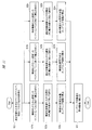
図10は、実施の形態1のNAND型フラッシュメモリシステムにおいて、メモリコントローラ内でのデータ変換処理方法を説明するためのフローチャートである。 FIG. 10 is a flowchart for explaining a data conversion processing method in the memory controller in the NAND flash memory system according to the first embodiment.
図9のページ0から順に最終ページであるページ31まで書込むにあたって、ページ<n>に属するメモリセルVthは、ページ<n+1>、ページ<n+2>、ページ<n+2>から被害を受ける可能性がある。前述した式(1)により近接効果による被害メモリセルのΔVthが計算でき、この式に従い最初に書込まれるページ0から順にページ31まで、ブロック書込み終了後の全メモリセルのVthを予測計算する(S1)。
When writing from
図9で示すように、ページ31は最後に書込まれるページであるため、近接効果による被害を受けない。このため、ページ31に属する全メモリセルのベリファイレベルはデータから直ちに確定する(S2)。このように最後に書込まれるページから遡って、順に若いページへとブロック書込み後に近接効果の影響がキャンセルされるようなデータへの変換を行っていく。
As shown in FIG. 9, the
まず、ページ30のデータ変換開始にあたって(S3)、このページ30はページ31の前に書かれるページであるため、ページ31から被害を受ける。上記の予測計算において、ページ30の中でアドレスが最も若いメモリセルのベリファイレベルとして、例えば最も低い消去レベルのVthを与え(S4)、ブロック内全メモリセルの書込み終了後Vthを再計算する(S5)。
First, when data conversion of the
ページ30のアドレス最若メモリセルのブロック書込み後のVth予測計算値が、最終的に目標とするVthレベルに達していなければ(S6−No)、ベリファイレベル値を設定幅だけインクリメントし(S7)、再度ブロック内の全メモリセルのブロック書込み後Vthを予測計算する。予測計算値が目標値を上回るまでこれを繰り返し、目標値を上回った時点、すなわちブロック書込み後の対象メモリセルVthが目標値に近くなった時点で(S6−Yes)、対象メモリセルについて反復計算を終了する。
If the Vth prediction calculation value after block writing of the address youngest memory cell of
この後、対象メモリセルのベリファイレベルから、データ論理値の変換を行う(S8)。例えば、最終的にデータ‘00’と読出すためにVthを3.0Vに書込みたいが、そのためには近接効果を受ける前では2.8Vとする必要があり、これは書込みデータとしては‘0010’に相当するという場合、対象メモリセルに書込むデータを‘00’から‘0010’に変換する。 Thereafter, the data logical value is converted from the verify level of the target memory cell (S8). For example, Vth should be written to 3.0 V in order to finally read data “00”. For this purpose, it is necessary to set Vth to 2.8 V before receiving the proximity effect. In the case of “corresponding to“, ”data to be written to the target memory cell is converted from“ 00 ”to“ 0010 ”.
仮に同じくデータ‘00’と読出すためにVthを3.0Vに書込みたいが、そのためには近接効果を受ける前で2.9Vとする必要があり、これは書込みデータとしては‘0001’に相当するという場合、対象メモリセルに書込むデータを‘00’から‘0001’に変換する。このように同じデータを書込む場合でも、周囲隣接メモリセルのデータパターンにより近接効果の程度が異なるため、変換後のデ−タは異なる。 Similarly, Vth is to be written to 3.0 V in order to read data “00”, but for this purpose, it is necessary to set it to 2.9 V before receiving the proximity effect, which corresponds to “0001” as write data. In this case, data to be written to the target memory cell is converted from “00” to “0001”. Even when the same data is written in this way, the degree of the proximity effect differs depending on the data pattern of the neighboring memory cells, so that the data after conversion is different.
このように、対象メモリセルについてのデータ変換を行った後、全アドレスについてベリファイ値計算が終了するまで(S9)、計算対象のアドレスをインクリメントし(S10)、ページ30内のすべてのメモリセルについて変換を行う。ページ30の変換が終了したら、次はページ29というように、全ページについてベリファイ値計算が終了するまで(S11)、対象ページをデクリメントし(S12)、後で書込まれるページから遡って、順番にメモリセル毎にデータ変換を行う。
Thus, after the data conversion for the target memory cell is performed, the calculation target address is incremented (S10) until the verify value calculation is completed for all the addresses (S10), and all the memory cells in the
以上のように、着目メモリセルのベリファイレベルをインクリメントしながらベリファイレベル最適値を探索することで、汎用的な計算アルゴリズムを提供することができる。例えば図9において、ページ28を書いた時点でページ31は斜め方向の近接効果を受ける。ページ29を書いた時点でページ31は隣接WL間の近接効果を受ける。ページ30を書いた時点でもページ31は隣接BL間の近接効果を受ける。これにより、ページ31の書込みによりページ30が被害を受ける以前にページ31も被害を受けて、ページ31に属するメモリセルVthは消去レベルから上昇している可能性がある。
As described above, a general-purpose calculation algorithm can be provided by searching for the verify level optimum value while incrementing the verify level of the memory cell of interest. For example, in FIG. 9, when the
このため、ページ31を書込んでページ30が被害を受ける場合、ページ31のΔVth(加害)は消去レベルからの変動ではなく、すでに被害を受けて上昇しているVthからの変動となる。このような効果も考慮すると、単純にページ31から遡って、前述した式(1)の逆関数を用いてページ0まで変換していく方法では誤差が大きい。このため、図10のように着目メモリセルのベリファイレベルを更新してブロック全体にわたり全メモリセルのVthをその都度計算し、探索的に最適ベリファイレベルを求める方法が簡便であり高精度である。また、フラッシュメモリ以外のメモリにおいて、近接効果の機構は式で表すことができるが、この逆関数を解析的に求めることが困難という場合においても簡便に計算を行うことができる。
For this reason, when
データ変換の計算はワークRAM21を用いて行われ、結果はワークRAM21上に格納されている。データ変換が終了したら、ページ0から順にフラッシュメモリチップ1へとデータを転送し、書込みを開始する。データ転送と書込みは同時に行えるため、ブロックの変換後データすべてを転送してからフラッシュメモリチップ1内で書込みを開始する必要はない。すなわち、ページ0の書込みと同時にページ1の変換後データの転送を行うことで、フラッシュメモリチップ1内の書込みデータバッファの容量を削減し、書込み時間を短縮することができる。
Data conversion calculation is performed using the
図11は、実施の形態1のNAND型フラッシュメモリシステムにおいて、寄生容量カップリング係数を実測する方法を説明するためのフローチャートである。 FIG. 11 is a flowchart for explaining a method of actually measuring the parasitic capacitance coupling coefficient in the NAND flash memory system according to the first embodiment.
データ変換の計算に用いる寄生容量カップリング係数は、製造時の寸法バラツキにより変動する。このため、テスト工程あるいは出荷後のフィールドにおいて、ロット、ウェハ、チップ、バンクあるいはブロック別に実測値を測定し、この値を用いて計算を行うことでバラツキの影響下でも高精度に近接効果の影響を低減できる。ブロック毎に実測値を測定すればブロック間バラツキの影響を低減できるので最も効果的であるが、テスト時間や測定値を書込んでおく管理領域増加のコスト要因と補正対象の粒度とはトレードオフの関係となる。 The parasitic capacitance coupling coefficient used for the data conversion calculation varies depending on the dimensional variation at the time of manufacture. For this reason, in the test process or post-shipment field, measured values are measured for each lot, wafer, chip, bank or block, and calculation is performed using these values. Can be reduced. Measuring the measured value for each block is the most effective because it can reduce the influence of variation between blocks, but there is a trade-off between the cost factor for increasing the management area in which the test time and measured values are written and the granularity of the correction target It becomes the relationship.
図11のフローに示すように、寄生容量カップリング係数は、隣接WL間、隣接BL間、斜め隣接メモリセル間で値が異なるため、それぞれについて別々に測定する必要がある。 As shown in the flow of FIG. 11, the parasitic capacitance coupling coefficient has a different value between adjacent WLs, between adjacent BLs, and between diagonally adjacent memory cells, and therefore needs to be measured separately for each.
測定のフローとしては、まず測定対象のメモリセルを含むブロック全体を消去(消去レベルにVth分布狭帯化)し(S21)、測定対象のメモリセルに対し、隣接メモリセル(隣接WL間、隣接BL間、斜め隣接メモリセル間)を既定のベリファイレベルに向けて書込む(S22a,S22b,S22c)。その後、測定対象のメモリセルのVthを測定する(S23a,S23b,S23c)。これは、WL電圧を細かい電圧ステップでインクリメントし、センスアンプ出力が反転するWL電圧を探すことで実施できる。近接効果を与える加害メモリセルのVth変動量は、ベリファイレベルと消去レベルの差より既知であるから、前述した式(1)より寄生容量カップリング係数を求める(S24a,S24b,S24c)。そして、寄生容量カップリング係数値を管理領域14に書込む(S25)。 As a measurement flow, first, the entire block including the memory cell to be measured is erased (Vth distribution narrowing to the erase level) (S21), and the adjacent memory cell (between adjacent WL, adjacent to the measurement target memory cell) Write between BL and diagonally adjacent memory cells toward a predetermined verify level (S22a, S22b, S22c). Thereafter, Vth of the memory cell to be measured is measured (S23a, S23b, S23c). This can be done by incrementing the WL voltage in fine voltage steps and looking for the WL voltage at which the sense amplifier output is inverted. Since the Vth variation amount of the harmful memory cell giving the proximity effect is known from the difference between the verify level and the erase level, the parasitic capacitance coupling coefficient is obtained from the above-described equation (1) (S24a, S24b, S24c). Then, the parasitic capacitance coupling coefficient value is written in the management area 14 (S25).
以上説明したように、本実施の形態1のNAND型フラッシュメモリシステムによれば、NAND型フラッシュメモリチップ1と、このNAND型フラッシュメモリチップ1の各メモリセルへの書込みを制御するメモリコントローラ2とを有することで、以下のような効果を得ることができる。
As described above, according to the NAND flash memory system of the first embodiment, the NAND
(1)フラッシュメモリチップ1に書込む前に近接効果によるVth上昇量をメモリセル毎に計算し、近接効果の影響下で消去ブロック全体が書込まれた後に各メモリセルが目標とするVthに落ち着くようにメモリセル毎に予め補正をかけたベリファイレベルに対して書込むため、デバイス微細化による近接効果の影響を低減して狭帯化したVth分布を形成できる。このため、多値フラッシュメモリにおいても各論理レベル間のVthウィンドウマージン、すなわち信頼性が確保でき、大容量を実現するために今後も微細化を進めることが可能となる。
(1) The amount of increase in Vth due to the proximity effect is calculated for each memory cell before writing to the
(2)従来のページ単位ではなく、複数WL、複数BLから成るブロック全体についてデータを書込むため、隣接WL間、隣接BL間、斜め隣接メモリセル間のいずれの近接効果も低減可能となる。 (2) Since data is written for the entire block composed of a plurality of WLs and a plurality of BLs instead of the conventional page unit, any proximity effect between adjacent WLs, between adjacent BLs, and between diagonally adjacent memory cells can be reduced.
(3)寄生容量カップリング係数として、予め決めた設定値ではなく実測値を用いて補正計算を行うため、製造バラツキに強い近接効果低減が可能となる。 (3) Since the correction calculation is performed using the actually measured value instead of the predetermined set value as the parasitic capacitance coupling coefficient, it is possible to reduce the proximity effect that is strong against manufacturing variations.
(4)書込み対象ブロックについて、消去レベルから書込みを始めるため、前記特許文献2の追加書込みに比べて初期電圧設定が容易である。
(4) Since writing is started from the erase level for the block to be written, initial voltage setting is easier compared to the additional writing described in
(5)反復計算により数値計算を行い、探索的にユーザデータパターンを補正後データパターンに変換するので、近接効果の機構を数式で表現できさえすればよく、近接効果を表現した数式の逆関数を求めるといった手続きが不要となる。例えば、フラッシュメモリ以外のメモリで近接効果の機構が複雑な数式で表現されるような場合にも適用し易い。 (5) Since numerical calculation is performed by iterative calculation and the user data pattern is converted into a corrected data pattern in an exploratory manner, it is only necessary to express the mechanism of the proximity effect by a mathematical expression, and an inverse function of the mathematical expression expressing the proximity effect. The procedure of requesting is no longer necessary. For example, it can be easily applied to a case where the proximity effect mechanism is expressed by a complicated mathematical expression in a memory other than a flash memory.
(6)近接効果の影響を低減でき、Vth分布を狭帯化できるため、8値、16値、32値/メモリセルといった多値化推進によるメモリ大容量化が可能となる。 (6) Since the influence of the proximity effect can be reduced and the Vth distribution can be narrowed, it is possible to increase the memory capacity by promoting multi-values such as 8-value, 16-value, and 32-value / memory cells.
(7)フラッシュメモリチップ1としては、n値読出し、m値書込み(ただしm>n)が実現でき、読出しよりも書込みが高分解能であればよく、補正変換計算は汎用マイコン(CPU23)+DRAM(ワークRAM21)のメモリコントローラ2で行い、補正変換後データパターンをフラッシュメモリチップ1に転送するというシステム構成が可能である。よって、専用コントローラチップを用いずとも低コストなフラッシュメモリシステムが実現可能となる。
(7) As the
<本発明の実施の形態2>
本発明の実施の形態2を、図12を用いて説明する。
<
A second embodiment of the present invention will be described with reference to FIG.
図12は、実施の形態2のNAND型フラッシュメモリシステムにおいて、シールド領域確保による書込み単位の小容量化を説明するための図である。 FIG. 12 is a diagram for explaining a reduction in capacity of a write unit by securing a shield area in the NAND flash memory system according to the second embodiment.
前記実施の形態1に対応する図9のブロックは、16WLで32ページから成る。実際は、同時に書込む単位としては1ページ=1/2WL毎であり、ページ書込みを繰り返すことでブロック全体を書込むが、隣接メモリセルのデータを考慮して補正をかけるために、1ブロックのデータをまとめて書込む必要がある。この場合、通常のフラッシュメモリチップに対して書込み単位のサイズが大きくなってしまい、使い勝手が悪くなることが懸念される。 The block of FIG. 9 corresponding to the first embodiment is composed of 32 pages of 16 WL. Actually, the unit of simultaneous writing is 1 page = 1/2 WL every, and the entire block is written by repeating page writing. However, in order to apply correction in consideration of the data of adjacent memory cells, the data of one block Need to be written together. In this case, there is a concern that the size of the writing unit becomes larger than that of a normal flash memory chip, and the usability is deteriorated.
そこで、本実施の形態2では、図12に示すようなブロック割付とする。一つのブロックを、WL<0>からWL<6>までの7WL=14ページと、WL<9>からWL<15>までの7WL=14ページに2分割する。WL<7>はWL<6>にとって近接効果加害となり、WL<8>はWL<9>から近接効果被害を受けるため、これらは通常のメモリとして使用せず、ダミーのシールドWLとして用いる。こうすることで、書込みの単位を1ブロック=16WL=32ページから7WL=14ページに低減可能であり、使い勝手が向上する。 Therefore, in the second embodiment, the block allocation is as shown in FIG. One block is divided into 7 WL = 14 pages from WL <0> to WL <6> and 7WL = 14 pages from WL < 9> to WL <15> . Since WL <7> causes proximity effect damage to WL <6> and WL <8> suffers proximity effect damage from WL <9> , these are not used as ordinary memories but as dummy shields WL. By doing so, the unit of writing can be reduced from 1 block = 16 WL = 32 pages to 7WL = 14 pages, and usability is improved.
ただし、書込み単位境界のWLをシールドとして使用する必要があるため、書込み単位を小さくするほどシールドWLが増加して、実際にユーザが使用できるメモリ容量は減少する。 However, since it is necessary to use the WL at the write unit boundary as a shield, the shield WL increases as the write unit is reduced, and the memory capacity actually usable by the user decreases.
なお、図12では、書込み単位のサイズを一定に保つため、WL<7>およびWL<8>の2WLをシールド領域に設定しているが、WL<7>のみをシールドとして、WL<0>からWL<6>の7WL=14ページと、WL<8>からWL<15>の8WL=16ページに書込み単位を分割してもよい。または、1ブロックを偶数本ではなく奇数本のWLから成る構成とすれば、1WLをシールドとして用いつつ、同一サイズの書込み単位に2分割することが可能である。さらに、2分割に限られるものではなく、3分割以上でもよい。 In FIG. 12, for keeping the size of the write unit constant, but has set 2WL of WL <7> and WL <8> in the shield region, WL <7> only as a shield, WL <0> The write unit may be divided into 7WL = 14 pages from WL <6> to 8WL = 16 pages from WL < 8> to WL <15> . Alternatively, if one block is composed of an odd number of WLs instead of an even number, it is possible to divide into two writing units of the same size while using 1WL as a shield. Furthermore, it is not limited to two divisions and may be three or more divisions.
また、本実施の形態2においては、消去ブロックを分割した分割ブロックを書込み単位とする以外は前記実施の形態1と同様であり、この分割ブロックの全メモリセルについて、近接効果による閾値電圧の上昇量を予めデータパターンと寄生容量カップリング係数から計算し、分割ブロックの書込み終了後に目標の閾値電圧になるようにメモリセル毎に書込み時ベリファイレベルを予め調整してから書込む。この近接効果が補正された変換後データパターンを生成する際には、書込むユーザデータから書込み後の各メモリセルの閾値電圧を予測計算し、書込み時ベリファイレベルを調整しながら書込み後の閾値電圧を計算して、分割ブロックの書込み終了時の目標の閾値電圧と予測計算した書込み後の閾値電圧の差が許容範囲以内になるまで反復計算を繰り返す。また、寄生容量カップリング係数は、ロット、ウェハ、チップ、バンクあるいは分割ブロック別に実測値を測定し、この値を用いて計算を行うことで高精度に近接効果の影響が低減できる。 The second embodiment is the same as the first embodiment except that a divided block obtained by dividing an erase block is used as a write unit. For all memory cells in this divided block, the threshold voltage rises due to the proximity effect. The amount is calculated in advance from the data pattern and the parasitic capacitance coupling coefficient, and is written after the verify level at the time of writing is adjusted in advance for each memory cell so that the target threshold voltage is obtained after the writing of the divided blocks is completed. When generating the converted data pattern in which this proximity effect is corrected, the threshold voltage of each memory cell after writing is predicted from the user data to be written, and the threshold voltage after writing is adjusted while adjusting the verify level during writing. And the iterative calculation is repeated until the difference between the target threshold voltage at the end of writing in the divided block and the predicted threshold voltage after writing is within the allowable range. Further, the parasitic capacitance coupling coefficient can be measured with an actual measurement value for each lot, wafer, chip, bank, or divided block, and calculation using this value can reduce the influence of the proximity effect with high accuracy.
以上説明したように、本実施の形態2のNAND型フラッシュメモリシステムによれば、前記実施の形態1と同様に(1)〜(7)のような効果を得ることができるとともに、消去ブロックを分割して書込み単位が低減できるため、前記実施の形態1に比べて使い勝手の向上が可能となる。 As described above, according to the NAND flash memory system of the second embodiment, the effects (1) to (7) can be obtained as in the first embodiment, and the erase block is stored in the erase block. Since the writing unit can be reduced by dividing, usability can be improved as compared with the first embodiment.
以上、本発明者によってなされた発明を実施の形態に基づき具体的に説明したが、本発明は前記実施の形態に限定されるものではなく、その要旨を逸脱しない範囲で種々変更可能であることはいうまでもない。 As mentioned above, the invention made by the present inventor has been specifically described based on the embodiment. However, the present invention is not limited to the embodiment, and various modifications can be made without departing from the scope of the invention. Needless to say.
例えば、前記実施の形態においては、NAND型フラッシュメモリを例に説明したが、これに限定されるものではなく、NOR型フラッシュメモリ、相変化メモリなどについても適用可能である。NOR型フラッシュメモリについては、近接効果の機構はNAND型フラッシュメモリと同じであるが、NAND型ほどには大容量化が進んでおらず、隣接FG間の距離もNAND型よりも遠いため、現在は近接効果の問題は顕在化していない。相変化メモリについては、ジュール熱によりカルコゲナイドの結晶状態を制御し、メモリセル抵抗素子の抵抗値を変えることでデータ書換えを行うという動作原理である。今後、微細化により隣接セル間が近づいてくると、書換え時に熱が隣接セルの抵抗値を変動させると考えられる。 For example, in the above-described embodiment, the NAND flash memory has been described as an example. However, the present invention is not limited to this, and can be applied to a NOR flash memory, a phase change memory, and the like. As for the NOR type flash memory, the proximity effect mechanism is the same as that of the NAND type flash memory, but the capacity has not increased as much as the NAND type, and the distance between adjacent FGs is farther than the NAND type. The problem of proximity effect has not been revealed. The phase change memory has an operating principle in which the crystal state of chalcogenide is controlled by Joule heat and data is rewritten by changing the resistance value of the memory cell resistance element. In the future, when adjacent cells approach each other due to miniaturization, heat is considered to change the resistance value of the adjacent cells during rewriting.
本発明のフラッシュメモリシステムは、NAND型フラッシュメモリの他、NOR型フラッシュメモリ、相変化メモリなどにも適用可能であり、さらに、HDD(Hard Disk Drive)インタフェースを備えるフラッシュSSD(Solid State Drive)、SDカード、メモリースティック、USBメモリ等の汎用メモリデバイスや、フラッシュSSDから構成されるRAIDシステムおよびストレージエリアネットワーク(SAN)などに広く利用可能である。 The flash memory system of the present invention can be applied to a NOR flash memory, a phase change memory, and the like in addition to a NAND flash memory, and further, a flash SSD (Solid State Drive) having an HDD (Hard Disk Drive) interface, It can be widely used for general-purpose memory devices such as an SD card, a memory stick, and a USB memory, a RAID system including a flash SSD, and a storage area network (SAN).
1 NAND型フラッシュメモリチップ
2 メモリコントローラ
11 メモリアレイ
12 Xデコーダ
13 センス回路/書込みデータバッファ
14 管理領域
21 ワークRAM
22 コードROM
23 CPU
WL ワード線
BL ビット線
MC メモリセル
STD,STS 制御信号
CS 共通ソース線
FG フローティングゲート
DESCRIPTION OF
22 Code ROM
23 CPU
WL Word line BL Bit line MC Memory cell STD, STS Control signal CS Common source line FG Floating gate
Claims (11)
前記フラッシュメモリは、各メモリセルが2ビット以上の情報を記憶し、消去ブロックが書込み単位とされ、
前記メモリコントローラは、前記消去ブロックの全メモリセルについて、近接効果による閾値電圧の上昇量を予めデータパターンと寄生容量カップリング係数から計算し、前記消去ブロックの書込み終了後に目標の閾値電圧になるようにメモリセル毎に書込み時ベリファイレベルを予め調整してから書込む、ことを特徴とするフラッシュメモリシステム。 A flash memory having a plurality of memory cells, and a memory controller for controlling writing to each memory cell of the flash memory,
In the flash memory, each memory cell stores information of 2 bits or more, and an erase block is a write unit.
The memory controller calculates in advance the increase amount of the threshold voltage due to the proximity effect from the data pattern and the parasitic capacitance coupling coefficient for all the memory cells of the erase block so that the target threshold voltage is obtained after the erase block is written. A flash memory system, wherein a write verify level is adjusted in advance for each memory cell before writing.
前記寄生容量カップリング係数は、ロット毎、ウェハ毎、チップ毎、バンク毎、あるいは前記消去ブロック毎に実測され、この実測値が前記フラッシュメモリの管理領域に書込まれ、
前記メモリコントローラは、前記管理領域に書込まれた実測値を利用して前記近接効果の影響に対するベリファイレベル補正量を計算し、製造ばらつきに起因する前記近接効果の補正を行う、ことを特徴とするフラッシュメモリシステム。 The flash memory system according to claim 1.
The parasitic capacitance coupling coefficient is measured for each lot, for each wafer, for each chip, for each bank, or for each erase block, and this measured value is written in the management area of the flash memory.
The memory controller calculates a verification level correction amount for the influence of the proximity effect using an actual value written in the management area, and corrects the proximity effect due to manufacturing variation. Flash memory system.
前記フラッシュメモリは、各メモリセルがlog2nビットの情報を記憶し、n値の読出しで、m>nであるm値の書込みとされ、
前記メモリコントローラは、前記n値のデータパターンを前記近接効果の補正のために前記m値のデータパターンに変換し、この変換されたm値の変換後データパターンを書込む、ことを特徴とするフラッシュメモリシステム。 The flash memory system according to claim 1.
In the flash memory, each memory cell stores log 2 n-bit information, and reading of n value is writing of m value where m> n,
The memory controller converts the n-value data pattern into the m-value data pattern for correcting the proximity effect, and writes the converted m-value converted data pattern. Flash memory system.
前記メモリコントローラは、前記データパターンと前記寄生容量カップリング係数に基づいて前記近接効果の補正計算を行い、この補正計算された変換後データパターンを前記フラッシュメモリに転送する、ことを特徴とするフラッシュメモリシステム。 The flash memory system according to claim 1.
The memory controller performs a correction calculation of the proximity effect based on the data pattern and the parasitic capacitance coupling coefficient, and transfers the converted data pattern after the correction calculation to the flash memory. Memory system.
前記メモリコントローラは、前記近接効果が補正された変換後データパターンを生成する際、書込むユーザデータから書込み後の各メモリセルの閾値電圧を予測計算し、前記書込み時ベリファイレベルを調整しながら書込み後の閾値電圧を計算して、前記消去ブロックの書込み終了時の前記目標の閾値電圧と前記予測計算した書込み後の閾値電圧との差が許容範囲以内になるまで反復計算を繰り返す、ことを特徴とするフラッシュメモリシステム。 The flash memory system according to claim 1.
When generating the converted data pattern in which the proximity effect is corrected, the memory controller predicts and calculates the threshold voltage of each memory cell after writing from the user data to be written, and writes while adjusting the verify level at the time of writing. A later threshold voltage is calculated, and the iterative calculation is repeated until the difference between the target threshold voltage at the end of writing of the erase block and the predicted calculated threshold voltage is within an allowable range. And flash memory system.
前記フラッシュメモリは、各メモリセルが2ビット以上の情報を記憶し、消去ブロックを分割した分割ブロックが書込み単位とされ、分割の物理的境界に位置するメモリセルは書込みに使用せずにシールドとして使用され、
前記メモリコントローラは、前記分割ブロックの全メモリセルについて、近接効果による閾値電圧の上昇量を予めデータパターンと寄生容量カップリング係数から計算し、前記分割ブロックの書込み終了後に目標の閾値電圧になるようにメモリセル毎に書込み時ベリファイレベルを予め調整してから書込む、ことを特徴とするフラッシュメモリシステム。 A flash memory having a plurality of memory cells, and a memory controller for controlling writing to each memory cell of the flash memory,
In the flash memory, each memory cell stores information of 2 bits or more, a divided block obtained by dividing an erase block is used as a writing unit, and a memory cell located at a physical boundary of the divided is not used for writing and serves as a shield. Used,
The memory controller calculates an increase amount of a threshold voltage due to the proximity effect in advance from a data pattern and a parasitic capacitance coupling coefficient for all the memory cells of the divided block so that a target threshold voltage is obtained after the writing of the divided block is completed. A flash memory system, wherein a write verify level is adjusted in advance for each memory cell before writing.
前記寄生容量カップリング係数は、ロット毎、ウェハ毎、チップ毎、バンク毎、あるいは前記分割ブロック毎に実測され、この実測値が前記フラッシュメモリの管理領域に書込まれ、
前記メモリコントローラは、前記管理領域に書込まれた実測値を利用して前記近接効果の影響に対するベリファイレベル補正量を計算し、製造ばらつきに起因する前記近接効果の補正を行う、ことを特徴とするフラッシュメモリシステム。 The flash memory system according to claim 6.
The parasitic capacitance coupling coefficient is measured for each lot, for each wafer, for each chip, for each bank, or for each divided block, and this measured value is written in the management area of the flash memory.
The memory controller calculates a verification level correction amount for the influence of the proximity effect using an actual value written in the management area, and corrects the proximity effect due to manufacturing variation. Flash memory system.
前記フラッシュメモリは、各メモリセルがlog2nビットの情報を記憶し、n値の読出しで、m>nであるm値の書込みとされ、
前記メモリコントローラは、前記n値のデータパターンを前記近接効果の補正のために前記m値のデータパターンに変換し、この変換されたm値の変換後データパターンを書込む、ことを特徴とするフラッシュメモリシステム。 The flash memory system according to claim 6.
In the flash memory, each memory cell stores log 2 n-bit information, and reading of n value is writing of m value where m> n,
The memory controller converts the n-value data pattern into the m-value data pattern for correcting the proximity effect, and writes the converted m-value converted data pattern. Flash memory system.
前記メモリコントローラは、前記データパターンと前記寄生容量カップリング係数に基づいて前記近接効果の補正計算を行い、この補正計算された変換後データパターンを前記フラッシュメモリに転送する、ことを特徴とするフラッシュメモリシステム。 The flash memory system according to claim 6.
The memory controller performs a correction calculation of the proximity effect based on the data pattern and the parasitic capacitance coupling coefficient, and transfers the converted data pattern after the correction calculation to the flash memory. Memory system.
前記メモリコントローラは、前記近接効果が補正された変換後データパターンを生成する際、書込むユーザデータから書込み後の各メモリセルの閾値電圧を予測計算し、前記書込み時ベリファイレベルを調整しながら書込み後の閾値電圧を計算して、前記分割ブロックの書込み終了時の前記目標の閾値電圧と前記予測計算した書込み後の閾値電圧との差が許容範囲以内になるまで反復計算を繰り返す、ことを特徴とするフラッシュメモリシステム。 The flash memory system according to claim 6.
When generating the converted data pattern in which the proximity effect is corrected, the memory controller predicts and calculates the threshold voltage of each memory cell after writing from the user data to be written, and writes while adjusting the verify level at the time of writing. A later threshold voltage is calculated, and the iterative calculation is repeated until a difference between the target threshold voltage at the end of writing of the divided block and the predicted calculated threshold voltage is within an allowable range. And flash memory system.
前記フラッシュメモリは、各メモリセルがlog2nビットの情報を記憶し、n値の読出しで、m>nであるm値の書込みとされ、
前記メモリコントローラは、前記n値のデータパターンを近接効果の補正のために前記m値のデータパターンに変換し、この変換されたm値の変換後データパターンを書込む、ことを特徴とするフラッシュメモリシステム。 A flash memory having a plurality of memory cells, and a memory controller for controlling writing to each memory cell of the flash memory,
In the flash memory, each memory cell stores log 2 n-bit information, and reading of n value is writing of m value where m> n,
The memory controller converts the n-value data pattern into the m-value data pattern to correct the proximity effect, and writes the converted m-value converted data pattern. Memory system.
Priority Applications (1)
| Application Number | Priority Date | Filing Date | Title |
|---|---|---|---|
| JP2008123653A JP2009272016A (en) | 2008-05-09 | 2008-05-09 | Flash memory system |
Applications Claiming Priority (1)
| Application Number | Priority Date | Filing Date | Title |
|---|---|---|---|
| JP2008123653A JP2009272016A (en) | 2008-05-09 | 2008-05-09 | Flash memory system |
Publications (1)
| Publication Number | Publication Date |
|---|---|
| JP2009272016A true JP2009272016A (en) | 2009-11-19 |
Family
ID=41438424
Family Applications (1)
| Application Number | Title | Priority Date | Filing Date |
|---|---|---|---|
| JP2008123653A Pending JP2009272016A (en) | 2008-05-09 | 2008-05-09 | Flash memory system |
Country Status (1)
| Country | Link |
|---|---|
| JP (1) | JP2009272016A (en) |
Cited By (11)
| Publication number | Priority date | Publication date | Assignee | Title |
|---|---|---|---|---|
| KR20110038097A (en) * | 2008-07-01 | 2011-04-13 | 엘에스아이 코포레이션 | Flash memory device reading method and system |
| JP2011529241A (en) * | 2008-07-22 | 2011-12-01 | エルエスアイ コーポレーション | Method and apparatus for programming multiple program values for each signal level in flash memory |
| US8520443B2 (en) | 2010-09-22 | 2013-08-27 | Kabushiki Kaisha Toshiba | Nonvolatile semiconductor storage device and method for driving the same |
| US8537619B2 (en) | 2010-09-22 | 2013-09-17 | Kabushiki Kaisha Toshiba | Nonvolatile semiconductor storage device and method of controlling and manufacturing the same |
| KR20150043127A (en) * | 2013-10-14 | 2015-04-22 | 삼성전자주식회사 | Coding method and decoding method in memory system |
| CN104919433A (en) * | 2013-01-11 | 2015-09-16 | 英派尔科技开发有限公司 | Page allocation for flash memories |
| US9263131B2 (en) | 2011-12-02 | 2016-02-16 | Kabushiki Kaisha Toshiba | High-speed readable semiconductor storage device |
| US9859925B2 (en) | 2013-12-13 | 2018-01-02 | Empire Technology Development Llc | Low-complexity flash memory data-encoding techniques using simplified belief propagation |
| US9898361B2 (en) | 2011-01-04 | 2018-02-20 | Seagate Technology Llc | Multi-tier detection and decoding in flash memories |
| JP2020047323A (en) * | 2018-09-14 | 2020-03-26 | キオクシア株式会社 | Memory system |
| US10770148B2 (en) | 2017-09-20 | 2020-09-08 | Samsung Electronics Co., Ltd. | Nonvolatile memory device and operating method of the same |
-
2008
- 2008-05-09 JP JP2008123653A patent/JP2009272016A/en active Pending
Cited By (25)
| Publication number | Priority date | Publication date | Assignee | Title |
|---|---|---|---|---|
| KR101626631B1 (en) | 2008-07-01 | 2016-06-01 | 엘에스아이 코포레이션 | Methods and apparatus for write-side intercell interference mitigation in flash memories |
| KR20110041501A (en) * | 2008-07-01 | 2011-04-21 | 엘에스아이 코포레이션 | Flash memory device writing method and system |
| JP2011527159A (en) * | 2008-07-01 | 2011-10-20 | エルエスアイ コーポレーション | Method and apparatus for inter-cell interference mitigation using modulation coding |
| JP2011527072A (en) * | 2008-07-01 | 2011-10-20 | エルエスアイ コーポレーション | Method and apparatus for reducing interference between write side cells in flash memory |
| JP2011527071A (en) * | 2008-07-01 | 2011-10-20 | エルエスアイ コーポレーション | Method and apparatus for reducing inter-reader cell interference in flash memory |
| KR20110038097A (en) * | 2008-07-01 | 2011-04-13 | 엘에스아이 코포레이션 | Flash memory device reading method and system |
| KR101671313B1 (en) | 2008-07-01 | 2016-11-01 | 엘에스아이 코포레이션 | Methods and apparatus for read-side intercell interference mitigation in flash memories |
| JP2011529241A (en) * | 2008-07-22 | 2011-12-01 | エルエスアイ コーポレーション | Method and apparatus for programming multiple program values for each signal level in flash memory |
| US8520443B2 (en) | 2010-09-22 | 2013-08-27 | Kabushiki Kaisha Toshiba | Nonvolatile semiconductor storage device and method for driving the same |
| US8537619B2 (en) | 2010-09-22 | 2013-09-17 | Kabushiki Kaisha Toshiba | Nonvolatile semiconductor storage device and method of controlling and manufacturing the same |
| US9898361B2 (en) | 2011-01-04 | 2018-02-20 | Seagate Technology Llc | Multi-tier detection and decoding in flash memories |
| US10929221B2 (en) | 2011-01-04 | 2021-02-23 | Seagate Technology Llc | Multi-tier detection and decoding in flash memories utilizing data from additional pages or wordlines |
| US9424913B2 (en) | 2011-12-02 | 2016-08-23 | Kabushiki Kaisha Toshiba | High-speed readable semiconductor storage device |
| US9263131B2 (en) | 2011-12-02 | 2016-02-16 | Kabushiki Kaisha Toshiba | High-speed readable semiconductor storage device |
| US10026484B2 (en) | 2011-12-02 | 2018-07-17 | Toshiba Memory Corporation | High-speed readable semiconductor storage device |
| US9448921B2 (en) | 2013-01-11 | 2016-09-20 | Empire Technology Development Llc | Page allocation for flash memories |
| CN104919433A (en) * | 2013-01-11 | 2015-09-16 | 英派尔科技开发有限公司 | Page allocation for flash memories |
| KR101741346B1 (en) * | 2013-01-11 | 2017-06-15 | 엠파이어 테크놀로지 디벨롭먼트 엘엘씨 | Page allocation for flash memories |
| CN104919433B (en) * | 2013-01-11 | 2017-10-31 | 英派尔科技开发有限公司 | Page allocation for flash memory |
| KR102204394B1 (en) * | 2013-10-14 | 2021-01-19 | 삼성전자주식회사 | Coding method and decoding method in memory system |
| KR20150043127A (en) * | 2013-10-14 | 2015-04-22 | 삼성전자주식회사 | Coding method and decoding method in memory system |
| US9859925B2 (en) | 2013-12-13 | 2018-01-02 | Empire Technology Development Llc | Low-complexity flash memory data-encoding techniques using simplified belief propagation |
| US10770148B2 (en) | 2017-09-20 | 2020-09-08 | Samsung Electronics Co., Ltd. | Nonvolatile memory device and operating method of the same |
| JP2020047323A (en) * | 2018-09-14 | 2020-03-26 | キオクシア株式会社 | Memory system |
| JP7102304B2 (en) | 2018-09-14 | 2022-07-19 | キオクシア株式会社 | Memory system |
Similar Documents
| Publication | Publication Date | Title |
|---|---|---|
| JP2009272016A (en) | Flash memory system | |
| US10990327B2 (en) | Storage device and method of operating the same | |
| US7808831B2 (en) | Read disturb mitigation in non-volatile memory | |
| TWI574270B (en) | Wear leveling for a memory device | |
| US20110161571A1 (en) | Flash memory device and method of programming flash memory device | |
| US11145357B2 (en) | Memory system, memory controller and method for operating memory system | |
| US9465539B2 (en) | Operation management in a memory device | |
| CN105051825A (en) | Shared bit line string architecture | |
| KR20210120778A (en) | Peak and average current reduction for sub block memory operation | |
| US9007826B2 (en) | Non-volatile semiconductor memory device | |
| TWI549134B (en) | Nand type flash memory and programming method thereof | |
| US20230139427A1 (en) | Operation method of nonvolatile memory device | |
| CN114420185A (en) | Memory, reading operation method thereof and memory system | |
| US8750045B2 (en) | Experience count dependent program algorithm for flash memory | |
| US20230176765A1 (en) | Read threshold prediction in memory devices using deep neural networks | |
| CN114927152A (en) | Non-volatile memory device, memory system and programming method | |
| US10297338B2 (en) | Memory system | |
| US8553467B2 (en) | Nonvolatile semiconductor memory device | |
| US20240071514A1 (en) | Nand detect empty page scan | |
| US11941271B2 (en) | Storage devices performing secure erase and operating methods thereof | |
| CN118098316A (en) | Memory operation method, memory, and memory system | |
| US11315650B2 (en) | Memory system, memory controller, and method of operating memory system | |
| US20090122616A1 (en) | Non-volatile memory device and method of controlling a bulk voltage thereof | |
| US20250364059A1 (en) | Flash memory having improved performance as a consequence of program direction along a flash storage cell column | |
| JP7733249B2 (en) | MEMORY DEVICE AND ITS PROGRAMMING OPERATION |