JP2009295653A - 半導体装置 - Google Patents
半導体装置 Download PDFInfo
- Publication number
- JP2009295653A JP2009295653A JP2008145372A JP2008145372A JP2009295653A JP 2009295653 A JP2009295653 A JP 2009295653A JP 2008145372 A JP2008145372 A JP 2008145372A JP 2008145372 A JP2008145372 A JP 2008145372A JP 2009295653 A JP2009295653 A JP 2009295653A
- Authority
- JP
- Japan
- Prior art keywords
- wiring
- semiconductor device
- wirings
- wire
- less
- Prior art date
- Legal status (The legal status is an assumption and is not a legal conclusion. Google has not performed a legal analysis and makes no representation as to the accuracy of the status listed.)
- Granted
Links
Images


Classifications
-
- H—ELECTRICITY
- H10—SEMICONDUCTOR DEVICES; ELECTRIC SOLID-STATE DEVICES NOT OTHERWISE PROVIDED FOR
- H10W—GENERIC PACKAGES, INTERCONNECTIONS, CONNECTORS OR OTHER CONSTRUCTIONAL DETAILS OF DEVICES COVERED BY CLASS H10
- H10W20/00—Interconnections in chips, wafers or substrates
- H10W20/40—Interconnections external to wafers or substrates, e.g. back-end-of-line [BEOL] metallisations or vias connecting to gate electrodes
- H10W20/41—Interconnections external to wafers or substrates, e.g. back-end-of-line [BEOL] metallisations or vias connecting to gate electrodes characterised by their conductive parts
- H10W20/435—Cross-sectional shapes or dispositions of interconnections
-
- H—ELECTRICITY
- H10—SEMICONDUCTOR DEVICES; ELECTRIC SOLID-STATE DEVICES NOT OTHERWISE PROVIDED FOR
- H10P—GENERIC PROCESSES OR APPARATUS FOR THE MANUFACTURE OR TREATMENT OF DEVICES COVERED BY CLASS H10
- H10P52/00—Grinding, lapping or polishing of wafers, substrates or parts of devices
- H10P52/40—Chemomechanical polishing [CMP]
- H10P52/403—Chemomechanical polishing [CMP] of conductive or resistive materials
-
- H—ELECTRICITY
- H10—SEMICONDUCTOR DEVICES; ELECTRIC SOLID-STATE DEVICES NOT OTHERWISE PROVIDED FOR
- H10P—GENERIC PROCESSES OR APPARATUS FOR THE MANUFACTURE OR TREATMENT OF DEVICES COVERED BY CLASS H10
- H10P70/00—Cleaning of wafers, substrates or parts of devices
- H10P70/20—Cleaning during device manufacture
- H10P70/27—Cleaning during device manufacture during, before or after processing of conductive materials, e.g. polysilicon or amorphous silicon layers
- H10P70/277—Cleaning during device manufacture during, before or after processing of conductive materials, e.g. polysilicon or amorphous silicon layers the processing being a planarisation of conductive layers
-
- H—ELECTRICITY
- H10—SEMICONDUCTOR DEVICES; ELECTRIC SOLID-STATE DEVICES NOT OTHERWISE PROVIDED FOR
- H10P—GENERIC PROCESSES OR APPARATUS FOR THE MANUFACTURE OR TREATMENT OF DEVICES COVERED BY CLASS H10
- H10P95/00—Generic processes or apparatus for manufacture or treatments not covered by the other groups of this subclass
-
- H—ELECTRICITY
- H10—SEMICONDUCTOR DEVICES; ELECTRIC SOLID-STATE DEVICES NOT OTHERWISE PROVIDED FOR
- H10W—GENERIC PACKAGES, INTERCONNECTIONS, CONNECTORS OR OTHER CONSTRUCTIONAL DETAILS OF DEVICES COVERED BY CLASS H10
- H10W20/00—Interconnections in chips, wafers or substrates
- H10W20/01—Manufacture or treatment
- H10W20/031—Manufacture or treatment of conductive parts of the interconnections
- H10W20/056—Manufacture or treatment of conductive parts of the interconnections by filling conductive material into holes, grooves or trenches
-
- H—ELECTRICITY
- H10—SEMICONDUCTOR DEVICES; ELECTRIC SOLID-STATE DEVICES NOT OTHERWISE PROVIDED FOR
- H10W—GENERIC PACKAGES, INTERCONNECTIONS, CONNECTORS OR OTHER CONSTRUCTIONAL DETAILS OF DEVICES COVERED BY CLASS H10
- H10W20/00—Interconnections in chips, wafers or substrates
- H10W20/01—Manufacture or treatment
- H10W20/031—Manufacture or treatment of conductive parts of the interconnections
- H10W20/062—Manufacture or treatment of conductive parts of the interconnections by smoothing of conductive parts, e.g. by planarisation
-
- H—ELECTRICITY
- H10—SEMICONDUCTOR DEVICES; ELECTRIC SOLID-STATE DEVICES NOT OTHERWISE PROVIDED FOR
- H10W—GENERIC PACKAGES, INTERCONNECTIONS, CONNECTORS OR OTHER CONSTRUCTIONAL DETAILS OF DEVICES COVERED BY CLASS H10
- H10W20/00—Interconnections in chips, wafers or substrates
- H10W20/40—Interconnections external to wafers or substrates, e.g. back-end-of-line [BEOL] metallisations or vias connecting to gate electrodes
- H10W20/41—Interconnections external to wafers or substrates, e.g. back-end-of-line [BEOL] metallisations or vias connecting to gate electrodes characterised by their conductive parts
- H10W20/425—Barrier, adhesion or liner layers
-
- H—ELECTRICITY
- H10—SEMICONDUCTOR DEVICES; ELECTRIC SOLID-STATE DEVICES NOT OTHERWISE PROVIDED FOR
- H10W—GENERIC PACKAGES, INTERCONNECTIONS, CONNECTORS OR OTHER CONSTRUCTIONAL DETAILS OF DEVICES COVERED BY CLASS H10
- H10W20/00—Interconnections in chips, wafers or substrates
- H10W20/40—Interconnections external to wafers or substrates, e.g. back-end-of-line [BEOL] metallisations or vias connecting to gate electrodes
- H10W20/41—Interconnections external to wafers or substrates, e.g. back-end-of-line [BEOL] metallisations or vias connecting to gate electrodes characterised by their conductive parts
- H10W20/427—Power or ground buses
Landscapes
- Internal Circuitry In Semiconductor Integrated Circuit Devices (AREA)
Abstract
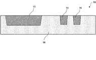
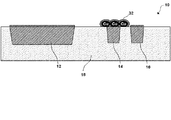
【解決手段】半導体装置10は、ダマシン配線からなる配線層を有し、0.5μm以上の幅を有する第1の配線12と、前記第1の配線12に隣接し前記第1の配線12から0.5μm未満の間隔で配置された第2の配線14と、前記第2の配線14に隣接し前記第1の配線12から0.5μm以下の間隔で配置された第3の配線16と、を備え、前記第2および第3の配線は同電位を有するよう構成されている。
【選択図】図1
Description
距離0.3μm: 3atmic%
距離0.5μm: 検出限界以下
距離0.7μm: 検出限界以下
距離1.4μm: 検出限界以下
であった。したがって、太幅配線である配線12と細幅配線である配線14との間隔が0.5μm未満で配置され、かつ太幅配線である配線12と細幅配線である配線16との間隔が0.5μm以下で配置された場合に、配線14と配線16が同電位を有するように構成する必要がある。
12 配線(第1の配線)
14 配線(第2の配線)
16 配線(第3の配線)
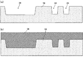
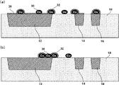
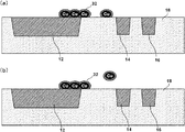
18 層間絶縁膜
20 配線溝
22 配線溝
24 配線溝
26 Cu膜
28 酸化防止膜
30 Cu
32 Cuと有機物を含む錯体
34 酸化防止膜
Claims (8)
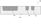
- ダマシン配線からなる配線層を有する半導体装置において、
0.5μm以上の幅を有する第1の配線と、
前記第1の配線に隣接し前記第1の配線から0.5μm未満の間隔で配置された第2の配線と、
前記第2の配線に隣接し前記第1の配線から0.5μm以下の間隔で配置された第3の配線と、を備え、
前記第2および第3の配線は同電位を有するよう構成されていることを特徴とする半導体装置。 - 請求項1に記載の半導体装置において、
前記第1の配線と前記第2の配線の間隔が0.2μm以上である半導体装置。 - 請求項1または2に記載の半導体装置において、
前記第1、第2、および第3の配線は平行に配置されている半導体装置。 - 請求項1乃至3いずれかに記載の半導体装置において、
前記第2の配線と前記第3の配線の配線ピッチが、0.15μm未満である半導体装置。 - 請求項1乃至4いずれかに記載の半導体装置において、
前記第2および第3の配線は、最小ピッチ配線である半導体装置。 - 請求項1乃至5いずれかに記載の半導体装置において、
前記第2および第3の配線は接地電位を有する半導体装置。 - 請求項1乃至5いずれかに記載の半導体装置において、
前記第2および第3の配線は電源電位を有する半導体装置。 - 請求項1乃至7いずれかに記載の半導体装置において、
前記第1、第2、および第3の配線は、銅含有金属である半導体装置。
Priority Applications (3)
| Application Number | Priority Date | Filing Date | Title |
|---|---|---|---|
| JP2008145372A JP5350681B2 (ja) | 2008-06-03 | 2008-06-03 | 半導体装置 |
| US12/474,526 US8299621B2 (en) | 2008-06-03 | 2009-05-29 | Semiconductor device having wiring layer with a wide wiring and fine wirings |
| US13/561,752 US8426975B2 (en) | 2008-06-03 | 2012-07-30 | Semiconductor device having wiring layer with a wide wiring and fine wirings |
Applications Claiming Priority (1)
| Application Number | Priority Date | Filing Date | Title |
|---|---|---|---|
| JP2008145372A JP5350681B2 (ja) | 2008-06-03 | 2008-06-03 | 半導体装置 |
Publications (2)
| Publication Number | Publication Date |
|---|---|
| JP2009295653A true JP2009295653A (ja) | 2009-12-17 |
| JP5350681B2 JP5350681B2 (ja) | 2013-11-27 |
Family
ID=41378787
Family Applications (1)
| Application Number | Title | Priority Date | Filing Date |
|---|---|---|---|
| JP2008145372A Active JP5350681B2 (ja) | 2008-06-03 | 2008-06-03 | 半導体装置 |
Country Status (2)
| Country | Link |
|---|---|
| US (2) | US8299621B2 (ja) |
| JP (1) | JP5350681B2 (ja) |
Families Citing this family (1)
| Publication number | Priority date | Publication date | Assignee | Title |
|---|---|---|---|---|
| US9553043B2 (en) * | 2012-04-03 | 2017-01-24 | Taiwan Semiconductor Manufacturing Company, Ltd. | Interconnect structure having smaller transition layer via |
Citations (5)
| Publication number | Priority date | Publication date | Assignee | Title |
|---|---|---|---|---|
| JPH10294366A (ja) * | 1997-04-21 | 1998-11-04 | Matsushita Electric Ind Co Ltd | 半導体装置及びその製造方法 |
| JP2003133314A (ja) * | 2001-10-30 | 2003-05-09 | Hitachi Ltd | 半導体装置の製造方法 |
| JP2005005562A (ja) * | 2003-06-13 | 2005-01-06 | Nec Electronics Corp | 半導体集積回路の自動配線方法、そのプログラム及び半導体集積回路 |
| JP2005268748A (ja) * | 2004-02-18 | 2005-09-29 | Nec Electronics Corp | 半導体装置及びその製造方法 |
| JP2005535118A (ja) * | 2002-07-29 | 2005-11-17 | シンプリシティ・インコーポレーテッド | 集積回路デバイスと集積回路デバイスを設計するための方法及び装置 |
Family Cites Families (20)
| Publication number | Priority date | Publication date | Assignee | Title |
|---|---|---|---|---|
| US6265780B1 (en) * | 1998-12-01 | 2001-07-24 | United Microelectronics Corp. | Dual damascene structure for the wiring-line structures of multi-level interconnects in integrated circuit |
| JP2000216264A (ja) * | 1999-01-22 | 2000-08-04 | Mitsubishi Electric Corp | Cmos論理回路素子、半導体装置とその製造方法およびその製造方法において用いる半導体回路設計方法 |
| JP4030257B2 (ja) * | 2000-08-14 | 2008-01-09 | 株式会社ルネサステクノロジ | 半導体集積回路装置 |
| JP3566203B2 (ja) * | 2000-12-06 | 2004-09-15 | 株式会社東芝 | 半導体装置及びその製造方法 |
| JP2002217195A (ja) * | 2001-01-17 | 2002-08-02 | Mitsubishi Electric Corp | 半導体装置およびその製造方法 |
| TW584899B (en) * | 2001-07-20 | 2004-04-21 | Nutool Inc | Planar metal electroprocessing |
| US6989603B2 (en) * | 2001-10-02 | 2006-01-24 | Guobiao Zhang | nF-Opening Aiv Structures |
| JP3790469B2 (ja) * | 2001-12-21 | 2006-06-28 | 富士通株式会社 | 半導体装置 |
| US7042095B2 (en) * | 2002-03-29 | 2006-05-09 | Renesas Technology Corp. | Semiconductor device including an interconnect having copper as a main component |
| JP4034227B2 (ja) | 2002-05-08 | 2008-01-16 | Necエレクトロニクス株式会社 | 半導体装置の製造方法 |
| CN101673754B (zh) * | 2004-05-25 | 2011-11-30 | 瑞萨电子株式会社 | 半导体器件 |
| US7791163B2 (en) * | 2004-10-25 | 2010-09-07 | Renesas Technology Corp. | Semiconductor device and its manufacturing method |
| JP4803997B2 (ja) | 2004-12-03 | 2011-10-26 | ルネサスエレクトロニクス株式会社 | 半導体集積装置、その設計方法、設計装置、およびプログラム |
| JP2007035955A (ja) * | 2005-07-27 | 2007-02-08 | Toshiba Corp | 半導体装置およびその製造方法 |
| US7446040B2 (en) * | 2006-01-12 | 2008-11-04 | International Business Machines Corporation | Structure for optimizing fill in semiconductor features deposited by electroplating |
| US20080122089A1 (en) * | 2006-11-08 | 2008-05-29 | Toshiba America Electronic Components, Inc. | Interconnect structure with line resistance dispersion |
| JP4688901B2 (ja) * | 2008-05-13 | 2011-05-25 | 三菱電機株式会社 | 半導体装置 |
| JP5522622B2 (ja) * | 2009-03-18 | 2014-06-18 | ピーエスフォー ルクスコ エスエイアールエル | 半導体記憶装置及びその製造方法 |
| CN102576709B (zh) * | 2010-08-17 | 2015-03-04 | 松下电器产业株式会社 | 非易失性存储装置及其制造方法 |
| JP5569354B2 (ja) * | 2010-11-17 | 2014-08-13 | 富士通セミコンダクター株式会社 | キャパシタおよび半導体装置 |
-
2008
- 2008-06-03 JP JP2008145372A patent/JP5350681B2/ja active Active
-
2009
- 2009-05-29 US US12/474,526 patent/US8299621B2/en not_active Expired - Fee Related
-
2012
- 2012-07-30 US US13/561,752 patent/US8426975B2/en active Active
Patent Citations (5)
| Publication number | Priority date | Publication date | Assignee | Title |
|---|---|---|---|---|
| JPH10294366A (ja) * | 1997-04-21 | 1998-11-04 | Matsushita Electric Ind Co Ltd | 半導体装置及びその製造方法 |
| JP2003133314A (ja) * | 2001-10-30 | 2003-05-09 | Hitachi Ltd | 半導体装置の製造方法 |
| JP2005535118A (ja) * | 2002-07-29 | 2005-11-17 | シンプリシティ・インコーポレーテッド | 集積回路デバイスと集積回路デバイスを設計するための方法及び装置 |
| JP2005005562A (ja) * | 2003-06-13 | 2005-01-06 | Nec Electronics Corp | 半導体集積回路の自動配線方法、そのプログラム及び半導体集積回路 |
| JP2005268748A (ja) * | 2004-02-18 | 2005-09-29 | Nec Electronics Corp | 半導体装置及びその製造方法 |
Also Published As
| Publication number | Publication date |
|---|---|
| US8299621B2 (en) | 2012-10-30 |
| JP5350681B2 (ja) | 2013-11-27 |
| US20120292765A1 (en) | 2012-11-22 |
| US20090294980A1 (en) | 2009-12-03 |
| US8426975B2 (en) | 2013-04-23 |
Similar Documents
| Publication | Publication Date | Title |
|---|---|---|
| JP5067039B2 (ja) | 半導体装置の製造方法 | |
| JP4963349B2 (ja) | 半導体装置の製造方法 | |
| JP5012022B2 (ja) | 半導体装置及びその製造方法 | |
| TWI546962B (zh) | 半導體裝置及半導體裝置之製造方法 | |
| US10475700B2 (en) | Etching to reduce line wiggling | |
| JP4234019B2 (ja) | 相互接続層をリワークする方法 | |
| CN101079408A (zh) | 双镶嵌结构及其制造方法 | |
| JP5380838B2 (ja) | 半導体装置の製造方法 | |
| KR20160081423A (ko) | 결함 검출 방법 및 결함 검출 시스템 | |
| CN101335256B (zh) | Nor闪存装置及制造该装置的方法 | |
| JP2010225682A (ja) | 半導体装置およびその製造方法 | |
| JP2009170846A (ja) | 半導体装置およびその製造方法 | |
| JP5313474B2 (ja) | 半導体装置およびその製造方法 | |
| JP5350681B2 (ja) | 半導体装置 | |
| US20110298133A1 (en) | Semiconductor device | |
| TWI423344B (zh) | 半導體裝置及其製造方法 | |
| JP5388478B2 (ja) | 半導体装置 | |
| JP5942867B2 (ja) | 半導体装置の製造方法 | |
| JP2012164704A (ja) | 半導体装置の製造方法および半導体装置 | |
| JP2003257969A (ja) | 半導体装置 | |
| CN1476077A (zh) | 多层配线的形成方法及其检查方法 | |
| JP4349269B2 (ja) | 半導体装置及びその製造方法 | |
| JP5380929B2 (ja) | 半導体装置及びその製造方法 | |
| JP2010232239A (ja) | 半導体装置 | |
| KR20080047541A (ko) | 반도체 장치 상에 캐핑 레이어를 형성하는 방법 |
Legal Events
| Date | Code | Title | Description |
|---|---|---|---|
| RD01 | Notification of change of attorney |
Free format text: JAPANESE INTERMEDIATE CODE: A7421 Effective date: 20100426 |
|
| A621 | Written request for application examination |
Free format text: JAPANESE INTERMEDIATE CODE: A621 Effective date: 20110308 |
|
| A977 | Report on retrieval |
Free format text: JAPANESE INTERMEDIATE CODE: A971007 Effective date: 20130228 |
|
| A131 | Notification of reasons for refusal |
Free format text: JAPANESE INTERMEDIATE CODE: A131 Effective date: 20130305 |
|
| TRDD | Decision of grant or rejection written | ||
| A01 | Written decision to grant a patent or to grant a registration (utility model) |
Free format text: JAPANESE INTERMEDIATE CODE: A01 Effective date: 20130820 |
|
| A61 | First payment of annual fees (during grant procedure) |
Free format text: JAPANESE INTERMEDIATE CODE: A61 Effective date: 20130822 |
|
| R150 | Certificate of patent or registration of utility model |
Ref document number: 5350681 Country of ref document: JP Free format text: JAPANESE INTERMEDIATE CODE: R150 Free format text: JAPANESE INTERMEDIATE CODE: R150 |
|
| S531 | Written request for registration of change of domicile |
Free format text: JAPANESE INTERMEDIATE CODE: R313531 |
|
| R350 | Written notification of registration of transfer |
Free format text: JAPANESE INTERMEDIATE CODE: R350 |