JP2009302995A - Method of manufacturing piezoelectric device - Google Patents
Method of manufacturing piezoelectric device Download PDFInfo
- Publication number
- JP2009302995A JP2009302995A JP2008156294A JP2008156294A JP2009302995A JP 2009302995 A JP2009302995 A JP 2009302995A JP 2008156294 A JP2008156294 A JP 2008156294A JP 2008156294 A JP2008156294 A JP 2008156294A JP 2009302995 A JP2009302995 A JP 2009302995A
- Authority
- JP
- Japan
- Prior art keywords
- package body
- package
- bare chip
- opening
- piezoelectric
- Prior art date
- Legal status (The legal status is an assumption and is not a legal conclusion. Google has not performed a legal analysis and makes no representation as to the accuracy of the status listed.)
- Withdrawn
Links
Images

Classifications
-
- H—ELECTRICITY
- H10—SEMICONDUCTOR DEVICES; ELECTRIC SOLID-STATE DEVICES NOT OTHERWISE PROVIDED FOR
- H10W—GENERIC PACKAGES, INTERCONNECTIONS, CONNECTORS OR OTHER CONSTRUCTIONAL DETAILS OF DEVICES COVERED BY CLASS H10
- H10W72/00—Interconnections or connectors in packages
- H10W72/851—Dispositions of multiple connectors or interconnections
- H10W72/874—On different surfaces
- H10W72/884—Die-attach connectors and bond wires
-
- H—ELECTRICITY
- H10—SEMICONDUCTOR DEVICES; ELECTRIC SOLID-STATE DEVICES NOT OTHERWISE PROVIDED FOR
- H10W—GENERIC PACKAGES, INTERCONNECTIONS, CONNECTORS OR OTHER CONSTRUCTIONAL DETAILS OF DEVICES COVERED BY CLASS H10
- H10W90/00—Package configurations
- H10W90/701—Package configurations characterised by the relative positions of pads or connectors relative to package parts
- H10W90/751—Package configurations characterised by the relative positions of pads or connectors relative to package parts of bond wires
- H10W90/754—Package configurations characterised by the relative positions of pads or connectors relative to package parts of bond wires between a chip and a stacked insulating package substrate, interposer or RDL
Landscapes
- Oscillators With Electromechanical Resonators (AREA)
- Piezo-Electric Or Mechanical Vibrators, Or Delay Or Filter Circuits (AREA)
Abstract
Description
本発明は、圧電デバイスの製造方法に関し、特に加熱工程を減らし、使用する接着剤、
ICへの熱ストレスを低減した圧電デバイスの製造方法に関するものである。
The present invention relates to a method for manufacturing a piezoelectric device, particularly an adhesive that reduces and uses a heating step,
The present invention relates to a method of manufacturing a piezoelectric device that reduces thermal stress on an IC.
圧電デバイス、特に水晶デバイスは周波数安定度、小型軽量、低価格等により携帯電話
等の通信機器から水晶時計のような民生機器まで、多くの分野で用いられている。水晶振
動子の周波数温度特性を補償した温度補償型圧電発振器(TCXO)は、周波数安定度を
必要とする携帯電話等に広く用いられている。
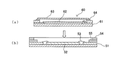
特許文献1には、能動素子を実装したパッケージと、振動素子を実装したパッケージと
を積層して構成した発振器が開示されている。この発振器は、上面が開口し内部に能動素
子52が実装された第1パッケージ本体51と、振動素子62が実装され第1パッケージ
本体51よりも小さく上面が開口した第2パッケージ本体61と、第2パッケージ本体6
1の上面開口部に装着された封止板63と、を備え、第1パッケージ本体51の上面に第
2パッケージ本体61を接合し、第2パッケージ本体61の接続電極と、第1パッケージ
本体51の接続電極とを電気的に接続して構成される。
Piezoelectric devices, particularly quartz devices, are used in many fields from communication devices such as mobile phones to consumer devices such as quartz watches due to their frequency stability, small size and light weight, and low price. A temperature-compensated piezoelectric oscillator (TCXO) that compensates the frequency-temperature characteristics of a crystal resonator is widely used in mobile phones and the like that require frequency stability.
A
第1パッケージ本体51はセラミックシートの積層体で形成され、その形状は図5(b
)の断面図に示すように上面が開口した箱型に成形されている。この第1パッケージ本体
51の内部には、ベアチップよりなる能動素子(IC)52が接着剤により固定されて実
装されている。能動素子52は、図に示すようにボンディングワイヤ53により第1パッ
ケージ本体51内に設けた電極端子と電気的に接続され、第1パッケージ本体51の外周
壁の接続電極と接続されている。
振動ユニット60は、図5(a)の断面図に示すようにセラミックシートの積層体で形
成され、上面が開口した第2パッケージ本体61と、該第2パッケージ本体61の内部に
実装された水晶振動素子62と、第2パッケージ本体61の開口部を気密封止する金属蓋
63と、を備えている。第2パッケージ本体61の外周壁の上に固定したシームリング6
4に金属蓋63を溶接することによって振動素子62を第2パッケージ本体61の内部に
気密封止している。
図5(b)に示すように、第1パッケージ本体51の外周壁54の上面内周部に凹状の
段差部55を形成し、この段差部55の上に第2パッケージ本体61を支持させれば、第
1パッケージ本体51における第2パッケージ本体61の位置決めがなされ、第1、第2
の夫々の接続電極の相対位置も正しく設定され、両者の電気的接続が確実に行われると共
に、第1パッケージ本体51の上面開口部は第2パッケージ本体61で確実に封止される
。
As shown in the cross-sectional view of FIG. Inside the
As shown in the cross-sectional view of FIG. 5A, the
4, the
As shown in FIG. 5B, a concave
The relative positions of the respective connection electrodes are also set correctly so that the electrical connection between them is reliably performed, and the upper surface opening of the
しかしながら、特許文献1に開示された積層型の発振器では、第2パッケージ本体61
内に水晶振動素子62を実装し、第2パッケージ本体61のシームリング64に金属蓋6
3を溶接して振動ユニット60を構成する工程と、第1パッケージ本体51の底面に導電
性接着剤を用いて能動素子52を接着し、ボンディングワイヤで接続する実装工程と、第
1パッケージ本体51の上面に第2パッケージ本体61を接合して樹脂で封止すると共に
第1及び第2の接続電極を接続する工程と、が必要であり、工程が複雑であると共に加熱
工程の回数が多く、IC(能動素子)、接着剤への熱ストレスの回数が多いという問題が
あった。また、第1パッケージ本体51が樹脂封止では気密性が保たれない虞があり、I
C(能動素子)を樹脂(ポッティング剤)で保護しなければならず、該樹脂によりIC(
能動素子)の接着に用いる導電性接着剤、つまりAgペースト樹脂の剥離が生じるという
問題があった。
本発明は上記問題を解決するためになされたもので、加熱工程が少なく、IC保護用の
ポッティング剤を必要しない圧電デバイスの製造方法を提供することにある。
However, in the stacked oscillator disclosed in
A
3, forming a
C (active element) must be protected with a resin (potting agent), and the resin (IC (
There is a problem that peeling of the conductive adhesive used for bonding the active element), that is, the Ag paste resin occurs.
The present invention has been made to solve the above-described problems, and it is an object of the present invention to provide a method for manufacturing a piezoelectric device that requires few heating steps and does not require a potting agent for IC protection.
本発明は、上記の課題の少なくとも一部を解決するためになされたものであり、以下の
形態又は適用例として実現することが可能である。
SUMMARY An advantage of some aspects of the invention is to solve at least a part of the problems described above, and the invention can be implemented as the following forms or application examples.
[適用例1]本発明に係る圧電デバイスの製造方法は、第1の絶縁基板の凹所内に圧電
振動素子を収容した第1パッケージ本体、又は第2の絶縁基板の凹所内にベアチップを収
容した第2パッケージ本体の何れか一方のパッケージ本体の開口部に他方のパッケージ本
体の底面を重ね合わせると共に、他方のパッケージ本体の開口部に蓋体を重ね合わせる工
程と、前記一方のパッケージ本体の開口部と他方のパッケージ本体の底面との間のガラス
部材と、前記他方のパッケージ本体の開口部と前記蓋体との間のガラス部材、及び前記一
方のパッケージ本体の開口部と他方のパッケージ本体の底面との間のポリイミド系の導電
性接着剤を加熱する工程と、備えることを特徴とする。
Application Example 1 In the piezoelectric device manufacturing method according to the present invention, the first package body in which the piezoelectric vibration element is accommodated in the recess of the first insulating substrate, or the bare chip is accommodated in the recess of the second insulating substrate. A step of superimposing a bottom surface of the other package main body on an opening of one of the second package main bodies and an overlap of a lid on the opening of the other package main body, and an opening of the one package main body And a glass member between the other package body, a glass member between the opening of the other package body and the lid, and an opening of the one package body and the bottom of the other package body And a step of heating a polyimide-based conductive adhesive therebetween.
以上のような圧電デバイスの製造方法を用いて圧電デバイスを製造すると、第1及び第
2パッケージ本体ともガラス封止により気密性は完全であり、ベアチップICに樹脂でコ
ーティング(ポッティング剤)する必要もなく、第2パッケージ本体の内部底面にベアチ
ップICの接着のために用いた導電性接着剤が、ポッティング剤により剥離(デラミネー
ション)するという虞も無くなる利点がある。
また、加熱工程は、圧電振動素子を第1パッケージ本体に導通固定する接着剤の加熱工
程と、ベアチップICを第2パッケージ本体に導通固定する接着剤の加熱工程と、第1及
び第2パッケージ本体をガラス封止するための加熱工程と、の3回であり、加熱工程によ
る圧電振動素子、導電性接着剤、ベアチップIC等への悪影響も減少させることができる
という効果がある。
When a piezoelectric device is manufactured using the above-described method for manufacturing a piezoelectric device, both the first and second package bodies are completely sealed by glass sealing, and the bare chip IC needs to be coated with a resin (potting agent). In addition, there is an advantage that there is no possibility that the conductive adhesive used for bonding the bare chip IC to the inner bottom surface of the second package body is peeled (delaminated) by the potting agent.
In addition, the heating process includes an adhesive heating process for electrically fixing the piezoelectric vibration element to the first package body, an adhesive heating process for electrically fixing the bare chip IC to the second package body, and the first and second package bodies. The heating process for sealing the glass with glass is three times, and there is an effect that adverse effects on the piezoelectric vibration element, conductive adhesive, bare chip IC and the like by the heating process can be reduced.
[適用例2]また、圧電デバイスの製造方法は、前記蓋体の裏面、及び前記一方のパッ
ケージ本体の上面に、前記ガラス部材が予め塗布されていることを特徴とする適用例1に
記載の圧電デバイスの製造方法である。
Application Example 2 In addition, in the method for manufacturing a piezoelectric device, the glass member is preliminarily applied to the back surface of the lid body and the upper surface of the one package body. It is a manufacturing method of a piezoelectric device.
以上のように、蓋体の一方の面と、一方のパッケージ本体の開口部の上面に予めガラス
部材を塗布しておくことにより、作業効率が改善されるという効果がある。
As described above, there is an effect that the working efficiency is improved by applying the glass member in advance to one surface of the lid and the upper surface of the opening of one package body.
[適用例3]また、圧電デバイスの製造方法は、前記一方のパッケージ本体の上面の一
部には、前記導電性接着剤が予め塗布されていることを特徴とする請求項1又は2に記載
の圧電デバイスの製造方法である。
Application Example 3 In the method for manufacturing a piezoelectric device, the conductive adhesive is preliminarily applied to a part of the upper surface of the one package body. This is a method for manufacturing the piezoelectric device.
以上のように、一方のパッケージ本体の端子電極に予め導電性のポリイミド樹脂を塗布
しておくことにより、作業効率が良くなると共に350℃という高温の工程を経ても、ポ
リイミド樹脂の特性により一方のパッケージ本体の端子電極と他方のパッケージ本体の端
子電極との導通が確実に行えるという利点がある。
As described above, by applying a conductive polyimide resin to the terminal electrode of one package body in advance, the working efficiency is improved and one of the characteristics of the polyimide resin is improved even after a high temperature process of 350 ° C. There is an advantage that conduction between the terminal electrode of the package body and the terminal electrode of the other package body can be reliably performed.
以下、本発明の実施の形態を図面に基づいて詳細に説明する。なお、本実施の形態では
、圧電デバイスとして水晶発振器を例に挙げて説明する。
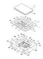
図1は、本発明に係る圧電デバイスの製造方法を用いて製造する圧電発振器の概略斜視
図である。圧電発振器は、圧電振動素子(水晶振動素子)3を実装した第1パッケージ本
体1と、ベアチップIC12を実装した第2パッケージ本体11と、第1パッケージ本体
1の開口部を気密封止する蓋体9と、を備えている。
第1パッケージ本体1は、例えば複数のセラミックシートの積層体で形成され、その形
状は図1の斜視図に示すように上面が開口した箱型となっている。図1に示した例では、
第1パッケージ本体1はセラミックシート1a、1b(図示せず)、1c、1dより構成
されている。第1パッケージ本体1の開口部2に形成された段差部8に導電性接着剤、例
えばポリイミド系の接着剤を塗布し、この導電性接着剤の上に水晶振動素子3を載置し、
加熱硬化させて、固定及び導通を図る。水晶振動素子3は、例えば所定の厚さに仕上げた
ATカット水晶基板4の両面に、励振電極5a、5b(図示せず)と、励振電極5a、5
bから水晶基板4の端部に延在する引き出し電極6a、6bと、を真空蒸着法等を用いて
形成する。水晶振動素子3の引き出し電極6a、6bは、段差部8に形成した端子電極を
介してセラミックシート1cの裏面に設けた端子電極7b、7cと導通している。
Hereinafter, embodiments of the present invention will be described in detail with reference to the drawings. In this embodiment, a crystal oscillator will be described as an example of a piezoelectric device.
FIG. 1 is a schematic perspective view of a piezoelectric oscillator manufactured using the method for manufacturing a piezoelectric device according to the present invention. The piezoelectric oscillator includes a
The
The
Fix and conduct by heat curing. The quartz resonator element 3 includes, for example, excitation electrodes 5a and 5b (not shown) and excitation electrodes 5a and 5 on both surfaces of an AT-cut quartz substrate 4 finished to a predetermined thickness.
The
第2パッケージ本体11は、第1パッケージ本体1と同様に複数のセラミックシートを
積層して形成され、その形状は図1の斜視図に示すように上面が開口した箱型となってい
る。第2パッケージ本体11の開口部13の底面には階段状に段差14、15a、15b
、16が形成されており、一番下の段差部14の上面に導電性接着剤、例えばポリイミド
系の接着剤を塗布し、該導電性接着剤の上にベアチップIC12を載置し、加熱乾燥させ
て固定する。ベアチップIC12の端子電極と、段差部15a、15b上に設けられた端
子電極と、をボンディングワイヤ17で接続する。段差部15a、15b上の端子電極は
、第2パッケージ本体11の外周壁の接続電極(キャスタレーション)18a、18b、
18c、18d及び19a、19b、19c、19dと導通している。また、第2パッケ
ージ本体11の外周壁の上面には端子電極20a、20b、20c、20dが形成されて
おり、これらは段差15a、15b上の端子電極と導通している。
さらに、段差部16上にはベアチップIC12の周囲を囲むように、ガラス封止材21
が塗布されている。
なお、ベアチップIC12には、水晶振動素子3を駆動する発振回路、水晶振動素子3
の周波数補償に用いられる可変容量素子、該可変容量素子に電圧を供給する補償電圧発生
回路、データと記憶するメモリ回路等が構成されている。
The
, 16 is formed, a conductive adhesive, for example, a polyimide-based adhesive is applied to the upper surface of the lowermost stepped portion 14, and the
18c, 18d and 19a, 19b, 19c, 19d are electrically connected. Further,
Further, the
Is applied.
The
A variable capacitance element used for frequency compensation, a compensation voltage generation circuit for supplying a voltage to the variable capacitance element, a memory circuit for storing data, and the like are configured.
図1に示すように蓋体9の裏面には、該蓋体9の周縁に沿ってガラス封止材22が塗布
されている。蓋体9の材質はセラミック材、ガラス材、金属材のいずれであってもよい。
第2パッケージ本体11の開口部13に第1パッケージ本体1の底部1aを嵌め込み、第
1パッケージ本体1の開口部2の周縁1cに蓋体9を載置する。嵌合した第1及び第2パ
ッケージ本体1、11と、第1パッケージ本体の上部に載置した蓋体9とを所定の温度の
加熱炉で所定の時間保持すことにより、ガラス封止材21、22は溶融し、水晶振動素子
3は第1パッケージ本体1と蓋体9により気密封止される。また、ベアチップIC12は
第1パッケージ本体1の底部1aと、第2パッケージ本体11の段差部16とにより、気
密封止される。加熱炉を例えば窒素N2ガスで満たすことにより、第1及び第2パッケー
ジ本体1、11内に窒素N2ガスを封入することが可能である。
As shown in FIG. 1, a
The bottom portion 1 a of the
図2は、水晶振動素子3を実装した第1パッケージ本体1、IC12を実装した第2パ
ッケージ本体11及び蓋体9が、ガラス封止材21、22にて気密封止され、一体化した
圧電発振器の斜視図である。
以上説明したように、本発明の製造方法を用いて水晶発振器を製造すると、第1及び第
2パッケージ本体1、11ともガラス封止により気密性は完全であり、ベアチップIC1
2に樹脂でコーティング(ポッティング剤)する必要もなく、第2パッケージ本体の内部
底面にベアチップICの接着のために用いた導電性接着剤が、ポッティング剤により剥離
(デラミネーション)するという虞も無くなる利点がある。
また、加熱工程は、圧電振動素子3を第1パッケージ本体1に導通固定する接着剤の加
熱工程と、ベアチップIC12を第2パッケージ本体に導通固定する接着剤の加熱工程と
、第1及び第2パッケージ本体1、11をガラス封止するための加熱工程と、の3回であ
り、加熱工程による圧電振動素子3、導電性接着剤、ベアチップIC12等への悪影響も
減少させることができるという効果がある。
また、蓋体9の一方の面と、一方のパッケージ本体の開口部の上面にガラス部材を予め
塗布しておくことにより、作業効率が改善されるという効果がある。
また、一方のパッケージ本体の端子電極に予め導電性のポリイミド樹脂を塗布しておく
ことにより、作業効率が良くなると共に350℃という高温下でもポリイミド樹脂特性に
より一方のパッケージ本体端子電極と他方のパッケージ本体の端子電極との導通が確実に
行えるという利点がある。
FIG. 2 shows an integrated piezoelectric device in which a
As described above, when the crystal oscillator is manufactured by using the manufacturing method of the present invention, the first and
There is no need to coat (potting agent) 2 with resin, and there is no possibility that the conductive adhesive used for bonding the bare chip IC to the inner bottom surface of the second package body will be peeled off (delamination) by the potting agent. There are advantages.
The heating process includes an adhesive heating process for electrically fixing the piezoelectric vibration element 3 to the
Moreover, there exists an effect that work efficiency is improved by apply | coating a glass member beforehand to the one surface of the cover body 9 and the upper surface of the opening part of one package main body.
Also, by applying a conductive polyimide resin to the terminal electrode of one package body in advance, the working efficiency is improved and the characteristics of one package body terminal electrode and the other package are improved due to the polyimide resin characteristics even at a high temperature of 350 ° C. There is an advantage that conduction with the terminal electrode of the main body can be reliably performed.
図3は、本発明に係る圧電デバイスの製造方法を用いて製造する他の圧電発振器の概略
断面図である。第1パッケージ本体1は複数のセラミックシート1a、1b、1c、1d
より構成されており、セラミックシート1aは導体薄膜25を内蔵し、該導体薄膜25は
セラミックシート1cの裏面に形成した電極7aと導通している。水晶振動素子3は第1
パッケージ本体1の段差部上に形成された端子電極10に導電性接着剤S1、例えばポリ
イミド系の接着剤で接着、固定され、該端子電極10はセラミックシート1cの裏面に形
成した電極7b、7c(図示せず)と導通している。セラミックシート1dの上部周縁に
はガラス封止材が塗布されている。
第2パッケージ本体11は、複数のセラミックシート11a、11b、11c、11d
より構成されており、セラミックシート11aは導体薄膜26を内蔵し、該導体薄膜26
は第2パッケージ本体11の外周壁の接続電極(キャスタレーション)18a〜18d及
び19a〜19dの何れかと導通し、接地される。第2パッケージ本体11の内底部(セ
ラミックシート11aの上面)に導電性接着剤S2、例えばポリイミド系の接着剤を塗布
し、該導電性接着剤S2上にベアチップIC12を載置する。ベアチップIC12の端子
電極と、セラミックシート11bの上面に形成した端子電極(図示せず)と、をボンディ
ングワイヤ17で接続すし、導電性接着剤S2を加熱炉内で硬化させて固定する。セラミ
ックシート11cの上面にはベアチップIC12を囲むようにガラス封止材22が塗布さ
れている。第2パッケージ本体11の上部(セラミックシート11dの上部)には端子電
極20a、20b、20c(図示せず)、20d(図示せず)が形成されおり、これらの
電極は外周壁の接続電極(キャスタレーション)18a〜18d及び19a〜19dの何
れかと導通している。
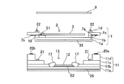
FIG. 3 is a schematic cross-sectional view of another piezoelectric oscillator manufactured using the method for manufacturing a piezoelectric device according to the present invention. The
The ceramic sheet 1a includes a conductive
The
The
The
Is electrically connected to one of the connection electrodes (castellation) 18a to 18d and 19a to 19d on the outer peripheral wall of the
第2パッケージ本体11の端子電極20a、20b、20c(図示せず)、20d(図
示せず)に導電性接着剤(ポリイミド系樹脂)を塗布し、開口部13に第1パッケージ本
体1の底部1a、1bを嵌め込む。嵌合した第1及び第2パッケージ本体1、11と、第
1パッケージ本体の上部に載置した蓋体9とを所定の温度の加熱炉で所定の時間保持すこ
とにより、ガラス封止材21、22は溶融し、水晶振動素子3は第1パッケージ本体1と
蓋体9により気密封止される。
図1及び3ではベアチップIC12の端子電極と、第2パッケージ本体11の端子電極
とをボンディングワイヤにより接続する例を示したが、ベアチップICをフリップチップ
ボンディングで接続してもよい。
A conductive adhesive (polyimide resin) is applied to the
1 and 3 show an example in which the terminal electrode of the
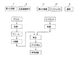
図4は、本発明に係る圧電発振器の製造フローを示す図である。なお、理解を容易にす
る為に、図1及び図3に付した符号を用いて説明する。始めに絶縁基板からなる第1及び
第2パッケージ本体1、11と、励振電極5a、5b及び引き出し電極6a、6bを形成
した水晶振動素子3と、ベアチップIC12と、裏面にガラス封止材を塗布した蓋体9と
、を用意する。
第1パッケージ本体1の凹所内(開口部2)の段差部8上に導電性接着剤を塗布し、そ
の上に水晶振動素子(圧電振動素子)3を載置(マウント)する。水晶振動素子3を載置
した第1パッケージ本体1を所定の温度の加熱炉内で所定の時間保持し、前記導電性接着
剤を乾燥し、その後、所定の温度のアニール装置内で所定の時間、アニール処理を行う。
アニール処理は水晶基板4(圧電基板)、電極薄膜5a、5b、接着剤等に残留する歪を
緩和するためである。さらに、所定の周波数に仕上げるため、励振電極5a、5b上に微
調整用の金属膜等を蒸着し、共振周波数を調整する。あるいは、励振電極から僅かに薄膜
を除去して周波数を調整してもよい。
FIG. 4 is a diagram showing a manufacturing flow of the piezoelectric oscillator according to the present invention. In order to facilitate understanding, description will be made using the reference numerals attached to FIGS. First, the first and
A conductive adhesive is applied on the stepped portion 8 in the recess (opening 2) of the
The annealing treatment is for relaxing strain remaining on the quartz substrate 4 (piezoelectric substrate), the electrode thin films 5a and 5b, the adhesive, and the like. Further, in order to finish to a predetermined frequency, a metal film for fine adjustment is deposited on the excitation electrodes 5a and 5b to adjust the resonance frequency. Alternatively, the frequency may be adjusted by slightly removing the thin film from the excitation electrode.
並行して、第2パッケージ本体11の凹所内(開口部13)の底部に導電性接着剤を塗
布し、該導電性接着剤上にベアチップIC12を載置する。ベアチップIC12の端子電
極と、第2パッケージ本体11の内底部に設けた端子電極と、をボンディングワイヤにて
接続する(ICマウント)。
ベアチップIC12を搭載した第2パッケージ本体11を、所定の温度の加熱炉内で所
定の時間保持し、前記導電性接着剤を乾燥する。乾燥処理が終了した第2パッケージ本体
11を取り出し、その後、第2パッケージ本体11の凹所内(開口部13)の底部であっ
て、ベアチップIC12の周縁にガラス封止材21を塗布する。あるいは、予めガラス封
止材21を塗布した第2パッケージ本体11を用意してもよい。その後、第2パッケージ
本体11の外周壁の上に形成した電極20a、20b、20c、20d上に導電性のポリ
イミド系樹脂を塗布する。
In parallel, a conductive adhesive is applied to the bottom of the recess (opening 13) of the
The
ベアチップIC12を収容(実装)した第2パッケージ本体11の凹所(開口部13)
に、水晶振動素子3を実装した第1パッケージ本体1の底部を嵌め込む。第1パッケージ
本体1の底部と、第2パッケージ本体に塗布したガラス封止材21と、が接し、第1パッ
ケージ本体1のつば(図3の1c)の裏面に形成した電極7a、7b、7c、7dと、第
2パッケージ本体11の外周壁の上に形成した電極20a、20b、20c、20dと、
が導電性のポリイミド系樹脂を介して接する。更に、ガラス封止材を塗布した蓋体9を第
1パッケージ本体1の開口部2に重ねる。嵌合した第1及び第2パッケージ本体1、11
を所定の温度、例えば350℃の加熱炉で所定の時間保持すると、蓋体9と、第2パッケ
ージ本体11の凹部底面と、に塗布したガラス封止材21、22が溶融して第1及び第2
パッケージ本体1、11が気密封止されると共に、前記導電性のポリイミド系樹脂が硬化
して第1パッケージ本体1の電極7a、7b、7c、7dと、第2パッケージ本体の20
a、20b、20c、20dとが夫々導通する。ポリイミド系の導電性接着剤は350℃
の高温に耐用するように作られている。
その後、圧電発振器の特性検査、例えば電気的特性を従来の手法で検査する。
Recessed portion (opening 13) of
The bottom portion of the
Are in contact via a conductive polyimide resin. Further, the lid body 9 coated with the glass sealing material is overlaid on the
Is held in a heating furnace at a predetermined temperature, for example, 350 ° C. for a predetermined time, the
The
a, 20b, 20c, and 20d are electrically connected. Polyimide conductive adhesive is 350 ° C
It is made to withstand high temperatures.
Thereafter, a characteristic inspection of the piezoelectric oscillator, for example, an electric characteristic is inspected by a conventional method.
図1、図3の例では圧電振動素子を収容する第1パッケージ本体1で、セラミックシー
ト1cが他のセラミックシートより大きくした例を示したが、第2パッケージ本体11の
ように外周壁は一様の幅寸法であってもよい。この場合は、第2の外周壁の上端と、第1
パッケージ本体の底部周縁とを接合するようにすればよい。また、第1の外周壁の上端と
、第2パッケージ本体の底部周縁とを接合するようにしてもよい。
ガラス封止材は、第1パッケージ本体1の上部周縁(セラミックシート1d上)と、第
2パッケージ本体の段差部16上と、に塗布してもよい。要は第1及び第2パッケージ本
体が共に気密封止できればよい。また、ガラス封止材は予め塗布しておいた方が作業の効
率がよくなる。
また、ガラス封止剤の代わりに樹脂封止剤を用いてもよい。
1 and 3 show an example in which the ceramic sheet 1c is larger than the other ceramic sheets in the first package
What is necessary is just to join the bottom part periphery of a package main body. Further, the upper end of the first outer peripheral wall and the bottom peripheral edge of the second package body may be joined.
The glass sealing material may be applied to the upper peripheral edge (on the
Further, a resin sealant may be used instead of the glass sealant.
1…第1パッケージ本体、2、13…開口部、3…圧電振動素子、4…圧電基板、5a
…励振電極、6a…引出電極、7a、7b、7c、7d…端子電極、8…段差部、9…蓋
体、11…第2パッケージ本体、12…ベアチップIC、14、15a、15b、16…
段差部、17…ボンディングワイヤ、18a、18b、18c、18d…外周壁電極(キ
ャスタレーション)、19a、19b、19c、19d…外周壁電極(キャスタレーショ
ン)、20a、20b、20c、20d…端子電極、21、22…ガラス封止材、S1、
S2…導電性接着剤、25、26…導体薄膜
DESCRIPTION OF
... excitation electrode, 6a ... extraction electrode, 7a, 7b, 7c, 7d ... terminal electrode, 8 ... stepped portion, 9 ... lid body, 11 ... second package body, 12 ... bare chip IC, 14, 15a, 15b, 16 ...
Stepped portion, 17 ... bonding wire, 18a, 18b, 18c, 18d ... outer peripheral wall electrode (castellation), 19a, 19b, 19c, 19d ... outer peripheral wall electrode (castellation), 20a, 20b, 20c, 20d ... terminal electrode , 21, 22 ... Glass sealing material, S1,
S2: Conductive adhesive, 25, 26 ... Conductor thin film
Claims (3)
縁基板の凹所内にベアチップを収容した第2パッケージ本体の何れか一方のパッケージ本
体の開口部に他方のパッケージ本体の底面を重ね合わせると共に、他方のパッケージ本体
の開口部に蓋体を重ね合わせる工程と、
前記一方のパッケージ本体の開口部と他方のパッケージ本体の底面との間のガラス部材
と、前記他方のパッケージ本体の開口部と前記蓋体との間のガラス部材、及び前記一方の
パッケージ本体の開口部と他方のパッケージ本体の底面との間のポリイミド系の導電性接
着剤を加熱する工程と、
を備えることを特徴とする圧電デバイスの製造方法。 One of the first package main body containing the piezoelectric vibration element in the recess of the first insulating substrate and the second package main body containing the bare chip in the recess of the second insulating substrate, and the other in the opening of the package main body. A process of superimposing the bottom surface of the package body and a cover body on the opening of the other package body;
A glass member between the opening of the one package body and the bottom surface of the other package body, a glass member between the opening of the other package body and the lid, and the opening of the one package body Heating a polyimide-based conductive adhesive between the portion and the bottom surface of the other package body,
A method for manufacturing a piezoelectric device comprising:
されていることを特徴とする請求項1に記載の圧電デバイスの製造方法。 The method for manufacturing a piezoelectric device according to claim 1, wherein the glass member is preliminarily applied to the back surface of the lid and the top surface of the one package body.
ことを特徴とする請求項1又は2に記載の圧電デバイスの製造方法。 3. The method of manufacturing a piezoelectric device according to claim 1, wherein the conductive adhesive is preliminarily applied to a part of an upper surface of the one package body. 4.
Priority Applications (1)
| Application Number | Priority Date | Filing Date | Title |
|---|---|---|---|
| JP2008156294A JP2009302995A (en) | 2008-06-16 | 2008-06-16 | Method of manufacturing piezoelectric device |
Applications Claiming Priority (1)
| Application Number | Priority Date | Filing Date | Title |
|---|---|---|---|
| JP2008156294A JP2009302995A (en) | 2008-06-16 | 2008-06-16 | Method of manufacturing piezoelectric device |
Publications (1)
| Publication Number | Publication Date |
|---|---|
| JP2009302995A true JP2009302995A (en) | 2009-12-24 |
Family
ID=41549411
Family Applications (1)
| Application Number | Title | Priority Date | Filing Date |
|---|---|---|---|
| JP2008156294A Withdrawn JP2009302995A (en) | 2008-06-16 | 2008-06-16 | Method of manufacturing piezoelectric device |
Country Status (1)
| Country | Link |
|---|---|
| JP (1) | JP2009302995A (en) |
Cited By (2)
| Publication number | Priority date | Publication date | Assignee | Title |
|---|---|---|---|---|
| JP2016195345A (en) * | 2015-04-01 | 2016-11-17 | 京セラクリスタルデバイス株式会社 | Piezoelectric device and manufacturing method thereof |
| CN115360149A (en) * | 2022-07-07 | 2022-11-18 | 昆山翔宁芯研精密电子有限公司 | Chip packaging structure and packaging process |
-
2008
- 2008-06-16 JP JP2008156294A patent/JP2009302995A/en not_active Withdrawn
Cited By (2)
| Publication number | Priority date | Publication date | Assignee | Title |
|---|---|---|---|---|
| JP2016195345A (en) * | 2015-04-01 | 2016-11-17 | 京セラクリスタルデバイス株式会社 | Piezoelectric device and manufacturing method thereof |
| CN115360149A (en) * | 2022-07-07 | 2022-11-18 | 昆山翔宁芯研精密电子有限公司 | Chip packaging structure and packaging process |
Similar Documents
| Publication | Publication Date | Title |
|---|---|---|
| KR101841767B1 (en) | Manufacturing method of electronic device package, electronic device package, and oscillator | |
| US8530986B2 (en) | Manufacturing method of electronic device package, electronic device package, and oscillator | |
| JP2002319838A (en) | Piezoelectric device and its package | |
| JP2000341065A (en) | Manufacture of piezoelectric vibrator | |
| CN104009726B (en) | Electronic device and its glass sealing method | |
| TWI804937B (en) | Thermostatic Bath Type Piezoelectric Oscillator | |
| JP2009044753A (en) | Piezoelectric oscillator | |
| TWI792541B (en) | Thermostatic Bath Type Piezoelectric Oscillator | |
| JP2009302995A (en) | Method of manufacturing piezoelectric device | |
| JP2010081127A (en) | Crystal oscillator and method of manufacturing same | |
| JPH05199056A (en) | Manufacture of piezoelectric vibrator | |
| JP4730419B2 (en) | Method for manufacturing piezoelectric oscillator | |
| JP4730418B2 (en) | Piezoelectric oscillator | |
| TWI827915B (en) | Constant temperature chamber piezoelectric oscillator | |
| JP2010166626A (en) | Piezoelectric device | |
| JP5432533B2 (en) | Manufacturing method of electronic device | |
| JP2009302996A (en) | Method of manufacturing piezoelectric device | |
| JP4384567B2 (en) | Manufacturing method of temperature compensated crystal oscillator | |
| JP5220539B2 (en) | Method for manufacturing piezoelectric vibrator | |
| JP5915179B2 (en) | Electronic device, oscillator, method for manufacturing electronic device, and method for manufacturing oscillator | |
| KR100891821B1 (en) | Manufacturing Method of Crystal Oscillator Package | |
| WO2021210214A1 (en) | Piezoelectric vibrator and method for manufacturing same | |
| CN121396080A (en) | Method for manufacturing oscillator | |
| JP2017085390A (en) | Crystal device | |
| JP4873980B2 (en) | Airtight package |
Legal Events
| Date | Code | Title | Description |
|---|---|---|---|
| A300 | Application deemed to be withdrawn because no request for examination was validly filed |
Free format text: JAPANESE INTERMEDIATE CODE: A300 Effective date: 20110906 |