JP2010077453A - Target for sputtering, transparent conductive film using the same and method of manufacturing the same - Google Patents
Target for sputtering, transparent conductive film using the same and method of manufacturing the same Download PDFInfo
- Publication number
- JP2010077453A JP2010077453A JP2008243468A JP2008243468A JP2010077453A JP 2010077453 A JP2010077453 A JP 2010077453A JP 2008243468 A JP2008243468 A JP 2008243468A JP 2008243468 A JP2008243468 A JP 2008243468A JP 2010077453 A JP2010077453 A JP 2010077453A
- Authority
- JP
- Japan
- Prior art keywords
- transparent conductive
- fluorine
- atomic
- target
- conductive film
- Prior art date
- Legal status (The legal status is an assumption and is not a legal conclusion. Google has not performed a legal analysis and makes no representation as to the accuracy of the status listed.)
- Withdrawn
Links
Images


Landscapes
- Non-Insulated Conductors (AREA)
- Manufacturing Of Electric Cables (AREA)
- Physical Vapour Deposition (AREA)
Abstract
【課題】 本発明は、低抵抗な膜を得るためのスパッタリング用ターゲットおよびそれを用いて形成される透明導電膜及びその製造方法を提供することを目的とする。
【解決手段】 酸化亜鉛、酸化アルミニウム及びフッ素を含有し、前記フッ素の量が全原子数に対して0.1原子%以上0.5原子%未満であるスパッタリング用ターゲット。また、酸化亜鉛、酸化アルミニウム及びフッ化アルミニウムを含有し、フッ素の量が全原子数に対して0.1原子以上0.5原子%未満であるターゲットを使用し、スパッタリングにより基板上に透明導電膜を形成する透明導電膜の製造方法。
【選択図】 図2PROBLEM TO BE SOLVED: To provide a sputtering target for obtaining a low resistance film, a transparent conductive film formed using the same, and a method for producing the same.
A sputtering target containing zinc oxide, aluminum oxide and fluorine, wherein the amount of the fluorine is 0.1 atomic% or more and less than 0.5 atomic% with respect to the total number of atoms. In addition, a transparent conductive material is formed on the substrate by sputtering using a target containing zinc oxide, aluminum oxide and aluminum fluoride, and the amount of fluorine being 0.1 atom or more and less than 0.5 atom% with respect to the total number of atoms. A method for producing a transparent conductive film for forming a film.
[Selection] Figure 2
Description
本発明は酸化亜鉛を主材料とするスパッタリング用ターゲットおよび該ターゲットを用いてなる透明導電膜及びその製造方法に関する。 The present invention relates to a sputtering target mainly composed of zinc oxide, a transparent conductive film using the target, and a method for producing the same.
従来主に使われている透明導電膜は、酸化インジウムに酸化錫を添加したITOや酸化錫に酸化アンチモン、フッ素をドープしたTAO、TFO等である。酸化インジウムに酸化錫を添加したITOはインジウムが希少金属で高価であるために、コスト高という問題があった。またTAOやTFOは透明性が低く、導電性も不十分であった。
一方で酸化亜鉛は資源が豊富にあり低コストで高い透明性や導電性、および化学的安定性を有しており、透明導電膜として注目されている。酸化亜鉛系透明導電膜はスパッタリング法をはじめとし、真空蒸着法、イオンプレーティング法、CVD法、めっき法など各種製膜法で形成させることが出来る。その中でもスパッタリング法は、比較的結晶性が良好で大面積に膜を形成させるのに適した方法である。
Conventionally used transparent conductive films are ITO in which tin oxide is added to indium oxide, TAO in which tin oxide is doped with antimony oxide, fluorine, TFO, and the like. ITO in which tin oxide is added to indium oxide has a problem of high cost because indium is a rare metal and expensive. TAO and TFO have low transparency and insufficient conductivity.
On the other hand, zinc oxide is abundant in resources, has low cost, high transparency, conductivity, and chemical stability, and has attracted attention as a transparent conductive film. The zinc oxide-based transparent conductive film can be formed by various film forming methods such as a vacuum evaporation method, an ion plating method, a CVD method, and a plating method, including a sputtering method. Among them, the sputtering method is a method that has relatively good crystallinity and is suitable for forming a film over a large area.
従来、酸化亜鉛膜にアルミニウムやガリウム等を添加することにより、高い導電性を得られることが知られている(例えば、特許文献1参照)。一方、酸化アルミニウムを添加した酸化亜鉛を用いてスパッタリング法により低抵抗な膜を形成することも提案されている。しかし従来の技術によれば、酸化亜鉛系透明導電膜が実用レベルにいたることはなかった。これは通常のスパッタリング法では放電空間で発生する高エネルギー荷電粒子が基板表面に入射することによって膜中に残留応力を発生させると共に、さまざまな結晶欠陥が生じる。その結果ドーピング効果の低下やキャリア移動度の減少により、膜の低抵抗化が妨げられていた。 Conventionally, it is known that high conductivity can be obtained by adding aluminum, gallium, or the like to a zinc oxide film (see, for example, Patent Document 1). On the other hand, it has also been proposed to form a low-resistance film by sputtering using zinc oxide to which aluminum oxide is added. However, according to the prior art, the zinc oxide-based transparent conductive film has not reached a practical level. In the normal sputtering method, high energy charged particles generated in the discharge space are incident on the substrate surface, thereby generating residual stress in the film and causing various crystal defects. As a result, lowering of the resistance of the film has been hindered by a decrease in doping effect and a decrease in carrier mobility.
本発明は、このような課題に対処しようとするものであり、低抵抗な膜を得るためのスパッタリング用ターゲットおよびそれを用いて形成される透明導電膜及びその製造方法を提供することを目的とする。 The present invention is intended to address such problems, and an object thereof is to provide a sputtering target for obtaining a low-resistance film, a transparent conductive film formed using the sputtering target, and a method for manufacturing the transparent conductive film. To do.
本発明は上述した課題を解決するために種々の研究を重ねた結果、酸化亜鉛を主材料とし、アルミニウムとフッ素が添加されたターゲットを用いることで本発明を完成するに至った。
前記課題を解決する第1の態様は、酸化亜鉛、酸化アルミニウム及びフッ素を含有し、前記フッ素の量が全原子数に対して0.1原子%以上0.5原子%未満であることを特徴とするスパッタリング用ターゲットである。
As a result of various studies to solve the above-described problems, the present invention has been completed by using a target containing zinc oxide as a main material and added with aluminum and fluorine.
A first aspect for solving the above problem is characterized in that it contains zinc oxide, aluminum oxide and fluorine, and the amount of the fluorine is 0.1 atomic% or more and less than 0.5 atomic% with respect to the total number of atoms. It is a sputtering target.
また、第2の態様は、第1の態様に加えて酸化アルミニウムの量が全原子数に対して1〜4原子%であることを特徴とするスパッタリング用ターゲットである。
また、第3の態様は、第1又は2の態様に加えてフッ化アルミニウムを含むことを特徴とするスパッタリング用ターゲットである。
また、本発明の透明導電膜は、前記第1乃至3の態様のスパッタリング用ターゲットを用いて得られることを特徴とする。
また、本発明の透明導電膜の製造方法は、酸化亜鉛、酸化アルミニウム及びフッ化アルミニウムを含有し、フッ素の量が全原子数に対して0.1原子%以上0.5原子%未満であるターゲットを使用し、スパッタリングにより基板上に透明導電膜を形成することを特徴とする。
The second aspect is a sputtering target characterized in that, in addition to the first aspect, the amount of aluminum oxide is 1 to 4 atomic% with respect to the total number of atoms.
The third aspect is a sputtering target characterized by containing aluminum fluoride in addition to the first or second aspect.
The transparent conductive film of the present invention is obtained using the sputtering target according to the first to third aspects.
The method for producing a transparent conductive film of the present invention contains zinc oxide, aluminum oxide, and aluminum fluoride, and the amount of fluorine is 0.1 atomic% or more and less than 0.5 atomic% with respect to the total number of atoms. A transparent conductive film is formed on a substrate by sputtering using a target.
本発明によればアルミニウム添加酸化亜鉛にさらにフッ素を添加したターゲットを用いて酸化亜鉛透明導電膜を作成することにより、従来の酸化亜鉛透明導電膜よりも低抵抗化を達成させることができた。
特許文献1では、フッ化亜鉛を用いて透明導電膜を作製しているが、フッ素の量が0.5〜3原子%である。本発明においては、0.5原子%未満と非常に微量でフッ素の低抵抗効果を発揮することができた。
According to the present invention, a resistance lower than that of a conventional zinc oxide transparent conductive film can be achieved by forming a zinc oxide transparent conductive film using a target obtained by further adding fluorine to aluminum-added zinc oxide.
In patent document 1, although the transparent conductive film is produced using zinc fluoride, the quantity of a fluorine is 0.5-3 atomic%. In the present invention, the low resistance effect of fluorine was able to be exhibited with a very small amount of less than 0.5 atomic%.
以下、本発明の実施の形態について図面を参照して説明する。
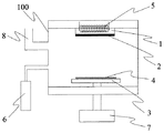
図1は本発明の透明導電膜の製造方法に適用するスパッタリング装置の一例を示す。スパッタリング装置においては真空排気系8とスパッタガス導入管6がチャンバ(スパッタ室)100と連結されている。
チャンバ100内にマグネットを内蔵した陰極3により支持されたターゲット4と透明導電膜を形成するガラス基板2を陽極1と対向配置する。
Hereinafter, embodiments of the present invention will be described with reference to the drawings.
FIG. 1 shows an example of a sputtering apparatus applied to the method for producing a transparent conductive film of the present invention. In the sputtering apparatus, a vacuum exhaust system 8 and a sputtering gas introduction pipe 6 are connected to a chamber (sputtering chamber) 100.
A
まず、チャンバ100内を2.0×10⁻³Torr以下まで減圧し、安定化させた後、セラミックヒータ5の電源を入れてガラス基板2を100℃程度に加熱し、アルゴンガスをスパッタガス導入管6からチャンバ100内に2.0×10⁻³Torr程度になるように供給する。
チャンバ100内の圧力は、1×10⁻³〜10×10−3Torrの範囲で調整するのが好ましい。1×10⁻³Torr未満の圧力では、放電が安定せず、異常放電しやすくなる。10×10−3Torrより高い圧力では、プラズマ密度が低くなり、スパッタ効率が悪くなると共に、粗密な膜になりやすい。
ガラス基板2の温度は100℃〜200℃の範囲で調整するのが好ましい。200℃より高い温度では抵抗率に起因する電子濃度の低下が起りやすく、100℃未満の温度では、抵抗率に起因する酸化亜鉛の結晶化が十分に行われなくなり、抵抗率の上昇が起りやすいためである。
First, the
The pressure in the
The temperature of the
次にチャンバ100内の圧力が安定した後、高周波電源7により陰極3に13.56MHzの高周波電力を印加し、100Wの出力でターゲット4をスパッタさせ、2時間堆積反応を行う。出力は80Wから120Wの範囲で調整するのが好ましい。80W未満の出力では十分な結晶成長を達成することができず、抵抗率の上昇をもたらしやすい。120Wより高い場合では逆に薄膜表面に損傷を与えてしまい、結晶構造の乱れた膜ができ、抵抗率が上昇しやすい。
スパッタさせ堆積された透明導電膜の厚さは50〜4000Å程度である。
Next, after the pressure in the
The thickness of the transparent conductive film deposited by sputtering is about 50 to 4000 mm.
前記ターゲット4としては、酸化亜鉛、アルミニウム及びフッ素を含有し、前記フッ素の量が全原子数に対して0.1原子%以上0.5原子%未満であることが必要であり、更に0.1原子%以上0.4原子%以下が好ましい。フッ素の量が全原子数に対して0.1原子%未満である場合は、フッ素添加の効果が現れず、抵抗率が低下しない。一方、0.5原子%以上である場合は、電子濃度の低下を招き、抵抗率が上昇してしまう。また、ターゲット4としては、酸化アルミニウムの量が全原子数に対して1〜4原子%であることが、電子濃度を上昇させ、抵抗率を低下させるために好ましい。
上記のようにターゲット4のフッ素の量及びアルミニウムの量を調整するために、酸化亜鉛(以下、ZnOという)、酸化アルミニウム(以下、Al2O3という)及びフッ化アルミニウム(以下、AlF3という)を用いることが必要である。ターゲット4は、これらのZnO、Al2O3及びAlF3を粉末にしたものを混合して陰極3上におかれる。特にターゲット4のフッ素の量及びアルミニウムの量を調整するために、AlF3の量を変えることが容易に制御することができるため好ましい。
The
In order to adjust the amount of fluorine and aluminum in the
本発明のターゲット4としては、酸化ガリウム(Ga2O3)、酸化インジウム(In2O3)、酸化錫(SnO2)、酸化アンチモン(Sb2O5)、酸化テルル(TeO2)などの酸化物を含有してもよい。
Examples of the
本発明における基板としては特に制限はなく、金属、金属酸化物、ガラス、セラミックス、プラスチック等、通常真空製膜で製膜する際に使用される基板はいずれも使用することが出来る。また基板の加熱温度も20℃〜500℃程度好ましくは20℃〜200℃程度の範囲で選択することができる。 There is no restriction | limiting in particular as a board | substrate in this invention, All the board | substrates used when forming into a film normally by vacuum film forming, such as a metal, a metal oxide, glass, ceramics, a plastics, can be used. The heating temperature of the substrate can also be selected in the range of about 20 ° C to 500 ° C, preferably about 20 ° C to 200 ° C.
次に実施例により本発明を説明するが、以下の具体例は本発明を限定するものではない。 EXAMPLES Next, the present invention will be described with reference to examples, but the following specific examples are not intended to limit the present invention.
図1の高周波マグネトロンスパッタリング装置を使用し、陽極1上にガラス基板2を設置し、陰極上3にはターゲット4として、ZnO粉末とAl2O3粉末(酸化アルミニウムの量が全原子数に対して2.5原子%)とAlF3粉末(フッ素の量が全原子数に対して0.1原子%)とをよく混合したものを配置した。
チャンバ100内を2.0×10⁻³Torr以下まで減圧し、安定化させた後、セラミックヒータ5の電源を入れてガラス基板2を100℃に加熱し、スパッタガス導入管6からアルゴンガスをチャンバ100内に2.0×10⁻³Torrになるように供給した。
A
After reducing the pressure in the
チャンバ100内の圧力が安定した後、高周波電源7により陰極に13.56MHzの高周波電力を印加し、100Wの出力でターゲット4をスパッタさせ、2時間堆積反応を行った。
得られた膜の抵抗率及び電子濃度はファンデアポール法によって測定し、抵抗率6.3×10⁻⁴ Ω・cm、電子濃度4.1×1020cm−3であった。
After the pressure in the
The resistivity and electron concentration of the obtained film were measured by the van der Pol method, and the resistivity was 6.3 × 10 −4 Ω · cm and the electron concentration was 4.1 × 10 20 cm −3 .
ターゲット4に添加するAlF3粉末としてフッ素の量が全原子数に対して0.2原子%のものを使用する以外はすべて実施例1と同じとし、スパッタリング法により透明導電膜を形成した。得られた膜の抵抗率は4.7×10⁻⁴Ω・cm、電子濃度4.5×1020cm−3であった。
A transparent conductive film was formed by the sputtering method, except that the AlF 3 powder added to the
ターゲット4に添加するAlF3粉末としてフッ素の量が全原子数に対して0.4原子%のものを使用する以外はすべて実施例1と同じとし、透明導電膜を形成した。得られた膜の抵抗率6.8×10⁻⁴Ω・cm、電子濃度5.0×1020cm−3であった。
A transparent conductive film was formed in the same manner as in Example 1 except that the AlF 3 powder added to the
[比較例1]
ターゲット4としてAlF3粉末を含有させない以外(フッ素の量が全原子数に対して0原子%)はすべて実施例1と同じとし、透明導電膜を形成した。得られた膜の抵抗率7.5×10⁻⁴Ω・cm、電子濃度3.9×1020cm−3であった。
[Comparative Example 1]
A transparent conductive film was formed in the same manner as in Example 1 except that the
[比較例2]
ターゲット4に添加するAlF3粉末としてフッ素の量が全原子数に対して0.6原子%のものを使用する以外はすべて実施例1と同じとし、透明導電膜を形成した。得られた膜の抵抗率1.1×10⁻³Ω・cm、電子濃度3.7×1020cm−3であった。
[Comparative Example 2]
A transparent conductive film was formed in the same manner as in Example 1 except that the AlF 3 powder added to the
得られたアルミニウム、フッ素ドープ酸化亜鉛透明導電膜について、膜の抵抗率とターゲット中のフッ素量との関係を測定した結果を図2に示した。
図2に見られるようにフッ素の量が全原子数に対して0.1原子%以上0.5原子%未満の実施例1〜3の場合は、膜の抵抗率が極めて低いことが確認された。特にフッ素の量が全原子数に対して0.1原子%以上0.4原子%以下の場合では、抵抗率が7.0×10⁻⁴Ω・cmより低く、極めて抵抗を低減させる効果があることが確認された。
About the obtained aluminum and fluorine dope zinc oxide transparent conductive film, the result of having measured the relationship between the resistivity of a film | membrane and the fluorine amount in a target was shown in FIG.
As shown in FIG. 2, in Examples 1 to 3 in which the amount of fluorine is 0.1 atomic% or more and less than 0.5 atomic% with respect to the total number of atoms, it is confirmed that the resistivity of the film is extremely low. It was. In particular, when the amount of fluorine is 0.1 atomic% or more and 0.4 atomic% or less with respect to the total number of atoms, the resistivity is lower than 7.0 × 10 −4 Ω · cm, and the effect of extremely reducing the resistance is obtained. It was confirmed that there was.
また、得られたアルミニウム、フッ素ドープ酸化亜鉛透明導電膜について、膜の電子濃度とターゲット中のフッ素量との関係を測定した結果を図3に示した。
図3に見られるようにフッ素の量が全原子数に対して0.1原子%以上0.5原子%未満の実施例1〜3の場合は、4.0×1020cm−3以上の電子濃度を有し高いことが確認された。電子濃度が高い場合は、導電性に起因する電子の数が多いため、抵抗率を低下させることができる。
Moreover, about the obtained aluminum and fluorine dope zinc oxide transparent conductive film, the result of having measured the relationship between the electron concentration of a film | membrane and the fluorine amount in a target was shown in FIG.
The amount of fluorine as seen in FIG. 3 in the case of Examples 1 to 3 of less than 0.5 atomic% 0.1 atomic% or more with respect to the total number of atoms, 4.0 × 10 20 cm -3 or more It was confirmed to have a high electron concentration. When the electron concentration is high, the resistivity can be reduced because the number of electrons due to conductivity is large.
1 陽極
2 ガラス基板
3 陰極
4 ターゲット
5 セラミックヒータ
6 スパッタガス導入管
7 高周波電源
8 真空排気系
DESCRIPTION OF SYMBOLS 1
Claims (5)
Priority Applications (1)
| Application Number | Priority Date | Filing Date | Title |
|---|---|---|---|
| JP2008243468A JP2010077453A (en) | 2008-09-23 | 2008-09-23 | Target for sputtering, transparent conductive film using the same and method of manufacturing the same |
Applications Claiming Priority (1)
| Application Number | Priority Date | Filing Date | Title |
|---|---|---|---|
| JP2008243468A JP2010077453A (en) | 2008-09-23 | 2008-09-23 | Target for sputtering, transparent conductive film using the same and method of manufacturing the same |
Publications (1)
| Publication Number | Publication Date |
|---|---|
| JP2010077453A true JP2010077453A (en) | 2010-04-08 |
Family
ID=42208215
Family Applications (1)
| Application Number | Title | Priority Date | Filing Date |
|---|---|---|---|
| JP2008243468A Withdrawn JP2010077453A (en) | 2008-09-23 | 2008-09-23 | Target for sputtering, transparent conductive film using the same and method of manufacturing the same |
Country Status (1)
| Country | Link |
|---|---|
| JP (1) | JP2010077453A (en) |
Cited By (1)
| Publication number | Priority date | Publication date | Assignee | Title |
|---|---|---|---|---|
| CN115181944A (en) * | 2022-06-28 | 2022-10-14 | 北京航空航天大学 | Metal-doped fluorine-containing alumina-based target, transparent high-hydrophilicity film and preparation method |
-
2008
- 2008-09-23 JP JP2008243468A patent/JP2010077453A/en not_active Withdrawn
Cited By (1)
| Publication number | Priority date | Publication date | Assignee | Title |
|---|---|---|---|---|
| CN115181944A (en) * | 2022-06-28 | 2022-10-14 | 北京航空航天大学 | Metal-doped fluorine-containing alumina-based target, transparent high-hydrophilicity film and preparation method |
Similar Documents
| Publication | Publication Date | Title |
|---|---|---|
| CN1826423B (en) | Transparent conductive oxides | |
| JP4397511B2 (en) | Low resistance ITO thin film and manufacturing method thereof | |
| JP4670877B2 (en) | Zinc oxide based transparent conductive film laminate, transparent conductive substrate and device | |
| US20090014065A1 (en) | Method for the production of a transparent conductive oxide coating | |
| US20120160663A1 (en) | Sputter Deposition and Annealing of High Conductivity Transparent Oxides | |
| JP2000040429A (en) | Method for producing zinc oxide-based transparent conductive film | |
| Mendelsberg et al. | Achieving high mobility ZnO: Al at very high growth rates by dc filtered cathodic arc deposition | |
| CN101597752A (en) | Sputtering composite target, method for making transparent conductive film and base material | |
| JP3780932B2 (en) | Sintered target for producing transparent conductive thin film and method for producing the same | |
| JP2017193755A (en) | Method of manufacturing transparent conductive film, and transparent conductive film | |
| JP2003105533A (en) | Method for producing transparent conductive film and transparent conductive film | |
| JP2009021607A (en) | Method for producing transparent conductive oxide coating | |
| CN102187476B (en) | Transparent conductive zinc oxide display film and its manufacturing method | |
| CN104993018A (en) | Method for controlling content of sodium in CIGS film, solar cell, and structure | |
| JP4170507B2 (en) | Method for producing transparent conductive film | |
| JP4229803B2 (en) | Method for producing transparent conductive film | |
| JP5035857B2 (en) | Low resistance ITO thin film and manufacturing method thereof | |
| US20100258180A1 (en) | Method of forming an indium-containing transparent conductive oxide film, metal targets used in the method and photovoltaic devices utilizing said films | |
| JP5632135B2 (en) | Method for forming ZnO film | |
| KR20160093959A (en) | Method for fabricating the same, Organic Photovolaic comoprising the Indium Zinc Tin Oxide and method for fabricating the Organic Photovolaic | |
| JP2000001772A (en) | Ito target for low resistance film | |
| JPH0765167B2 (en) | Sputtering target for ITO transparent conductive film | |
| KR20150071458A (en) | Fabrication Method of CIGS Thin Films and its application to Thin Film Solar Cells | |
| JP2010215948A (en) | Method for manufacturing transparent conductive film | |
| JP2003217353A (en) | Transparent conductive thin film, method for producing the same, and sputtering target used for the production |
Legal Events
| Date | Code | Title | Description |
|---|---|---|---|
| A300 | Withdrawal of application because of no request for examination |
Free format text: JAPANESE INTERMEDIATE CODE: A300 Effective date: 20111206 |