JP2010141275A - 半導体チップの実装方法 - Google Patents
半導体チップの実装方法 Download PDFInfo
- Publication number
- JP2010141275A JP2010141275A JP2008319017A JP2008319017A JP2010141275A JP 2010141275 A JP2010141275 A JP 2010141275A JP 2008319017 A JP2008319017 A JP 2008319017A JP 2008319017 A JP2008319017 A JP 2008319017A JP 2010141275 A JP2010141275 A JP 2010141275A
- Authority
- JP
- Japan
- Prior art keywords
- semiconductor chip
- terminals
- circuit pattern
- mounting
- thermosetting adhesive
- Prior art date
- Legal status (The legal status is an assumption and is not a legal conclusion. Google has not performed a legal analysis and makes no representation as to the accuracy of the status listed.)
- Granted
Links
Images
Classifications
-
- H—ELECTRICITY
- H10—SEMICONDUCTOR DEVICES; ELECTRIC SOLID-STATE DEVICES NOT OTHERWISE PROVIDED FOR
- H10W—GENERIC PACKAGES, INTERCONNECTIONS, CONNECTORS OR OTHER CONSTRUCTIONAL DETAILS OF DEVICES COVERED BY CLASS H10
- H10W72/00—Interconnections or connectors in packages
- H10W72/071—Connecting or disconnecting
- H10W72/073—Connecting or disconnecting of die-attach connectors
-
- H—ELECTRICITY
- H10—SEMICONDUCTOR DEVICES; ELECTRIC SOLID-STATE DEVICES NOT OTHERWISE PROVIDED FOR
- H10W—GENERIC PACKAGES, INTERCONNECTIONS, CONNECTORS OR OTHER CONSTRUCTIONAL DETAILS OF DEVICES COVERED BY CLASS H10
- H10W74/00—Encapsulations, e.g. protective coatings
-
- H—ELECTRICITY
- H10—SEMICONDUCTOR DEVICES; ELECTRIC SOLID-STATE DEVICES NOT OTHERWISE PROVIDED FOR
- H10W—GENERIC PACKAGES, INTERCONNECTIONS, CONNECTORS OR OTHER CONSTRUCTIONAL DETAILS OF DEVICES COVERED BY CLASS H10
- H10W74/00—Encapsulations, e.g. protective coatings
- H10W74/10—Encapsulations, e.g. protective coatings characterised by their shape or disposition
- H10W74/15—Encapsulations, e.g. protective coatings characterised by their shape or disposition on active surfaces of flip-chip devices, e.g. underfills
Landscapes
- Structures Or Materials For Encapsulating Or Coating Semiconductor Devices Or Solid State Devices (AREA)
- Wire Bonding (AREA)
- Details Of Aerials (AREA)
Abstract
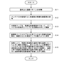
【解決手段】基材上に回路パターンを印刷し(S1)、当該回路パターンの端子上に熱硬化性接着剤を塗布し(S2)、熱硬化性接着剤が塗布された各端子に対応させて半導体チップを載置させ(S3)、加熱温度で膨張する膨張性マイクロカプセルが充てんされている熱硬化性樹脂を、半導体チップを覆うように塗布し(S4)、上記各工程からの搬送状態を維持しつつ、熱硬化性樹脂に対して加熱し、充てんされている膨張性マイクロカプセルを膨張させることで半導体チップのバンプの端子間への押圧力を得て電気的に接続させる(S5)構成とする。
【選択図】図2
Description
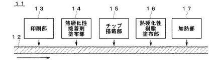
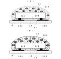
12 連続状基材
13 印刷部
14 熱硬化性接着剤塗布部
15 チップ搭載部
16 熱硬化性樹脂塗布部
17 加熱部
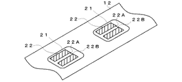
21 回路パターン形成領域
22 アンテナ部
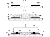
22A,22B 端子
31 第1樹脂材
32 半導体チップ
33 第2樹脂材
33A 膨張性マイクロカプセル
Claims (2)
- 搬送される基材の、当該基材上に形成される回路パターンの所定の端子間に半導体チップのバンプを電気的に接続させる半導体チップの実装方法であって、
前記回路パターンの各端子上に熱硬化性接着剤を塗布する工程と、
前記熱硬化性接着剤が塗布された前記各端子に対応させて半導体チップを載置させる工程と、
加熱温度で膨張する膨張性マイクロカプセルが充てんされている熱硬化性樹脂を、前記半導体チップを覆うように塗布する工程と、
前記各工程からの搬送状態を維持しつつ、少なくとも前記熱硬化性樹脂に対して加熱し、充てんされている前記膨張性マイクロカプセルを膨張させることで前記半導体チップのバンプの端子間への押圧力を得て電気的に接続させる工程と、
を含むことを特徴とする半導体チップの実装方法。 - 請求項1記載の半導体チップの実装方法であって、前記回路パターンの端子間に塗布される熱硬化性接着剤は、加熱により収縮しながら硬化する接着剤であることを特徴とする半導体チップの実装方法。
Priority Applications (1)
| Application Number | Priority Date | Filing Date | Title |
|---|---|---|---|
| JP2008319017A JP5253127B2 (ja) | 2008-12-15 | 2008-12-15 | 半導体チップの実装方法 |
Applications Claiming Priority (1)
| Application Number | Priority Date | Filing Date | Title |
|---|---|---|---|
| JP2008319017A JP5253127B2 (ja) | 2008-12-15 | 2008-12-15 | 半導体チップの実装方法 |
Publications (2)
| Publication Number | Publication Date |
|---|---|
| JP2010141275A true JP2010141275A (ja) | 2010-06-24 |
| JP5253127B2 JP5253127B2 (ja) | 2013-07-31 |
Family
ID=42351110
Family Applications (1)
| Application Number | Title | Priority Date | Filing Date |
|---|---|---|---|
| JP2008319017A Expired - Fee Related JP5253127B2 (ja) | 2008-12-15 | 2008-12-15 | 半導体チップの実装方法 |
Country Status (1)
| Country | Link |
|---|---|
| JP (1) | JP5253127B2 (ja) |
Cited By (1)
| Publication number | Priority date | Publication date | Assignee | Title |
|---|---|---|---|---|
| CN102332413A (zh) * | 2010-12-22 | 2012-01-25 | 傅华贵 | 一种smt锡膏链接工艺 |
Citations (3)
| Publication number | Priority date | Publication date | Assignee | Title |
|---|---|---|---|---|
| JPS6285436A (ja) * | 1985-10-09 | 1987-04-18 | Sharp Corp | 半導体チツプの基板取付方法 |
| JP2002110734A (ja) * | 2000-09-26 | 2002-04-12 | Sony Corp | 部品実装方法及び部品実装モジュール |
| JP2005309953A (ja) * | 2004-04-23 | 2005-11-04 | Dainippon Printing Co Ltd | インターポーザ付シートの巻体およびicタグ |
-
2008
- 2008-12-15 JP JP2008319017A patent/JP5253127B2/ja not_active Expired - Fee Related
Patent Citations (3)
| Publication number | Priority date | Publication date | Assignee | Title |
|---|---|---|---|---|
| JPS6285436A (ja) * | 1985-10-09 | 1987-04-18 | Sharp Corp | 半導体チツプの基板取付方法 |
| JP2002110734A (ja) * | 2000-09-26 | 2002-04-12 | Sony Corp | 部品実装方法及び部品実装モジュール |
| JP2005309953A (ja) * | 2004-04-23 | 2005-11-04 | Dainippon Printing Co Ltd | インターポーザ付シートの巻体およびicタグ |
Cited By (1)
| Publication number | Priority date | Publication date | Assignee | Title |
|---|---|---|---|---|
| CN102332413A (zh) * | 2010-12-22 | 2012-01-25 | 傅华贵 | 一种smt锡膏链接工艺 |
Also Published As
| Publication number | Publication date |
|---|---|
| JP5253127B2 (ja) | 2013-07-31 |
Similar Documents
| Publication | Publication Date | Title |
|---|---|---|
| KR100816107B1 (ko) | Rfid 태그의 제조 방법, 및 rfid 태그 | |
| JP2000311233A (ja) | 回路チップコネクタおよび回路チップを結合する方法 | |
| US20040026033A1 (en) | High speed flip chip assembly process | |
| KR100858979B1 (ko) | 스마트 라벨 인렛 웹 제조를 위한 방법 및 장치 | |
| US20120018084A1 (en) | Printed Circuit Board Assembly Manufacturing Device And Method | |
| US7122087B2 (en) | Method of manufacturing RFID | |
| KR20070039495A (ko) | 전기장치의 고밀도 본딩 | |
| JPH08230367A (ja) | 非接触型icカードならびにその製造方法および装置 | |
| EP2053647A2 (en) | Semiconductor chip mounting method, semiconductor mounting wiring board producing method and semiconductor mounting wiring board | |
| JP2021140670A (ja) | Rfidインレイの製造方法 | |
| CA2628566C (en) | In-mold chip attach | |
| JP5253127B2 (ja) | 半導体チップの実装方法 | |
| JP2008209961A (ja) | 電子装置の製造方法、電子装置が実装された電子機器の製造方法、および、電子装置が装着された物品の製造方法 | |
| JP4860494B2 (ja) | 電子装置の製造方法 | |
| JP2004514291A (ja) | シリコンチップ上の集積回路のスマートラベルへの取付け方法 | |
| US7431218B2 (en) | RFID tag, module component, and RFID tag fabrication method | |
| US7682871B2 (en) | Method for forming a joint | |
| MX2008012339A (es) | Metodos para sujetar un montaje de circuito integrado de un chip invertido a un sustrato. | |
| KR100867954B1 (ko) | 전자소자 내장 인쇄회로기판 및 그 제조방법 | |
| JP2003347359A (ja) | ドライバic圧着装置および圧着方法 | |
| CN100593364C (zh) | 电子器件及其制造方法 | |
| KR100828971B1 (ko) | 자외선을 이용한 투명기판 상의 칩 또는 스트랩 실장방법 | |
| JP3979797B2 (ja) | 電子部品実装済部品の製造方法、電子部品実装済完成品の製造方法、及び半導体部品実装済完成品 | |
| CN101156235A (zh) | 在芯片接触表面和天线接触表面之间建立电连接和机械连接的方法及应答器 | |
| KR20130035733A (ko) | 리플로우 장치 및 이를 이용한 솔더 범프 형성 방법 |
Legal Events
| Date | Code | Title | Description |
|---|---|---|---|
| A621 | Written request for application examination |
Free format text: JAPANESE INTERMEDIATE CODE: A621 Effective date: 20111205 |
|
| A977 | Report on retrieval |
Free format text: JAPANESE INTERMEDIATE CODE: A971007 Effective date: 20121130 |
|
| A131 | Notification of reasons for refusal |
Free format text: JAPANESE INTERMEDIATE CODE: A131 Effective date: 20121204 |
|
| A521 | Request for written amendment filed |
Free format text: JAPANESE INTERMEDIATE CODE: A523 Effective date: 20130116 |
|
| TRDD | Decision of grant or rejection written | ||
| A01 | Written decision to grant a patent or to grant a registration (utility model) |
Free format text: JAPANESE INTERMEDIATE CODE: A01 Effective date: 20130416 |
|
| A61 | First payment of annual fees (during grant procedure) |
Free format text: JAPANESE INTERMEDIATE CODE: A61 Effective date: 20130416 |
|
| R150 | Certificate of patent or registration of utility model |
Free format text: JAPANESE INTERMEDIATE CODE: R150 Ref document number: 5253127 Country of ref document: JP Free format text: JAPANESE INTERMEDIATE CODE: R150 |
|
| FPAY | Renewal fee payment (event date is renewal date of database) |
Free format text: PAYMENT UNTIL: 20160426 Year of fee payment: 3 |
|
| R250 | Receipt of annual fees |
Free format text: JAPANESE INTERMEDIATE CODE: R250 |
|
| R250 | Receipt of annual fees |
Free format text: JAPANESE INTERMEDIATE CODE: R250 |
|
| R250 | Receipt of annual fees |
Free format text: JAPANESE INTERMEDIATE CODE: R250 |
|
| R250 | Receipt of annual fees |
Free format text: JAPANESE INTERMEDIATE CODE: R250 |
|
| R250 | Receipt of annual fees |
Free format text: JAPANESE INTERMEDIATE CODE: R250 |
|
| R250 | Receipt of annual fees |
Free format text: JAPANESE INTERMEDIATE CODE: R250 |
|
| R250 | Receipt of annual fees |
Free format text: JAPANESE INTERMEDIATE CODE: R250 |
|
| R250 | Receipt of annual fees |
Free format text: JAPANESE INTERMEDIATE CODE: R250 |
|
| S533 | Written request for registration of change of name |
Free format text: JAPANESE INTERMEDIATE CODE: R313533 |
|
| R350 | Written notification of registration of transfer |
Free format text: JAPANESE INTERMEDIATE CODE: R350 |
|
| S111 | Request for change of ownership or part of ownership |
Free format text: JAPANESE INTERMEDIATE CODE: R313113 |
|
| R350 | Written notification of registration of transfer |
Free format text: JAPANESE INTERMEDIATE CODE: R350 |
|
| R250 | Receipt of annual fees |
Free format text: JAPANESE INTERMEDIATE CODE: R250 |
|
| LAPS | Cancellation because of no payment of annual fees |