JP2010141278A - Polysaccharide wiring board and method of manufacturing the same - Google Patents
Polysaccharide wiring board and method of manufacturing the same Download PDFInfo
- Publication number
- JP2010141278A JP2010141278A JP2008335999A JP2008335999A JP2010141278A JP 2010141278 A JP2010141278 A JP 2010141278A JP 2008335999 A JP2008335999 A JP 2008335999A JP 2008335999 A JP2008335999 A JP 2008335999A JP 2010141278 A JP2010141278 A JP 2010141278A
- Authority
- JP
- Japan
- Prior art keywords
- wiring
- polysaccharide
- wiring board
- substrate
- skin
- Prior art date
- Legal status (The legal status is an assumption and is not a legal conclusion. Google has not performed a legal analysis and makes no representation as to the accuracy of the status listed.)
- Pending
Links
- 150000004676 glycans Chemical class 0.000 title claims abstract description 223
- 229920001282 polysaccharide Polymers 0.000 title claims abstract description 223
- 239000005017 polysaccharide Substances 0.000 title claims abstract description 223
- 238000004519 manufacturing process Methods 0.000 title claims abstract description 58
- 239000007864 aqueous solution Substances 0.000 claims abstract description 46
- 239000000758 substrate Substances 0.000 claims description 159
- 229920001218 Pullulan Polymers 0.000 claims description 62
- 239000004373 Pullulan Substances 0.000 claims description 62
- 235000019423 pullulan Nutrition 0.000 claims description 62
- KIUKXJAPPMFGSW-DNGZLQJQSA-N (2S,3S,4S,5R,6R)-6-[(2S,3R,4R,5S,6R)-3-Acetamido-2-[(2S,3S,4R,5R,6R)-6-[(2R,3R,4R,5S,6R)-3-acetamido-2,5-dihydroxy-6-(hydroxymethyl)oxan-4-yl]oxy-2-carboxy-4,5-dihydroxyoxan-3-yl]oxy-5-hydroxy-6-(hydroxymethyl)oxan-4-yl]oxy-3,4,5-trihydroxyoxane-2-carboxylic acid Chemical compound CC(=O)N[C@H]1[C@H](O)O[C@H](CO)[C@@H](O)[C@@H]1O[C@H]1[C@H](O)[C@@H](O)[C@H](O[C@H]2[C@@H]([C@@H](O[C@H]3[C@@H]([C@@H](O)[C@H](O)[C@H](O3)C(O)=O)O)[C@H](O)[C@@H](CO)O2)NC(C)=O)[C@@H](C(O)=O)O1 KIUKXJAPPMFGSW-DNGZLQJQSA-N 0.000 claims description 21
- 229920002674 hyaluronan Polymers 0.000 claims description 21
- 229960003160 hyaluronic acid Drugs 0.000 claims description 21
- 230000002209 hydrophobic effect Effects 0.000 claims description 16
- 238000010438 heat treatment Methods 0.000 claims description 14
- 239000012212 insulator Substances 0.000 claims description 14
- 238000009736 wetting Methods 0.000 claims description 14
- 229920002134 Carboxymethyl cellulose Polymers 0.000 claims description 12
- 229920002472 Starch Polymers 0.000 claims description 12
- 239000001768 carboxy methyl cellulose Substances 0.000 claims description 12
- 235000010948 carboxy methyl cellulose Nutrition 0.000 claims description 12
- 239000008112 carboxymethyl-cellulose Substances 0.000 claims description 12
- 230000005236 sound signal Effects 0.000 claims description 12
- 239000008107 starch Substances 0.000 claims description 12
- 235000019698 starch Nutrition 0.000 claims description 12
- 238000001035 drying Methods 0.000 claims description 11
- 238000000034 method Methods 0.000 abstract description 29
- 239000000463 material Substances 0.000 abstract description 19
- 229920005989 resin Polymers 0.000 abstract description 12
- 239000011347 resin Substances 0.000 abstract description 12
- 239000002699 waste material Substances 0.000 abstract description 8
- 230000007613 environmental effect Effects 0.000 abstract description 7
- 239000000126 substance Substances 0.000 abstract description 6
- 238000003912 environmental pollution Methods 0.000 abstract description 4
- 239000000243 solution Substances 0.000 abstract description 4
- 230000008929 regeneration Effects 0.000 abstract 1
- 238000011069 regeneration method Methods 0.000 abstract 1
- 230000001070 adhesive effect Effects 0.000 description 32
- 239000000853 adhesive Substances 0.000 description 30
- 238000012360 testing method Methods 0.000 description 22
- XLYOFNOQVPJJNP-UHFFFAOYSA-N water Substances O XLYOFNOQVPJJNP-UHFFFAOYSA-N 0.000 description 22
- 239000002994 raw material Substances 0.000 description 21
- 239000003990 capacitor Substances 0.000 description 16
- 239000000047 product Substances 0.000 description 15
- 238000009429 electrical wiring Methods 0.000 description 14
- 238000005516 engineering process Methods 0.000 description 14
- 238000009413 insulation Methods 0.000 description 14
- 238000005259 measurement Methods 0.000 description 13
- 230000003287 optical effect Effects 0.000 description 12
- 229910052782 aluminium Inorganic materials 0.000 description 11
- XAGFODPZIPBFFR-UHFFFAOYSA-N aluminium Chemical compound [Al] XAGFODPZIPBFFR-UHFFFAOYSA-N 0.000 description 11
- 230000000694 effects Effects 0.000 description 11
- 229910001220 stainless steel Inorganic materials 0.000 description 11
- 239000010935 stainless steel Substances 0.000 description 11
- 239000000919 ceramic Substances 0.000 description 8
- RTAQQCXQSZGOHL-UHFFFAOYSA-N Titanium Chemical compound [Ti] RTAQQCXQSZGOHL-UHFFFAOYSA-N 0.000 description 7
- 238000005266 casting Methods 0.000 description 7
- RYGMFSIKBFXOCR-UHFFFAOYSA-N Copper Chemical compound [Cu] RYGMFSIKBFXOCR-UHFFFAOYSA-N 0.000 description 6
- XEEYBQQBJWHFJM-UHFFFAOYSA-N Iron Chemical compound [Fe] XEEYBQQBJWHFJM-UHFFFAOYSA-N 0.000 description 6
- 210000000988 bone and bone Anatomy 0.000 description 6
- 229910052802 copper Inorganic materials 0.000 description 6
- 239000010949 copper Substances 0.000 description 6
- 230000006870 function Effects 0.000 description 6
- 239000010410 layer Substances 0.000 description 6
- 229910052719 titanium Inorganic materials 0.000 description 6
- 239000010936 titanium Substances 0.000 description 6
- 238000001771 vacuum deposition Methods 0.000 description 6
- BQCADISMDOOEFD-UHFFFAOYSA-N Silver Chemical compound [Ag] BQCADISMDOOEFD-UHFFFAOYSA-N 0.000 description 5
- 230000008569 process Effects 0.000 description 5
- 238000000465 moulding Methods 0.000 description 4
- BASFCYQUMIYNBI-UHFFFAOYSA-N platinum Chemical compound [Pt] BASFCYQUMIYNBI-UHFFFAOYSA-N 0.000 description 4
- 208000010201 Exanthema Diseases 0.000 description 3
- 230000005540 biological transmission Effects 0.000 description 3
- 238000011161 development Methods 0.000 description 3
- 230000005611 electricity Effects 0.000 description 3
- 201000005884 exanthem Diseases 0.000 description 3
- 229910052742 iron Inorganic materials 0.000 description 3
- 239000000696 magnetic material Substances 0.000 description 3
- 239000013307 optical fiber Substances 0.000 description 3
- 238000002360 preparation method Methods 0.000 description 3
- 206010037844 rash Diseases 0.000 description 3
- 238000004064 recycling Methods 0.000 description 3
- 239000002356 single layer Substances 0.000 description 3
- 230000035900 sweating Effects 0.000 description 3
- 206010040880 Skin irritation Diseases 0.000 description 2
- 238000006243 chemical reaction Methods 0.000 description 2
- 239000000835 fiber Substances 0.000 description 2
- 239000007789 gas Substances 0.000 description 2
- 239000011521 glass Substances 0.000 description 2
- PCHJSUWPFVWCPO-UHFFFAOYSA-N gold Chemical compound [Au] PCHJSUWPFVWCPO-UHFFFAOYSA-N 0.000 description 2
- 229910052737 gold Inorganic materials 0.000 description 2
- 239000010931 gold Substances 0.000 description 2
- 230000017525 heat dissipation Effects 0.000 description 2
- 239000000543 intermediate Substances 0.000 description 2
- 230000001678 irradiating effect Effects 0.000 description 2
- 230000007774 longterm Effects 0.000 description 2
- 229910052751 metal Inorganic materials 0.000 description 2
- 239000002184 metal Substances 0.000 description 2
- 239000003208 petroleum Substances 0.000 description 2
- 229910052697 platinum Inorganic materials 0.000 description 2
- 238000012545 processing Methods 0.000 description 2
- 229910052709 silver Inorganic materials 0.000 description 2
- 239000004332 silver Substances 0.000 description 2
- 230000036556 skin irritation Effects 0.000 description 2
- 231100000475 skin irritation Toxicity 0.000 description 2
- 229910000679 solder Inorganic materials 0.000 description 2
- 238000007711 solidification Methods 0.000 description 2
- 230000008023 solidification Effects 0.000 description 2
- 239000002904 solvent Substances 0.000 description 2
- 229920000936 Agarose Polymers 0.000 description 1
- 229920001342 Bakelite® Polymers 0.000 description 1
- 229920002101 Chitin Polymers 0.000 description 1
- 239000004593 Epoxy Substances 0.000 description 1
- 229920002527 Glycogen Polymers 0.000 description 1
- HTTJABKRGRZYRN-UHFFFAOYSA-N Heparin Chemical compound OC1C(NC(=O)C)C(O)OC(COS(O)(=O)=O)C1OC1C(OS(O)(=O)=O)C(O)C(OC2C(C(OS(O)(=O)=O)C(OC3C(C(O)C(O)C(O3)C(O)=O)OS(O)(=O)=O)C(CO)O2)NS(O)(=O)=O)C(C(O)=O)O1 HTTJABKRGRZYRN-UHFFFAOYSA-N 0.000 description 1
- 206010061218 Inflammation Diseases 0.000 description 1
- XUIMIQQOPSSXEZ-UHFFFAOYSA-N Silicon Chemical compound [Si] XUIMIQQOPSSXEZ-UHFFFAOYSA-N 0.000 description 1
- 229920002000 Xyloglucan Polymers 0.000 description 1
- 239000012790 adhesive layer Substances 0.000 description 1
- 239000004637 bakelite Substances 0.000 description 1
- 230000008901 benefit Effects 0.000 description 1
- 239000012620 biological material Substances 0.000 description 1
- 239000000679 carrageenan Substances 0.000 description 1
- 229920001525 carrageenan Polymers 0.000 description 1
- 235000010418 carrageenan Nutrition 0.000 description 1
- 229940113118 carrageenan Drugs 0.000 description 1
- 230000015556 catabolic process Effects 0.000 description 1
- 229920002678 cellulose Polymers 0.000 description 1
- 239000001913 cellulose Substances 0.000 description 1
- 239000013065 commercial product Substances 0.000 description 1
- 238000012790 confirmation Methods 0.000 description 1
- 239000000470 constituent Substances 0.000 description 1
- 238000006731 degradation reaction Methods 0.000 description 1
- 230000006866 deterioration Effects 0.000 description 1
- 238000010586 diagram Methods 0.000 description 1
- 238000007598 dipping method Methods 0.000 description 1
- 210000000613 ear canal Anatomy 0.000 description 1
- 230000005670 electromagnetic radiation Effects 0.000 description 1
- 125000003700 epoxy group Chemical group 0.000 description 1
- 229940096919 glycogen Drugs 0.000 description 1
- 230000036541 health Effects 0.000 description 1
- 229920000669 heparin Polymers 0.000 description 1
- 229960002897 heparin Drugs 0.000 description 1
- 230000006698 induction Effects 0.000 description 1
- 230000004054 inflammatory process Effects 0.000 description 1
- 238000003780 insertion Methods 0.000 description 1
- 230000037431 insertion Effects 0.000 description 1
- 230000010354 integration Effects 0.000 description 1
- 239000012778 molding material Substances 0.000 description 1
- 239000001814 pectin Substances 0.000 description 1
- 229920001277 pectin Polymers 0.000 description 1
- 235000010987 pectin Nutrition 0.000 description 1
- 229920000647 polyepoxide Polymers 0.000 description 1
- 239000010970 precious metal Substances 0.000 description 1
- 238000007639 printing Methods 0.000 description 1
- 230000001681 protective effect Effects 0.000 description 1
- 238000012827 research and development Methods 0.000 description 1
- 239000010703 silicon Substances 0.000 description 1
- 229910052710 silicon Inorganic materials 0.000 description 1
- UHVMMEOXYDMDKI-JKYCWFKZSA-L zinc;1-(5-cyanopyridin-2-yl)-3-[(1s,2s)-2-(6-fluoro-2-hydroxy-3-propanoylphenyl)cyclopropyl]urea;diacetate Chemical compound [Zn+2].CC([O-])=O.CC([O-])=O.CCC(=O)C1=CC=C(F)C([C@H]2[C@H](C2)NC(=O)NC=2N=CC(=CC=2)C#N)=C1O UHVMMEOXYDMDKI-JKYCWFKZSA-L 0.000 description 1
Images


Landscapes
- Production Of Multi-Layered Print Wiring Board (AREA)
Abstract
Description
本発明は、基板表面に配置された表面配線及び/又は基板内部に配置された埋め込み配線を有し、かつそれらの配線が電気部品や電子部品に結線可能な配線である多糖質配線基板の技術、及びその配線基板製造技術に関するものであり、さらには多糖質からなら絶縁体により前記基板及び前記部品が封入された前記多糖質配線基板の技術に関するものである。 The present invention relates to a polysaccharide wiring board technology that has surface wiring arranged on the surface of the substrate and / or embedded wiring arranged inside the substrate, and these wirings are wiring that can be connected to an electrical component or an electronic component. Further, the present invention relates to a technique for manufacturing the polysaccharide wiring board, and more particularly, to a technique for the polysaccharide wiring board in which the substrate and the components are sealed with an insulator.
また、本発明は、基板表面に露呈された表面電極や微細針電極を有した、皮膚装着可能な多糖質配線基板の技術に関するものであり、また、基板表面に磁気コイル配線及び磁性体を有した、皮膚装着可能なスピーカを搭載した多糖質配線基板の技術に関するものであり、さらには基板表面に配置された発光ダイオード及び/又は基板内部に埋め込み配置された発光ダイオードを有した、皮膚装着可能な発光ダイオードを搭載した多糖質配線基板の技術に関するものである。 The present invention also relates to a technique for a polysaccharide-wiring board that can be attached to the skin, having surface electrodes and fine needle electrodes exposed on the surface of the board, and has a magnetic coil wiring and a magnetic body on the board surface. Further, the present invention relates to a polysaccharide wiring board technology equipped with a speaker that can be worn on the skin, and further includes a light-emitting diode arranged on the surface of the board and / or a light-emitting diode embedded inside the board, and can be worn on the skin. The present invention relates to a polysaccharide wiring board technology equipped with a simple light emitting diode.
他方、電気部品や電子部品を集積回路として搭載する配線基板においては、集積回路を安定作動させるべく、基板材料として前述の諸々の特性等を考慮して主に樹脂(ベークライト、エポキシなど)が使用されたり、また放熱性を特に重視する場合にはセラミックスが使用されたりしてきた。例えば、特許文献1では電気配線基板用基材が提供され、ここでは不要な電磁波放射の問題を解決すべく、基板材料として樹脂やセラミックスを使用した発明が開示されている。
また、生体の電気的計測に関する技術分野では、身体に電気回路をなす計測用電極を装着する必要があるが、特に心電図計測や脳波計測においては、電極を安定に皮膚装着し、かつ皮膚との電気的接触を安定にする為、吸盤や導電性の銀ペーストを用いることにより皮膚装着を行ってきた。しかしながら、一般に配線回路基板である電極を身体装着する場合には、主として基板材料が樹脂やセラミックスである為、これら材料を皮膚装着するには適度な粘着性を有した接着剤を要することとなる。例えば、特許文献2では皮膚に貼用される健康増進具が提供され、ここでは電極を皮膚装着する際に使用する接着剤として皮膚粘着剤層を使用した発明が開示されている。
電気部品や電子部品を集積回路として搭載する配線基板の主成分である樹脂については、いずれかの部品の寿命が尽きた時点で必然的に廃棄物となり、寿命のある電気部品や電子部品まで含めて廃棄され、ここでも資源浪費の問題が存することとなった。これらの配線基板の処理には一般廃棄や焼却が行われてきたが、前述と同様に有害な廃棄物からの有害物質の飛散や有害な排出ガスの発生などが大きな環境問題となっていた。さらには、電子部品の高集積化の為に使用する放熱性のよいセラミックス基板についても、いずれかの部品の寿命が尽きた時点で廃棄物として扱われてきたが、その処理には主に埋立地等への一般廃棄が行われてきており、このことは後世に環境汚染問題となる可能性を孕むこととなる。かかる配線基板の処理現場においては、電気部品や電子部品を搭載する樹脂やセラミックス等の配線基板から、ハンダによって取り付けられている部品を破壊することなく取り外すことが不可能である為、それらの部品を再生して使用することも不可能であり、実際にはそれらの部品あるいは基板に使用された配線用の貴金属しか再生利用できなかったり、またコネクタに差し込んだ、取り外しの容易な一部の部品のみ再生使用が可能であったりして、配線基板で使用されている部品全体から見ればその再生割合は低いという点で大きな問題であった。 Resin, which is the main component of a wiring board on which electrical and electronic components are mounted as an integrated circuit, will inevitably become waste when one of its components has reached the end of its life. The problem of waste of resources still existed here. Although general disposal and incineration have been carried out for the processing of these wiring boards, scattering of harmful substances from harmful wastes and generation of harmful exhaust gases have become major environmental problems as described above. Furthermore, ceramic substrates with good heat dissipation used for high integration of electronic components have been treated as waste when any component has reached the end of their life. General disposal to the ground etc. has been carried out, and this entails the possibility of becoming an environmental pollution problem in future generations. In the processing site of such wiring boards, it is impossible to remove the parts attached by solder from the wiring boards made of resin or ceramics on which electric parts and electronic parts are mounted without destroying them. It is also impossible to recycle and use, and in fact, only those precious metals used for wiring on those parts or boards can be recycled, or some parts that are easily removed can be inserted into connectors. This is a big problem in that the recycling ratio is low when viewed from the whole parts used in the wiring board.
以上の諸問題を考慮して、ハンダによって樹脂基板に搭載された再利用可能な電気部品や電子部品を取外して再生することは不可能である為、微視的には部品再生技術の開発、さらに巨視的には地球規模における資源継続性を主目的とした永久技術(Eternal Technology)の開発が重要課題となっていた。 Considering the above problems, it is impossible to remove and recycle reusable electrical and electronic components mounted on resin substrates by solder. Furthermore, macroscopically, the development of a permanent technology (Eternal Technology) whose main purpose is resource continuity on a global scale has become an important issue.
他方、表面配線や埋め込み配線を有する多層配線基板を製作する工程においては、初めに通常の表面配線を設ける基板を製作した後、その表面配線を埋め込むように覆う新たな基板を設け、その新たな基板上にさらに表面配線を設けると2層配線が製作できる。この工程を繰り返すことにより配線の多層化が可能となるが、このように従来の多層配線基板の製作では、各層の製作及びその配線工程を繰り返すことが必要であり、このことがコスト高の要因となっており、製造技術における大きな課題となっていた。従って、表面配線や埋め込み配線を有する配線基板の製造において簡便かつ低コストの製造技術の開発が求められていた。 On the other hand, in the process of manufacturing the multilayer wiring board having the surface wiring and the embedded wiring, first, after manufacturing the substrate on which the normal surface wiring is provided, a new substrate is provided to cover the surface wiring so as to be embedded. If a surface wiring is further provided on the substrate, a two-layer wiring can be manufactured. By repeating this process, it is possible to make the wiring multi-layered. However, in the production of the conventional multilayer wiring board as described above, it is necessary to repeat the production of each layer and the wiring process, which is a factor of high cost. It has become a major issue in manufacturing technology. Accordingly, there has been a demand for development of a simple and low-cost manufacturing technique in the manufacture of a wiring board having surface wiring and embedded wiring.
また、生体の電気的計測においては身体に計測用電極を装着することになるが、配線回路基板である電極を装着する場合、主に樹脂基板やセラミックス基板を身体へ装着するには接着剤を必要とする為、接着剤による皮膚表面のかぶれや発汗による粘着剤の性能低下等に起因して長時間の基板装着、すなわち電極装着の使用が不可能となる問題があった。従って、一昼夜以上の長期間を通して計測する心電計や脳波計の電極の装着には前述の問題が伴っていた。さらに心電図計測や脳波計測においては、電極を安定に皮膚装着し、かつ皮膚との電気的接触を安定にする為に、電極直径の拡大化、接着機能として吸盤や導電性の銀ペーストの使用等を行ってきたが、皮膚感触として違和感や冷たさの為に被験者に不快感を与えたり、前述の皮膚かぶれや発汗による接着機能が低下したりするという点が問題であった。これらの諸問題を解決するべく、不快感が少なく、かつ簡便な、計測用電極の身体装着技術の開発が課題となっていた。 In addition, measurement electrodes are attached to the body for electrical measurement of living organisms, but when attaching electrodes that are printed circuit boards, adhesives are mainly used to attach resin substrates and ceramic substrates to the body. Since it is necessary, there has been a problem that it is impossible to use the substrate for a long time, that is, the electrode mounting due to the rash on the skin surface due to the adhesive or the performance degradation of the adhesive due to perspiration. Therefore, the above-mentioned problems have been associated with the attachment of electrocardiographs and electroencephalograph electrodes that are measured over a long period of time, more than one day. Furthermore, in electrocardiogram measurement and electroencephalogram measurement, in order to stably attach the electrode to the skin and stabilize the electrical contact with the skin, the electrode diameter is enlarged, the use of a suction cup or conductive silver paste as an adhesive function, etc. However, there are problems in that the subject feels uncomfortable because of the skin feel and the coldness, and the adhesion function due to the above-mentioned skin irritation and perspiration is reduced. In order to solve these problems, there has been a problem of developing a body-mounted technique for measuring electrodes that is less uncomfortable and simple.
更には、一般に聴覚機能の補助具として使用される補聴器においては、身体を動かす度に補聴器が外れたり、長年の使用により耳穴を痛める等の不便が発生したりする問題や、極度に聴覚能力が衰えた人には効果が極めて低い等の問題があった。それ故、骨伝導型の補聴器が開発されてきているものの、サイズのより小さい、かつ低コストのものが必要とされ、このようなニーズに対して配線基板技術を如何に応用するかが課題となっていた。 Furthermore, in hearing aids that are generally used as hearing aids, there are problems such as the hearing aid being detached each time the body is moved, inconveniences such as hurting the ear canal due to long-term use, and extreme hearing ability. There were problems such as extremely low effectiveness for those who declined. Therefore, although bone conduction type hearing aids have been developed, smaller size and lower cost are required, and how to apply wiring board technology to such needs is a problem. It was.
また、一般に省エネルギー及び長寿命の光発生デバイスとして使用されてきている発光ダイオードにおいては、その技術進歩によりにより光の用途が拡大してきたものの、発光ダイオードの生体への応用としては、前述の発光ダイオードによる光を皮膚に照射するに際しは、光路の素材が従来使用してきたガラスであるため、光ファイバのように光路間を接続する場合は、光軸合せを正確にしないと、散乱のため伝達効率を低下させることとなる。従って、ここでは安定して皮膚に発光ダイオードを装着させ、かつ伝達効率よく皮膚へ光照射するかが問題となってきており、すなわちこの問題に対して配線基板技術を如何に応用するかが重要課題となっていた。 Moreover, in light emitting diodes that have been used as light-generating devices with energy saving and long life, the use of light has been expanded due to technological advancement. When irradiating the skin with light, the material of the optical path is glass that has been used in the past, so when connecting between optical paths like an optical fiber, if the optical axis alignment is not accurate, the transmission efficiency will be due to scattering Will be reduced. Therefore, it has become a problem here to stably attach light emitting diodes to the skin and to irradiate the skin with light efficiently. That is, how to apply the wiring board technology to this problem is important. It was an issue.
以上の諸課題を解決する為に本発明者らは鋭意研究開発を行い、本発明においてこれらの課題を解決するための手段、方法として、
(1)多糖質からなる配線基板において、前記基板表面に配置された表面配線又は前記基板内部に配置された埋め込み配線を有する構造であり、かつ前記配線が電気部品及び/又は電子部品に結線可能な配線であることを特徴とする表面配線又は埋め込み配線を有する多糖質配線基板、並びに、
(2)前記多糖質配線基板における多糖質が、プルラン、カルボキシメチルセルロース、デンプン、ヒアルロン酸、から選択される1の多糖質であることを特徴とする前記(1)記載の表面配線又は埋め込み配線を有する多糖質配線基板、並びに、
(3)前記表面配線を有する構造の多糖質配線基板の製造においては、疎水性を有するモールド内に10重量%〜70重量%の多糖質水溶物を充填した後、前記モールドを湿度10%以下の乾燥大気中に静置することにより、又は前記モールドを50℃〜90℃に加熱することにより、前記モールド内に充填された前記多糖質水溶物を乾燥固形化して成形し、前記成形物の表面に電気部品及び/又は電子部品に結線可能な配線を設けることを特徴とし、又は、前記埋め込み配線を有する構造の多糖質配線基板の製造においては、電気部品及び/又は電子部品に結線可能な配線を、疎水性を有するモールド内に配置し、前記モールド内に10重量%〜70重量%の多糖質水溶物を充填した後、前記モールドを湿度10%以下の乾燥大気中に静置することにより、又は前記モールドを50℃〜90℃に加熱することにより、前記モールド内に充填された前記多糖質水溶物を乾燥固形化して成形することを特徴とする請求項1又は2記載の表面配線又は埋め込み配線を有する多糖質配線基板の製造方法、並びに、
(4)多糖質からなる配線基板において、前記基板表面に配置された表面配線及び前記基板内部に配置された埋め込み配線を有する構造であり、かつ前記配線が電気部品及び/又は電子部品に結線可能な配線であることを特徴とする表面配線及び埋め込み配線を有する多糖質配線基板、並びに、
(5)前記多糖質配線基板における多糖質が、プルラン、カルボキシメチルセルロース、デンプン、ヒアルロン酸、から選択される1の多糖質であることを特徴とする前記(4)記載の表面配線及び埋め込み配線を有する多糖質配線基板、並びに、
(6)電気部品及び/又は電子部品に結線可能な配線を、疎水性を有するモールド内に配置し、前記モールド内に10重量%〜70重量%の多糖質水溶物を充填した後、前記モールドを湿度10%以下の乾燥大気中に静置することにより、又は前記モールドを50℃〜90℃に加熱することにより、前記モールド内に充填された前記多糖質水溶物を乾燥固形化して成形し、さらに前記成形物の表面に電気部品及び/又は電子部品に結線可能な配線を設けることを特徴とする前記(4)又は(5)記載の表面配線及び埋め込み配線を有する多糖質配線基板の製造方法、並びに、
(7)プルラン又はヒアルロン酸からなる絶縁体により、前記基板及び前記部品が封入されたことを特徴とする前記(1)或いは(4)いずれか記載の表面配線又は埋め込み配線、或いは表面配線及び埋め込み配線を有する多糖質配線基板、並びに、
(8)多糖質からなる配線基板において、前記基板内部に配置された埋め込み配線の末端部が前記基板の表面に露呈された表面電極を有する構造であり、かつ前記配線が電気部品及び/又は電子部品に結線可能な配線であり、さらに前記表面電極が露呈された側の基板表面を湿潤させることにより前記基板が皮膚に粘着して前記表面電極が皮膚表面に接触することを特徴とする皮膚装着可能な表面電極を有する多糖質配線基板、並びに、
(9)多糖質からなる配線基板において、前記基板内部に配置された埋め込み配線の末端部と結線され、前記基板の表面に露呈された微細針電極を有する構造であり、かつ前記配線が電気部品及び/又は電子部品に結線可能な配線であり、さらに前記微細針電極が露呈された側の基板表面を湿潤させることにより前記基板が皮膚に粘着して前記微細針電極が皮膚表面に挿入することを特徴とする皮膚装着可能な微細針電極を有する多糖質配線基板、並びに、
(10)多糖質からなる配線基板において、前記基板表面に配置された磁気コイル配線、及び前記磁気コイル配線内に配置された磁性体を有する構造であり、かつ前記磁気コイル配線が電気部品及び/又は電子部品に結線可能な配線であり、さらに前記磁性体が配置された基板表面と反対側の基板表面を湿潤させることにより前記基板が皮膚に粘着し、前記磁気コイル配線に通電して前記磁性体を振動させることによりスピーカとして皮膚内に音声信号を伝導することを特徴とする皮膚装着可能なスピーカを搭載する多糖質配線基板、並びに、
(11)多糖質からなる配線基板において、前記基板表面に配置された表面配線及び/又は前記基板内部に配置された埋め込み配線と結線され、前記基板の表面に配置された発光ダイオード及び/又は前記基板内部に埋め込み配置された発光ダイオードを有する構造であり、かつ前記配線が電気部品及び/又は電子部品に結線可能な配線であり、さらに前記基板表面を湿潤させることにより前記基板が皮膚に粘着し、前記基板の表面に配置された発光ダイオード及び/又は前記基板内部に埋め込み配置された発光ダイオードにより皮膚表面を照光することを特徴とする皮膚装着可能な発光ダイオードを搭載する多糖質配線基板、並びに、
(12)前記多糖質配線基板における多糖質が、プルラン、カルボキシメチルセルロース、デンプン、ヒアルロン酸、から選択される1の多糖質であることを特徴とする前記(8)から(11)いずれか記載の多糖質配線基板、
との発明を成したものである。In order to solve the above problems, the inventors have conducted intensive research and development, and as means and methods for solving these problems in the present invention,
(1) A wiring board made of a polysaccharide has a structure having a surface wiring arranged on the surface of the substrate or a buried wiring arranged inside the substrate, and the wiring can be connected to an electrical component and / or an electronic component. A polysaccharide wiring board having surface wiring or embedded wiring, characterized by
(2) The surface wiring or embedded wiring according to (1) above, wherein the polysaccharide in the polysaccharide wiring board is one polysaccharide selected from pullulan, carboxymethylcellulose, starch, and hyaluronic acid. A polysaccharide wiring board, and
(3) In the production of the polysaccharide wiring board having the structure having the surface wiring, after filling the hydrophobic mold with 10% by weight to 70% by weight of the polysaccharide aqueous solution, the humidity of the mold is 10% or less. The polysaccharide aqueous solution filled in the mold is dried and solidified and molded by standing in a dry atmosphere of the above or by heating the mold to 50 ° C. to 90 ° C. A wiring that can be connected to an electrical component and / or an electronic component is provided on the surface, or in the manufacture of a polysaccharide wiring board having a structure having the embedded wiring, the wiring can be connected to an electrical component and / or an electronic component. The wiring is placed in a hydrophobic mold and filled with 10% to 70% by weight polysaccharide aqueous solution, and then the mold is left in a dry atmosphere with a humidity of 10% or less. 3. The polysaccharide aqueous solution filled in the mold is dried and solidified and molded by heating the mold to 50 ° C. to 90 ° C. Manufacturing method of polysaccharide wiring board having surface wiring or embedded wiring, and
(4) A polysaccharide wiring board having a structure having surface wiring arranged on the substrate surface and embedded wiring arranged inside the board, and the wiring can be connected to an electrical component and / or an electronic component. A polysaccharide wiring board having a surface wiring and an embedded wiring, and
(5) The surface wiring and embedded wiring according to (4) above, wherein the polysaccharide in the polysaccharide wiring board is one polysaccharide selected from pullulan, carboxymethylcellulose, starch, and hyaluronic acid. A polysaccharide wiring board, and
(6) A wiring that can be connected to an electrical component and / or an electronic component is disposed in a hydrophobic mold, and 10% by weight to 70% by weight polysaccharide aqueous solution is filled in the mold, and then the mold is used. By standing in a dry atmosphere with a humidity of 10% or less, or by heating the mold to 50 ° C. to 90 ° C. to dry and solidify the polysaccharide aqueous solution filled in the mold. Furthermore, the manufacturing method of the polysaccharide wiring board having the surface wiring and the embedded wiring according to the above (4) or (5), characterized in that a wiring that can be connected to an electrical component and / or an electronic component is provided on the surface of the molded product. Method, and
(7) The surface wiring or embedded wiring or the surface wiring and embedded according to any one of (1) or (4), wherein the substrate and the component are sealed with an insulator made of pullulan or hyaluronic acid. A polysaccharide wiring board having wiring, and
(8) The polysaccharide wiring board has a structure in which a terminal portion of the embedded wiring disposed inside the substrate has a surface electrode exposed on the surface of the board, and the wiring is an electrical component and / or an electronic device. A skin mounting characterized in that it is a wiring that can be connected to a component, and the substrate is adhered to the skin by wetting the substrate surface on which the surface electrode is exposed, so that the surface electrode contacts the skin surface. Polysaccharide wiring board with possible surface electrodes, and
(9) A wiring board made of a polysaccharide, wherein the wiring board has a structure having a fine needle electrode that is connected to a terminal portion of an embedded wiring disposed inside the substrate and exposed on the surface of the board, and the wiring is an electrical component And / or a wiring that can be connected to an electronic component, and the substrate surface on the side where the fine needle electrode is exposed is wetted so that the substrate adheres to the skin and the fine needle electrode is inserted into the skin surface. A polysaccharide wiring board having fine needle electrodes that can be worn on the skin, and
(10) A wiring board made of a polysaccharide having a structure having a magnetic coil wiring disposed on the surface of the substrate and a magnetic body disposed in the magnetic coil wiring, wherein the magnetic coil wiring is an electrical component and / or Alternatively, the wiring can be connected to an electronic component, and the substrate adheres to the skin by wetting the substrate surface opposite to the substrate surface on which the magnetic body is disposed, and the magnetic coil wiring is energized to pass the magnetic A polysaccharide wiring board equipped with a skin-worn speaker, characterized by conducting an audio signal in the skin as a speaker by vibrating the body, and
(11) In the wiring substrate made of a polysaccharide, the light-emitting diode connected to the surface wiring disposed on the surface of the substrate and / or the embedded wiring disposed inside the substrate, and disposed on the surface of the substrate, and / or It has a structure having a light emitting diode embedded in a substrate, and the wiring is a wiring that can be connected to an electrical component and / or an electronic component, and the substrate adheres to the skin by wetting the surface of the substrate. A polysaccharide wiring board having a light-emitting diode mounted on the surface of the substrate and / or a light-emitting diode embedded in the substrate to illuminate the skin surface, ,
(12) The polysaccharide according to any one of (8) to (11), wherein the polysaccharide in the polysaccharide wiring board is one polysaccharide selected from pullulan, carboxymethylcellulose, starch, and hyaluronic acid. Polysaccharide wiring board,
This invention is made.
本発明の多糖質配線基板においては、多糖質からなる配線基板において、前記基板表面に配置された表面配線及び/又は前記基板内部に配置された埋め込み配線を有する構造であり、かつ前記配線が電気部品及び/又は電子部品に結線可能な配線であるとすることにより、いずれかの部品の寿命が尽きたり、前記の結線可能な配線に支障をきたしたりした時点での廃棄処理は、多糖質の特性である水溶性を活かし、多糖質配線基板を適当量の水中に水溶させることで対応できる。これにより、埋立地等への廃棄や高熱炉による焼却を必要とせず、廃棄物からの有害物質の飛散や有害な排出ガスの発生などの環境問題は発生しないこととなる。さらには、水溶した多糖質配線基板を含む水中から再使用可能な電気部品や電子部品を容易に、かつ低コストで回収することができ、本発明の多糖質配線基板を水溶処理することにより、有用な部品再生技術へと展開し得る。また、電気部品あるいは電子部品をコネクタで接続し、取り付ける基板の素材および覆う保護絶縁体の素材を多糖質で製作すると、容易に水溶させることができ、部品および回路部みの取り出せるようになるので、各部品を破壊なくコネクタから外すことができるので、電気部品および電子部品すべてを永久使用する目処をつけることができる、すなわち、本発明は部品再生技術へと展開でき、さらには永久技術へと発展し得るものである。また、本発明の多糖質配線基板の製造においては、生物由来材料である多糖質原料を使用するので、その製造プロセスでは石油系原料や様々な化学物質中間体及びそれらの化学反応、また溶剤をも介在せず、樹脂やセラミックスを原料にする場合と比べて資源の消費、環境汚染等の環境負荷が極めて小さく、地球に優しい原料である多糖質を使用した簡便かつ低コストの配線基板製造技術であることとなる。 In the polysaccharide wiring board of the present invention, the polysaccharide wiring board has a structure having a surface wiring disposed on the surface of the substrate and / or a buried wiring disposed inside the substrate, and the wiring is electrically connected. By disposing wiring that can be connected to a component and / or electronic component, the disposal process at the time when the life of any of the components has expired or the wiring that can be connected is hindered is not possible. Taking advantage of the water-solubility, which is a characteristic, it can be handled by dissolving the polysaccharide wiring board in an appropriate amount of water. This eliminates the need for disposal in landfills or incineration using a high-temperature furnace, and does not cause environmental problems such as scattering of harmful substances from waste and generation of harmful exhaust gases. Furthermore, it is possible to easily and inexpensively collect reusable electrical components and electronic components from the water containing the water-soluble polysaccharide wiring board, and by subjecting the polysaccharide wiring board of the present invention to water treatment, It can be developed into useful parts recycling technology. In addition, if electrical components or electronic components are connected with connectors, and the substrate material to be attached and the protective insulator material to be manufactured are made of polysaccharides, they can be easily dissolved in water and the components and circuit parts can be removed. Since each component can be removed from the connector without breaking, all electrical and electronic components can be used permanently. That is, the present invention can be developed into a component recycling technology, and further into a permanent technology. It can develop. Moreover, since the polysaccharide raw material which is a biological material is used in the manufacture of the polysaccharide wiring board of the present invention, petroleum-based raw materials, various chemical intermediates and their chemical reactions, and solvents are used in the manufacturing process. Simple and low-cost wiring board manufacturing technology using polysaccharides, which are environmentally friendly raw materials, with less environmental impacts such as resource consumption and environmental pollution compared to resin and ceramics as raw materials. It will be.
本発明の皮膚装着可能な表面電極又は微細針電極を有する多糖質配線基板においては、多糖質からなる配線基板において、前記基板内部に配置された埋め込み配線の末端部が前記基板の表面に露呈された表面電極、又は前記基板内部に配置された埋め込み配線の末端部と結線され、前記基板の表面に露呈された微細針電極、を有する構造であり、かつ前記配線が電気部品及び/又は電子部品に結線可能な配線であり、さらに前記表面電極又は前記微細針電極が露呈された側の基板表面を湿潤させることにより前記基板が皮膚に粘着して前記表面電極又は前記微細針電極が皮膚表面に接触又は挿入することにより、接着剤による皮膚表面のかぶれや発汗による粘着剤の性能低下等に起因した長時間の基板装着、すなわち電極の装着使用が不可能となる問題を克服することとなった。さらに、心電図計測や脳波計測のように身体内部からの電気信号を捉える場合、皮膚表面の電位の計測あるいは皮膚表面から電流を導入するように電気部品あるいは電子部品を搭載した配線基板および表面電極を皮膚表面に設ける必要があるが、配線基板の素材を多糖質にすることによって、裏面を湿気させて皮膚に粘着させて装着させるので、皮膚表面のかぶれ等の炎症もなく、長期に渡る計測が可能となる。また、微細針電極を採用すると、皮膚内に微細針電極の先端を挿入することができ、電気接触抵抗を極力低減させることができ、電気接触抵抗を押させるために吸盤を持たせたり、電極の直径を大きくしたり、導電性の銀ペーストによって皮膚に付着させたりする必要がなく、極めて小さい電極を使用することできるので、使用感において違和感を抑えることができる。このように、本発明の皮膚装着可能な表面電極又は微細針電極を有する多糖質配線基板により、前述の従来技術における問題点であった皮膚かぶれや発汗による接着機能が低下したりするということもなく、さらには不快感が少なく、かつ簡便な、計測用電極の身体装着技術の開発を成し得ることとなる。 In the polysaccharide wiring board having the surface-mountable surface electrode or fine needle electrode of the present invention, in the wiring board made of polysaccharide, the end portion of the embedded wiring disposed inside the substrate is exposed on the surface of the substrate. A surface electrode or a fine needle electrode that is connected to a terminal portion of an embedded wiring disposed inside the substrate and exposed on the surface of the substrate, and the wiring is an electrical component and / or an electronic component. The surface electrode or the fine needle electrode is attached to the skin by wetting the surface of the substrate on the side where the surface electrode or the fine needle electrode is exposed, so that the surface electrode or the fine needle electrode is attached to the skin surface. By touching or inserting, it is impossible to wear the substrate for a long time due to rash on the skin surface due to adhesive or deterioration of the performance of the adhesive due to sweating, that is, electrode mounting use It was to overcome the problem that. Furthermore, when capturing electrical signals from inside the body, such as electrocardiogram measurement and electroencephalogram measurement, the wiring board and surface electrode with electrical or electronic components mounted to measure the potential of the skin surface or to introduce current from the skin surface Although it is necessary to provide it on the skin surface, the wiring board material is made of polysaccharides so that the back surface is moistened and adhered to the skin, so there is no inflammation such as rash on the skin surface and long-term measurement is possible. It becomes possible. Also, if a fine needle electrode is used, the tip of the fine needle electrode can be inserted into the skin, the electric contact resistance can be reduced as much as possible, a suction cup is provided to push the electric contact resistance, and the electrode There is no need to increase the diameter of the electrode or to attach it to the skin with a conductive silver paste, and an extremely small electrode can be used. As described above, the polysaccharide wiring board having the surface electrode or the fine needle electrode that can be attached to the skin according to the present invention may reduce the adhesion function due to skin irritation or sweating, which has been a problem in the above-described conventional technology. Furthermore, it is possible to develop a measurement electrode body mounting technique that is less discomfort and simple.
本発明の皮膚装着可能なスピーカを搭載する多糖質配線基板においては、多糖質からなる配線基板において、前記基板表面に配置された磁気コイル配線、及び前記磁気コイル配線内に配置された磁性体を有する構造であり、かつ前記磁気コイル配線が電気部品及び/又は電子部品に結線可能な配線であり、さらに前記磁性体が配置された基板表面と反対側の基板表面を湿潤させることにより前記基板が皮膚に粘着し、前記磁気コイル配線に通電して前記磁性体を振動させることによりスピーカとして皮膚内に音声信号を伝導し、前記多糖質配線基板の裏面(スピーカ配置面の裏側)を湿潤させることによって前記多糖質配線基板を簡便に皮膚装着できるようになり、音声信号を直接身体内に伝える場合でも、イヤホンにように耳からに限る必要がなく、骨伝導を使えば、身体のどこからでも音声信号を聴覚に伝播させることができることとなる。このようなスピーカを搭載した前記多糖質配線基板を補聴器として使用する際、首の根元付近の骨部に皮膚装着させれば、特に目立たず衣服内に収めることができるので、身体を動かしても安定に使用することができ、またこのスピーカを搭載した前記多糖質配線基板をサイズの小さい、かつ低コストの補聴器として使用し得る。 In the polysaccharide wiring board on which the skin-worn speaker of the present invention is mounted, the magnetic coil wiring disposed on the substrate surface in the polysaccharide wiring board, and the magnetic body disposed in the magnetic coil wiring are provided. The magnetic coil wiring is a wiring that can be connected to an electrical component and / or an electronic component, and the substrate surface is wetted on the substrate surface opposite to the substrate surface on which the magnetic body is disposed. Adhering to the skin, energizing the magnetic coil wiring to vibrate the magnetic body, thereby conducting an audio signal in the skin as a speaker and moistening the back surface of the polysaccharide wiring board (the back side of the speaker arrangement surface). This makes it possible to easily attach the polysaccharide wiring board to the skin, and even when an audio signal is transmitted directly into the body, it is necessary to limit it to the ear like an earphone. Without, Using bone conduction, it becomes possible to propagate an audio signal to the hearing even from the body. When using the polysaccharide wiring board equipped with such a speaker as a hearing aid, if it is attached to the bone near the base of the neck, it can be placed in clothes without being particularly noticeable. It can be used stably, and the polysaccharide wiring board on which this speaker is mounted can be used as a small-size and low-cost hearing aid.
本発明の皮膚装着可能な発光ダイオードを搭載する多糖質配線基板においては、多糖質からなる配線基板において、前記基板表面に配置された表面配線及び/又は前記基板内部に配置された埋め込み配線と結線され、前記基板の表面に配置された発光ダイオード及び/又は前記基板内部に埋め込み配置された発光ダイオードを有する構造であり、かつ前記配線が電気部品及び/又は電子部品に結線可能な配線であり、さらに前記基板表面を湿潤させることにより前記基板が皮膚に粘着し、前記基板の表面に配置された発光ダイオード及び/又は前記基板内部に埋め込み配置された発光ダイオードにより皮膚表面を照光することにより、原料を多糖質とするので任意形状の光路の成形ができ、すなわち装飾品などの成形おいては発光ダイオードの発達によって光の用途の拡大性を十分に生かすことができるようになり、光装飾品等にように自由な形状に要する場合に最適で、芸術的表現が期待でき得る。また、光路の素材を多糖質にすると、光ファイバのように光路間を接続する場合は、ファイバ同士の溶融接続が可能になり、光軸合せを必要としないので、散乱もなく、伝達効率を維持させることができ、さらには本発明である発光ダイオードを搭載する多糖質配線基板の表面(基板内部に配置された発光ダイオードの場合)又は裏面(基板表面に配置された発光ダイオードの場合にはその配置面の裏側)を湿潤させることにより皮膚装着をも簡便にし得る。 In the polysaccharide wiring board having the skin-mountable light emitting diode of the present invention mounted thereon, in the wiring board made of polysaccharide, the wiring is connected to the surface wiring arranged on the substrate surface and / or the embedded wiring arranged inside the substrate. A light emitting diode disposed on a surface of the substrate and / or a light emitting diode embedded in the substrate, and the wiring is a wiring that can be connected to an electrical component and / or an electronic component, Furthermore, the substrate adheres to the skin by wetting the substrate surface, and the surface of the skin is illuminated by the light emitting diodes arranged on the surface of the substrate and / or the light emitting diodes embedded in the substrate. Can be formed into an optical path of any shape, that is, a light emitting diode It will be able to fully utilize the expansion of the optical applications by development, optimal if required a free shape as the light ornaments, may be expected to artistic expression. In addition, if the optical path material is made of polysaccharides, when connecting between optical paths as in an optical fiber, the fibers can be fused together, and no optical axis alignment is required, so there is no scattering and transmission efficiency is improved. Furthermore, the surface of the polysaccharide wiring board on which the light emitting diode of the present invention is mounted (in the case of a light emitting diode arranged inside the board) or the back surface (in the case of a light emitting diode arranged on the substrate surface) Skin attachment can be simplified by moistening the back side of the arrangement surface.
本発明の多糖質配線基板においては、多糖質からなる配線基板において、前記基板表面に配置された表面配線及び/又は前記基板内部に配置された埋め込み配線を有する構造であり、かつ前記配線が電気部品及び/又は電子部品に結線可能な配線であるとし、その廃棄処理について多糖質配線基板を適当量の水中に水溶させることにより、廃棄物からの有害物質の飛散や有害な排出ガスの発生などの環境問題が発生しないという効果が得られる。また、水溶した多糖質配線基板を含む水中から再使用可能な電気部品や電子部品を容易に、かつ低コストにて回収することができるという効果も得られる。さらには、本発明の多糖質配線基板の製造においては多糖質を原料に使用するので、その製造プロセスでは石油系原料や様々な化学物質中間体及びそれらの化学反応、また溶剤をも介在することもなく、樹脂を原料にする場合と比べて資源の消費、環境汚染等の環境負荷が極めて小さく、地球に優しい原料である多糖質を使用した簡便かつ低コストの配線基板製造方法となるという効果を得ることになる。 In the polysaccharide wiring board of the present invention, the polysaccharide wiring board has a structure having a surface wiring disposed on the surface of the substrate and / or a buried wiring disposed inside the substrate, and the wiring is electrically connected. It is assumed that the wiring can be connected to parts and / or electronic parts, and the disposal of the polysaccharide wiring board is made water-soluble in an appropriate amount of water, thereby scattering harmful substances from waste and generating harmful emissions. The effect that no environmental problems occur. In addition, there is also an effect that electric parts and electronic parts that can be reused from the water including the water-soluble polysaccharide wiring board can be easily and at low cost. Furthermore, since the polysaccharide is used as a raw material in the production of the polysaccharide wiring board of the present invention, petroleum-based raw materials, various chemical intermediates and their chemical reactions, and solvents are also involved in the production process. Compared with the case where resin is used as a raw material, the environmental load such as resource consumption and environmental pollution is extremely small, and the effect is that it is a simple and low-cost method for producing a wiring board using polysaccharides, which are earth-friendly raw materials. Will get.
本発明の皮膚装着可能な表面電極又は微細針電極を有する多糖質配線基板においては、多糖質からなる配線基板において、前記基板内部に配置された埋め込み配線の末端部が前記基板の表面に露呈された表面電極、又は前記基板内部に配置された埋め込み配線の末端部と結線され、前記基板の表面に露呈された微細針電極、を有する構造であり、かつ前記配線が電気部品及び/又は電子部品に結線可能な配線であり、さらに前記表面電極又は前記微細針電極が露呈された側の基板表面を湿潤させることにより前記基板が皮膚に粘着して前記表面電極又は前記微細針電極が皮膚表面に接触又は挿入することにより、接着剤による皮膚表面のかぶれや発汗による粘着剤の性能低下等に起因した長時間の基板装着、すなわち皮膚装着した電極の長時間使用が可能になるという効果が得られる。また、不快感が少なく、かつ簡便な、計測用電極の身体装着が可能になるという効果も得られる。 In the polysaccharide wiring board having the surface-mountable surface electrode or fine needle electrode of the present invention, in the wiring board made of polysaccharide, the end portion of the embedded wiring disposed inside the substrate is exposed on the surface of the substrate. A surface electrode or a fine needle electrode that is connected to a terminal portion of an embedded wiring disposed inside the substrate and exposed on the surface of the substrate, and the wiring is an electrical component and / or an electronic component. The surface electrode or the fine needle electrode is attached to the skin by wetting the surface of the substrate on the side where the surface electrode or the fine needle electrode is exposed, so that the surface electrode or the fine needle electrode is attached to the skin surface. When the electrode is attached to the skin for a long time due to contact or insertion, the skin surface is rashed by the adhesive or the adhesive performance is reduced due to sweating. Use effect is obtained that it becomes possible. In addition, there is also an effect that it is possible to easily attach the measurement electrode to the body with less discomfort.
本発明の皮膚装着可能なスピーカを搭載する多糖質配線基板においては、多糖質からなる配線基板において、前記基板表面に配置された磁気コイル配線、及び前記磁気コイル配線内に配置された磁性体を有する構造であり、かつ前記磁気コイル配線が電気部品及び/又は電子部品に結線可能な配線であり、さらに前記磁性体が配置された基板表面と反対側の基板表面を湿潤させることにより前記基板が皮膚に粘着し、前記磁気コイル配線に通電して前記磁性体を振動させることによりスピーカとして皮膚内に音声信号を伝導することにより、前記多糖質配線基板の裏面(スピーカ配置面の裏側)を湿潤させることによって前記多糖質配線基板を簡便に皮膚装着できるようになり、骨伝導の原理に従って身体のどこからでも音声信号を聴覚に伝播させ得るという効果が得られる。また、このスピーカを搭載した前記多糖質配線基板をサイズの小さい、かつ低コストの補聴器として使用できるという効果も得られる。 In the polysaccharide wiring board on which the skin-worn speaker of the present invention is mounted, the magnetic coil wiring disposed on the substrate surface in the polysaccharide wiring board, and the magnetic body disposed in the magnetic coil wiring are provided. The magnetic coil wiring is a wiring that can be connected to an electrical component and / or an electronic component, and the substrate surface is wetted on the substrate surface opposite to the substrate surface on which the magnetic body is disposed. The back surface of the polysaccharide wiring board (the back side of the speaker placement surface) is wetted by conducting an audio signal in the skin as a speaker by adhering to the skin and energizing the magnetic coil wiring to vibrate the magnetic material. By doing so, the polysaccharide wiring board can be easily attached to the skin, and an audio signal can be transmitted to the hearing from anywhere in the body according to the principle of bone conduction. Effect that capable of. In addition, the polysaccharide wiring board on which the speaker is mounted can be used as a small-size and low-cost hearing aid.
本発明の皮膚装着可能な発光ダイオードを搭載する多糖質配線基板においては、多糖質からなる配線基板において、前記基板表面に配置された表面配線及び/又は前記基板内部に配置された埋め込み配線と結線され、前記基板の表面に配置された発光ダイオード及び/又は前記基板内部に埋め込み配置された発光ダイオードを有する構造であり、かつ前記配線が電気部品及び/又は電子部品に結線可能な配線であり、さらに前記基板表面を湿潤させることにより前記基板が皮膚に粘着し、前記基板の表面に配置された発光ダイオード及び/又は前記基板内部に埋め込み配置された発光ダイオードにより皮膚表面を照光することにより、原料を多糖質とするので任意形状の光路の成形ができ、光装飾品等にように自由な形状に要する場合に最適であり、芸術的表現が期待でき得るという効果が得られる。また、光路の素材を多糖質にすると、光ファイバのように光路間を接続する場合は、ファイバ同士の溶融接続が可能になり、光軸合せを必要としないので、散乱もなく、伝達効率を維持させることができるという効果も得られる。さらには、本発明である発光ダイオードを搭載する多糖質配線基板の表面又は裏面を湿潤させることにより皮膚装着を簡便にできるという効果をも得られる。 In the polysaccharide wiring board having the skin-mountable light emitting diode of the present invention mounted thereon, in the wiring board made of polysaccharide, the wiring is connected to the surface wiring arranged on the substrate surface and / or the embedded wiring arranged inside the substrate. A light emitting diode disposed on a surface of the substrate and / or a light emitting diode embedded in the substrate, and the wiring is a wiring that can be connected to an electrical component and / or an electronic component, Furthermore, the substrate adheres to the skin by wetting the substrate surface, and the surface of the skin is illuminated by the light emitting diodes arranged on the surface of the substrate and / or the light emitting diodes embedded in the substrate. Because it is made of polysaccharides, it is possible to form an optical path of any shape, and is ideal when it is required to have a free shape such as a light ornament Yes, the effect is obtained that artistic expression can be expected. In addition, if the optical path material is made of polysaccharides, when connecting between optical paths as in an optical fiber, the fibers can be fused together, and no optical axis alignment is required, so there is no scattering and transmission efficiency is improved. The effect that it can be maintained is also acquired. Furthermore, it is possible to obtain an effect that the skin can be easily attached by wetting the front surface or the back surface of the polysaccharide wiring board on which the light emitting diode according to the present invention is mounted.
本発明における多糖質配線基板及びその製造方法の実施形態について以下に詳述するが、本発明はこれらの実施形態に何ら限定されるものではない。 Embodiments of the polysaccharide wiring board and the method for producing the same according to the present invention will be described in detail below, but the present invention is not limited to these embodiments.
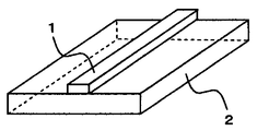
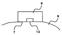
本発明において、配線基板とは電気配線回路基板を意味するものであり、それ故に表面配線、埋め込み配線とはすべて電気配線の態様を意味することとなり、さらには電気部品には電球、真空管、コンセント、コネクタ、トランス、リレー、インダクションコイル、安定化電源、乾電池などの一般的な電気部品があり、電子部品にはダイオード、コンデンサ、トランジスタ、発光ダイオード、集積回路、コイル、マイクロマシン、マイクロスイッチ、太陽電池などの一般的な電子部品がある。尚、図1は従来の配線基板における表面配線要部を示す概略透視図であるが、ここでは配線基板2の表面に表面配線1が配置されている構造のものを示しており、配線基板2の基材には一般に樹脂やセラミックス、ガラス等が使用される。さらに、図2は従来の配線基板における表面配線及び埋め込み配線要部を示す概略透視図である。ここでは、上層配線基板4の表面に表面配線1が配置され、下層配線基板5の表面に埋め込み配線3が配置されている構造のものを示しているが、この埋め込み配線3は上層配線基板4の内部に埋め込み配置されているというものである。この図2のように、表面配線及び埋め込み配線を有する従来の配線基板を製造する場合、初めに下層配線基板5の表面に埋め込み配線3を配置した後、上層配線基板4を埋め込み配線3を覆うように設け、その後に上層配線基板4の表面に表面配線1を設けることとなる。この従来の製造工程では、多層配線基板を製造する際、各層の製作及びその配線工程を繰り返すことが要求され、このことがコスト高の要因である。 In the present invention, the wiring board means an electric wiring circuit board. Therefore, the surface wiring and the embedded wiring all mean the form of the electric wiring. Furthermore, the electric parts include a light bulb, a vacuum tube, and an outlet. There are general electrical parts such as connectors, transformers, relays, induction coils, stabilized power supplies, dry batteries, etc., and electronic parts include diodes, capacitors, transistors, light emitting diodes, integrated circuits, coils, micromachines, microswitches, solar cells There are general electronic parts. FIG. 1 is a schematic perspective view showing a main part of a surface wiring in a conventional wiring board. Here, a structure in which the
本発明において、多糖質配線基板の原料である多糖質には、生物由来の安全かつ低コストの材料にて市販品の入手が容易であり、また多糖質水溶物の乾燥により固形化が容易かつ配線基板として使用する際の絶縁性及び強度を保持し得るという理由から、プルラン、カルボキシメチルセルロース、デンプン、ヒアルロン酸、から選択される1の多糖質であることが好適である。また、他の多糖質としては、上述の理由に加えて生体に親和性のある新規な成形素材であるという理由から、セルロース、グリコーゲン、キチン、ヘパリン、カラギーナン、アガロース、ペクチン、キシログルカンから選択される1の多糖質を使用することが好適である。また、本発明の多糖質配線基板の製造方法について、前記表面配線を有する構造の多糖質配線基板の製造においては、疎水性を有するモールド内に10重量%〜70重量%の多糖質水溶物を充填した後、前記モールドを湿度10%以下の乾燥大気中に静置することにより、又は前記モールドを50℃〜90℃に加熱することにより、前記モールド内に充填された前記多糖質水溶物を乾燥固形化して成形し、前記成形物の表面に電気部品及び/又は電子部品に結線可能な配線を設けるという製造方法が好適であり、また、前記埋め込み配線を有する構造の多糖質配線基板の製造においては、電気部品及び/又は電子部品に結線可能な配線を、疎水性を有するモールド内に配置し、前記モールド内に10重量%〜70重量%の多糖質水溶物を充填した後、前記モールドを湿度10%以下の乾燥大気中に静置することにより、又は前記モールドを50℃〜90℃に加熱することにより、前記モールド内に充填された前記多糖質水溶物を乾燥固形化して成形するという製造方法が好適である。次に、本発明の表面配線及び埋め込み配線を有する多糖質配線基板の製造方法においては、電気部品及び/又は電子部品に結線可能な配線を、疎水性を有するモールド内に配置し、前記モールド内に10重量%〜70重量%の多糖質水溶物を充填した後、前記モールドを湿度10%以下の乾燥大気中に静置することにより、又は前記モールドを50℃〜90℃に加熱することにより、前記モールド内に充填された前記多糖質水溶物を乾燥固形化して成形し、さらに前記成形物の表面に電気部品及び/又は電子部品に結線可能な配線を設けるという製造方法が好適である。すなわち、本発明において多糖質水溶物の濃度は10重量%〜70重量%が好適であるが、10重量%より小さい場合には多糖質水溶物の乾燥固形化に非常に多大な時間がかかり過ぎて製造に不適であるいう理由から、70重量%より大きい場合では多糖質水溶物の粘度が高過ぎてモールド成形が極めて困難になるという理由から好ましくない。また、本発明において乾燥大気の湿度は10%以下が好適であるが、10%より大きい場合には多糖質水溶物の乾燥に要する時間がかかり過ぎて製造に不適であるという理由から好ましくない。さらに、本発明において加熱温度は50℃〜90℃が好適であるが、50℃より小さい場合には多糖質水溶物の加熱温度が低過ぎて乾燥に多くの時間を要し生産効率が悪くなるという理由から、90℃より大きい場合では多糖質水溶物の加熱温度が高過ぎて多糖質の表面の乾燥速度と内部の乾燥速度に大きな差が発生し、乾燥後の多糖質に歪が発生し易くなるという理由から好ましくない。また、本発明において使用するモールドは疎水性であることが好適であるが、その理由は多糖質水溶物の乾燥成形後にモールド内壁からの成形物の離形がとても容易になるからであり、モールドの材質としては例えばステンレス、鉄、チタン、シリコンなどが好適に使用され、また加熱のない乾燥大気中での乾燥の場合には例えば樹脂などが好適に使用され、さらにその形状や分割に関る構造は特には限定されない。また、前記モールド内の前記多糖質水溶物を乾燥固形化する際の前記放置の時間並びに前記加熱の時間については、配線基板として使用に適した程度の強度があれば良く、特には限定されない。また、さらに前記成形物の表面に電気部品及び/又は電子部品に結線可能な配線を設ける方法であるが、単に配線を前記表面上に配置する方法、印刷技術を基にしたプリント配線による方法、真空蒸着法によりステンシルマスクを通してアルミ電気配線を前記表面上に設ける方法など種々にあるが、特に限定されるものではない。
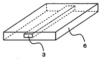
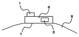
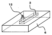
尚、図3は本発明の多糖質配線基板における表面配線要部を示す概略透視図であるが、ここでは多糖質配線基板6の表面に表面配線1が配置されている構造のものを示しており、図4は本発明の多糖質配線基板における埋め込み配線要部を示す概略透視図であるが、この図では多糖質配線基板6の内部に埋め込み配線3が配置されている構造のものを示している。また、図5は本発明の多糖質配線基板における表面配線及び埋め込み配線要部を示す概略透視図であるが、ここでは多糖質配線基板6の表面に表面配線1が配置され、かつ多糖質配線基板6の内部に埋め込み配線3が配置されている構造のものを示しており、従来の前記配線基板を示す図2と比べて多層(二層)構造でなく単層(一層)構造であることに留意すべきである。この単層構造化により、従来の前記配線基板に比して、製造時の低コスト化が成されることとなる。さらに、図6は本発明の多糖質配線基板を皮膚装着した場合の表面配線及び埋め込み配線要部の概略断面図であるが、ここでは多糖質配線基板6は皮膚8の表面に対して粘着面7を介して皮膚装着されているものである。この粘着面7は、多糖質配線基板6における皮膚との装着面を装着前に水で濡らすことにより湿潤面とすることで得られるものであり、前記の水で濡らす方法は刷毛、霧吹き器等を使用しても良く、特には限定されない。ちなみに、前記の粘着面7は多糖質を水で湿潤することにより、水溶性である多糖質が溶融して粘着性を有することに起因するものであり、本発明の種々の多糖質配線基板のいずれにおいても同様である。In the present invention, it is easy to obtain a commercially available polysaccharide as a raw material for a polysaccharide wiring board using a biologically safe and low-cost material, and it is easy to solidify by drying a polysaccharide aqueous solution. It is preferable that the polysaccharide is one polysaccharide selected from pullulan, carboxymethylcellulose, starch, and hyaluronic acid because it can retain insulation and strength when used as a wiring board. In addition to the above reasons, other polysaccharides are selected from cellulose, glycogen, chitin, heparin, carrageenan, agarose, pectin, and xyloglucan because they are novel molding materials that have an affinity for the living body. It is preferable to use one polysaccharide. Further, regarding the method for producing a polysaccharide wiring board of the present invention, in the production of the polysaccharide wiring board having the structure having the surface wiring, 10% by weight to 70% by weight of the polysaccharide aqueous solution is contained in a hydrophobic mold. After the filling, the polysaccharide aqueous solution filled in the mold is left by leaving the mold in a dry atmosphere with a humidity of 10% or less, or by heating the mold to 50 ° C. to 90 ° C. A manufacturing method of forming by drying and solidifying and providing a wiring that can be connected to an electrical component and / or an electronic component on the surface of the molded product is preferable, and manufacturing a polysaccharide wiring board having a structure having the embedded wiring , Wiring that can be connected to electrical components and / or electronic components is placed in a hydrophobic mold, and 10% to 70% by weight of a polysaccharide aqueous solution is filled in the mold. Then, the polysaccharide aqueous solution filled in the mold is dried by allowing the mold to stand in a dry atmosphere having a humidity of 10% or less, or by heating the mold to 50 ° C. to 90 ° C. A production method of solidifying and molding is preferred. Next, in the manufacturing method of the polysaccharide wiring board having the surface wiring and the embedded wiring according to the present invention, the wiring that can be connected to the electrical component and / or the electronic component is disposed in the hydrophobic mold, After filling 10% to 70% by weight polysaccharide aqueous solution, the mold is left in a dry atmosphere with a humidity of 10% or less, or the mold is heated to 50 ° C. to 90 ° C. A manufacturing method is preferable in which the polysaccharide aqueous solution filled in the mold is dried and solidified and molded, and an electric component and / or wiring that can be connected to the electronic component is provided on the surface of the molded product. That is, in the present invention, the concentration of the polysaccharide water solution is preferably 10% by weight to 70% by weight, but if it is less than 10% by weight, it takes too much time to dry and solidify the polysaccharide water solution. If it is more than 70% by weight, it is not preferable because the viscosity of the polysaccharide aqueous solution is too high and molding becomes extremely difficult. In the present invention, the humidity of the dry atmosphere is preferably 10% or less. However, if it is more than 10%, it takes too much time to dry the polysaccharide water solution, which is not suitable for production. Furthermore, in the present invention, the heating temperature is preferably 50 ° C. to 90 ° C., but if it is less than 50 ° C., the heating temperature of the polysaccharide aqueous solution is too low, and it takes a long time to dry, resulting in poor production efficiency. For this reason, when the temperature is higher than 90 ° C., the heating temperature of the polysaccharide aqueous solution is too high, resulting in a large difference between the surface drying speed of the polysaccharide and the internal drying speed, and distortion of the polysaccharide after drying. It is not preferable because it becomes easy. In addition, the mold used in the present invention is preferably hydrophobic, because it is very easy to release the molded product from the inner wall of the mold after dry molding of the polysaccharide aqueous solution. For example, stainless steel, iron, titanium, silicon and the like are preferably used as the material, and in the case of drying in a dry atmosphere without heating, for example, a resin is preferably used, and further, the shape and division are related. The structure is not particularly limited. Further, the standing time and the heating time in drying and solidifying the polysaccharide aqueous solution in the mold are not particularly limited as long as the strength is suitable for use as a wiring board. Further, it is a method of providing a wiring that can be connected to an electrical component and / or an electronic component on the surface of the molding, but a method of simply arranging the wiring on the surface, a method of printed wiring based on a printing technique, There are various methods such as a method of providing aluminum electrical wiring on the surface through a stencil mask by a vacuum deposition method, but it is not particularly limited.
FIG. 3 is a schematic perspective view showing the main part of the surface wiring in the polysaccharide wiring board of the present invention. Here, the structure in which the
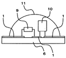
本発明において、多糖質配線基板の応用例として、図7には本発明におけるダイオード及びコンデンサを搭載した多糖質配線基板の配線要部を示す概略透視図を図示し、また図8には本発明におけるダイオード及びコンデンサを搭載した多糖質配線基板の配線要部の概略断面図を図示するが、ここでは多糖質配線基板6の表面において、表面配線1、並びにそれと結線したダイオード9及びコンデンサ10が配置されている構造のものが示されている。さらに図9には本発明における多糖質からなる絶縁体により封入された多糖質配線基板の配線要部の概略断面図を図示するが、ここでは図8で示した多糖質配線基板について、そこに配置された表面配線1、並びにそれと結線したダイオード9及びコンデンサ10が多糖質からなる絶縁体11によって封入されている構造のものが示されており、前記の表面配線1、並びにそれと結線したダイオード9及びコンデンサ10は多糖質からなる絶縁体11により保護され、配線回路基板としても安定に作動することとなる。ここで、多糖質からなる絶縁体11には、生物由来の安全かつ低コストの材料にて市販品の入手が容易であり、また多糖質水溶物の乾燥により固形化が容易かつ配線基板として使用する際の絶縁性及び強度を保持し得るという理由から、プルラン又はヒアルロン酸が好適に使用される。 In the present invention, as an application example of the polysaccharide wiring board, FIG. 7 shows a schematic perspective view showing a main part of the polysaccharide wiring board on which the diode and the capacitor according to the present invention are mounted, and FIG. 8 shows the present invention. FIG. 1 is a schematic cross-sectional view of a main part of a polysaccharide wiring board on which a diode and a capacitor are mounted. In FIG. 1, a
本発明において、皮膚装着可能な表面電極を有する多糖質配線基板には、多糖質からなる配線基板において、前記基板内部に配置された埋め込み配線の末端部が前記基板の表面に露呈された表面電極を有する構造であり、かつ前記配線が電気部品及び/又は電子部品に結線可能な配線であり、さらに前記表面電極が露呈された側の基板表面を湿潤させることにより前記基板が皮膚に粘着して前記表面電極が皮膚表面に接触するものが好適に使用される。尚、図10は本発明における表面電極を有する多糖質配線基板の配線要部を示す概略透視図であり、また図11は本発明の表面電極を有する多糖質配線基板を皮膚装着した場合の配線要部の概略断面図である。これらの図10及び図11では、多糖質配線基板6の内部に配置された埋め込み配線3の末端部が前記基板6の表面に露呈されて表面電極12となっている構造のものを示しており、また多糖質配線基板6は皮膚8の表面に対して粘着面7を介して皮膚装着され、表面電極12は皮膚8の表面と接触しているものである。この粘着面7は、多糖質配線基板6における皮膚との装着面を装着前に水で濡らすことにより湿潤面とすることで得られるものであり、前記の水で濡らす方法又は湿潤させる方法は刷毛、霧吹き器等を使用しても良く、特には限定されない。尚、前記の表面電極12の形状は皮膚表面と接触し易い形状であれば良く、特に限定されるものではなく、またその表面電極の材質は主に金属であるが、電極として作用するものであれば例えばアルミ、チタン、鉄、ステンレス、金、白金、銀などが好適に使用され、特に限定されない。 In the present invention, a polysaccharide wiring board having a skin-mountable surface electrode includes a polysaccharide-based wiring board, and a surface electrode in which a terminal portion of an embedded wiring disposed inside the board is exposed on the surface of the board And the wiring is a wiring that can be connected to an electrical component and / or an electronic component, and further, the substrate adheres to the skin by wetting the substrate surface on the side where the surface electrode is exposed. The surface electrode is preferably used in contact with the skin surface. FIG. 10 is a schematic perspective view showing a wiring main part of the polysaccharide wiring board having the surface electrode in the present invention, and FIG. 11 is a wiring when the polysaccharide wiring board having the surface electrode of the present invention is attached to the skin. It is a schematic sectional drawing of the principal part. 10 and 11 show a structure in which the end portion of the embedded
本発明において、皮膚装着可能な微細針電極を有する多糖質配線基板においては、多糖質からなる配線基板において、前記基板内部に配置された埋め込み配線の末端部と結線され、前記基板の表面に露呈された微細針電極を有する構造であり、かつ前記配線が電気部品及び/又は電子部品に結線可能な配線であり、さらに前記微細針電極が露呈された側の基板表面を湿潤させることにより前記基板が皮膚に粘着して前記微細針電極が皮膚表面に挿入するものが好適である。尚、図12は本発明における微細針電極を有する多糖質配線基板の配線要部を示す概略透視図であり、また図13は本発明の微細針電極を有する多糖質配線基板を皮膚装着した場合の配線要部の概略断面図である。これらの図12及び図13では、多糖質配線基板6の内部に配置された埋め込み配線3の末端部が前記基板6の表面に露呈されて微細針電極13となっている構造のものを示しており、また多糖質配線基板6は皮膚8の表面に対して粘着面7を介して皮膚装着され、微細針電極13は皮膚8の表面に挿入しているものである。この粘着面7は、多糖質配線基板6における皮膚との装着面を装着前に水で濡らすことにより湿潤面とすることで得られるものであり、前記の水で濡らす方法又は湿潤させる方法は刷毛、霧吹き器等を使用しても良く、特には限定されない。尚、前記の微細針電極13の形状は皮膚表面に挿入し易い形状であれば良く、特に限定されるものではなく、またその微細針電極の材質は主に金属であるが、電極として作用するものであれば例えばアルミ、チタン、鉄、ステンレス、金、白金、銀などが好適に使用され、特に限定されない。 In the present invention, in the polysaccharide wiring board having fine needle electrodes that can be attached to the skin, the polysaccharide wiring board is connected to the end of the embedded wiring disposed inside the substrate and exposed to the surface of the board. And the wiring is a wiring that can be connected to an electrical component and / or an electronic component, and further, the substrate surface on the side where the fine needle electrode is exposed is wetted to form the substrate. It is preferable that the electrode adheres to the skin and the fine needle electrode is inserted into the skin surface. FIG. 12 is a schematic perspective view showing a wiring main part of the polysaccharide wiring board having fine needle electrodes in the present invention, and FIG. 13 is a case where the polysaccharide wiring board having fine needle electrodes of the present invention is attached to the skin. It is a schematic sectional drawing of the wiring principal part. 12 and 13 show a structure in which the terminal portion of the embedded
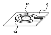
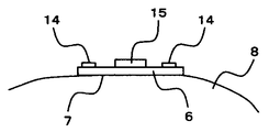
本発明において、皮膚装着可能なスピーカを搭載する多糖質配線基板においては、多糖質からなる配線基板において、前記基板表面に配置された磁気コイル配線、及び前記磁気コイル配線内に配置された磁性体を有する構造であり、かつ前記磁気コイル配線が電気部品及び/又は電子部品に結線可能な配線であり、さらに前記磁性体が配置された基板表面と反対側の基板表面を湿潤させることにより前記基板が皮膚に粘着し、前記磁気コイル配線に通電して前記磁性体を振動させることによりスピーカとして皮膚内に音声信号を伝導するものが好適に使用され得る。尚、図14は本発明における皮膚装着可能なスピーカを搭載する多糖質配線基板の配線要部を示す概略図であり、また図15は本発明の皮膚装着可能なスピーカを搭載する多糖質配線基板を皮膚装着した場合の配線要部の概略断面図である。図14及び図15では、多糖質配線基板6の表面に磁気コイル配線14及び前記磁気コイル配線14内に配置された磁性体15を有する構造のものが示されており、また多糖質配線基板6は皮膚8の表面に対して粘着面7を介して皮膚装着され、前記磁気コイル配線14に通電して前記磁性体15を振動させることによりスピーカとして皮膚内に音声信号を伝導するものである。この粘着面7は、多糖質配線基板6における皮膚との装着面を装着前に水で濡らすことにより湿潤面とすることで得られるものであり、前記の水で濡らす方法は刷毛、霧吹き器等を使用しても良く、特には限定されない。尚、前記の磁気コイル配線14及び磁性体15の形状、並びに構造はスピーカとしての機能を好適に発揮するものであれば良く、特には限定されるものではない。また、前記の多糖質配線基板6は皮膚8の表面に対して粘着面7を介して皮膚装着する際、音声信号を効率よく皮膚及び骨に伝導するためには隙間なく皮膚装着されることが好ましい。 In the present invention, in the polysaccharide wiring board on which the skin-worn speaker is mounted, in the wiring board made of polysaccharide, the magnetic coil wiring disposed on the substrate surface, and the magnetic body disposed in the magnetic coil wiring The magnetic coil wiring is a wiring that can be connected to an electrical component and / or an electronic component, and the substrate surface on the side opposite to the substrate surface on which the magnetic body is disposed is moistened. That adheres to the skin and conducts an audio signal in the skin can be suitably used as a speaker by vibrating the magnetic material by energizing the magnetic coil wiring. FIG. 14 is a schematic diagram showing the main wiring part of the polysaccharide wiring board on which the skin-mountable speaker according to the present invention is mounted, and FIG. 15 shows the polysaccharide wiring board on which the skin-mountable speaker of the present invention is mounted. It is a schematic sectional drawing of the wiring main part at the time of mounting | wearing with skin. 14 and 15 show a structure having a
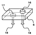
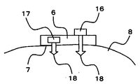
本発明において、皮膚装着可能な発光ダイオードを搭載する多糖質配線基板には、多糖質からなる配線基板において、前記基板表面に配置された表面配線及び/又は前記基板内部に配置された埋め込み配線と結線され、前記基板の表面に配置された発光ダイオード及び/又は前記基板内部に埋め込み配置された発光ダイオードを有する構造であり、かつ前記配線が電気部品及び/又は電子部品に結線可能な配線であり、さらに前記基板表面を湿潤させることにより前記基板が皮膚に粘着し、前記基板の表面に配置された発光ダイオード及び/又は前記基板内部に埋め込み配置された発光ダイオードにより皮膚表面を照光するものが好適に使用される。尚、図16は本発明における皮膚装着可能な発光ダイオードを搭載する多糖質配線基板の基板要部を示す概略透視図であり、図17は本発明の皮膚装着可能な発光ダイオードを搭載する多糖質配線基板を皮膚装着した場合の配線要部の概略断面図である。これらの図16及び図17では、多糖質配線基板6の基板表面に配置された発光ダイオード16及びその基板内部に埋め込み配置された発光ダイオード17を有する構造のものを示しており、また多糖質配線基板6は皮膚8の表面に対して粘着面7を介して皮膚装着され、前記の発光ダイオード16及び17からの光照射については、発光ダイオードからの照射光の進行方向を示す矢印18により図示されているように、皮膚8の表面を光照射し、さらには皮膚8の内部にまで光が届いているものである。また、この粘着面7は多糖質配線基板6における皮膚との装着面を装着前に水で濡らすことにより湿潤面とすることで得られるものであり、前記の水で濡らす方法は刷毛、霧吹き器等を使用しても良く、特に限定されない。尚、前記の発光ダイオード16及び17の形状、構造等は基板表面に効率的に配置され、効率よく光照射するものであれば良く、特に形状及び構造等は限定されるものではない。ちなみに、図16及び図17についてはともに図の煩雑化を避けるべく、前記の発光ダイオード16及び17の結線配線は省略してあることに留意すべきである。 In the present invention, the polysaccharide wiring board on which the skin-mountable light emitting diode is mounted includes a surface wiring arranged on the substrate surface and / or an embedded wiring arranged inside the board in the polysaccharide wiring board. A light-emitting diode that is connected and arranged on the surface of the substrate and / or a light-emitting diode that is embedded in the substrate, and the wiring is a wiring that can be connected to an electrical component and / or an electronic component. Further, it is preferable that the substrate adheres to the skin by moistening the substrate surface, and the surface of the skin is illuminated by the light-emitting diode disposed on the surface of the substrate and / or the light-emitting diode embedded in the substrate. Used for. FIG. 16 is a schematic perspective view showing the main part of the polysaccharide wiring board on which the skin-mounted light-emitting diode according to the present invention is mounted, and FIG. 17 is a polysaccharide on which the skin-mounted light-emitting diode of the present invention is mounted. It is a schematic sectional drawing of the principal part of wiring at the time of mounting a wiring board on skin. 16 and 17 show a structure having a
本発明について、以下に実施例をあげて具体的説明を行うが、本発明はこれらの実施例に何ら限定されるものではない。 The present invention will be specifically described below with reference to examples, but the present invention is not limited to these examples.
表面配線を有したプルラン配線基板の作製及びその絶縁性試験
疎水性を有するステンレス製モールド(内側凹部が縦長さ0.3cm、横長さ1cm、幅3cmの直方体形状であり、上面は開放されているキャスティングモールド)内に原料である60重量%のプルラン水溶物を充填した後、このモールドを60℃に加熱(約30分間)することによりモールド内に充填されたプルラン水溶物を乾燥固形化して成形を行い、図3に示した様な直方体形状のプルラン基板を作製した。次に、本プルラン基板の上面において、電気部品及び/又は電子部品に結線可能な電気配線を設けるべく、真空蒸着法により配線形状の隙間をもつステンシルマスクを通して1本のアルミ電気配線(厚さ0.005mm、幅0.1mm、長さ3cm)を図3に示した様に所定の位置に設け、プルラン配線基板を作製した。尚、前記モールド内からの本成形物の取り出しについては、前記モールド内で成形物が乾燥により若干縮小し、またモールド内側凹部壁は疎水性を有するので、成形物は前記モールドから自然に離形することとなり、さらに、本成形物は、配線基板として使用に適した程度の強度を保持しており、これらのことは以下の実施例においても同様であった。また、本実施例において本成形物は直方体形状をなすが、その構成要件である3辺を縦長さ、横長さ、幅と呼ぶこととし、従って本成形物の縦長さ及び横長さとは、図3において最手前にある長方形の縦長さ及び横長さを意味し、本成形物の幅とは前記長方形及びこれと向い合う長方形との距離を表す辺を意味することとなる。それ故に、本成形物の形状はそのままモールド内側凹部の形状と同様になるため、モールド内側凹部についても前記の縦長さ、横長さ、幅の3辺を用いて大きさを表すこととし、以下の実施例においても成形物の形状及びモールド内側凹部の形状を表す3辺について上述と同様に呼ぶとすることに留意する必要がある。次に、プルラン配線基板について絶縁性試験を行うべく、上述の製作方法において独立した2本のアルミ電気配線(厚さ0.005mm、幅0.1mm、長さ3cm)を設ける、とした以外は上述の製作方法と同様にして絶縁性試験用プルラン配線基板を作製し、前記2本の電気配線間の電気抵抗を測定したところ、抵抗が2MΩ以上の絶縁性を有することを確認した。Fabrication of pullulan wiring board having surface wiring and insulation test thereof Hydrophobic stainless steel mold (inner recess is in a rectangular parallelepiped shape with a longitudinal length of 0.3 cm, a lateral length of 1 cm, and a width of 3 cm, and the upper surface is open. Casting mold) is filled with 60% by weight pullulan aqueous solution, which is the raw material, and then heated to 60 ° C (about 30 minutes) to dry and solidify the pullulan aqueous solution filled in the mold. A rectangular parallelepiped pullulan substrate as shown in FIG. 3 was produced. Next, in order to provide an electrical wiring that can be connected to an electrical component and / or an electronic component on the upper surface of the pullulan substrate, one aluminum electrical wiring (thickness 0) is passed through a stencil mask having a wiring-shaped gap by vacuum deposition. .005 mm, width 0.1 mm, and
表面配線を有したカルボキシメチルセルロース配線基板の作製及びその絶縁性試験
実施例1において、原料に50重量%のカルボキシメチルセルロース水溶物を使用し、原料充填後のモールド内容物の乾燥固形化を湿度5%の乾燥大気中に静置(約60分間)することによる、とした以外は実施例1と同様にして、図3に示した様な直方体形状のカルボキシメチルセルロース基板を作製した。次に、カルボキシメチルセルロース配線基板について絶縁性試験を行うべく、上述の製作方法において独立した2本のアルミ電気配線(厚さ0.005mm、幅0.1mm、長さ3cm)を設ける、とした以外は上述の製作方法と同様にして絶縁性試験用カルボキシメチルセルロース配線基板を作製し、前記2本の電気配線間の電気抵抗を測定したところ、抵抗が2MΩ以上の絶縁性を有することを確認した。Production of carboxymethylcellulose wiring board having surface wiring and insulation test thereof In Example 1, 50% by weight carboxymethylcellulose aqueous solution was used as a raw material, and the mold content after filling the raw material was dried and solidified at a humidity of 5%. A rectangular parallelepiped carboxymethyl cellulose substrate as shown in FIG. 3 was produced in the same manner as in Example 1 except that the substrate was left in a dry atmosphere (about 60 minutes). Next, in order to conduct an insulation test on the carboxymethylcellulose wiring board, except that two independent aluminum electrical wirings (thickness 0.005 mm, width 0.1 mm,
埋め込み配線を有したヒアルロン酸配線基板の作製及びその絶縁性試験
電気部品及び/又は電子部品に結線可能な銅配線(厚さ0.05mm、幅0.3mm、長さ3cm)について、疎水性を有するステンレス製モールド(内側凹部が縦長さ0.3cm、横長さ1cm、幅3cmの直方体形状であり、上面は開放されているキャスティングモールド)内に図7で図示したように所定の空間配置を行った。次に、このモールド内に原料である50重量%のヒアルロン酸水溶物を充填した後、このモールドを50℃に加熱(約50分間)することによりモールド内に充填されたヒアルロン酸水溶物を乾燥固形化して成形を行い、図4に示した様な直方体形状のヒアルロン酸配線基板を作製した。次に、ヒアルロン酸配線基板について絶縁性試験を行うべく、上述の製作方法において独立した2本の銅電気配線(厚さ0.05mm、幅0.3mm、長さ3cm)を設ける、とした以外は上述の製作方法と同様にして絶縁性試験用ヒアルロン酸配線基板を作製し、前記2本の電気配線間の電気抵抗を測定したところ、抵抗が2MΩ以上の絶縁性を有することを確認した。Preparation of hyaluronic acid wiring board with embedded wiring and its insulation test Copper wiring (thickness 0.05mm, width 0.3mm, length 3cm) that can be connected to electrical and / or electronic components is hydrophobic. As shown in FIG. 7, a predetermined space arrangement is performed in a stainless steel mold (a casting mold in which an inner concave portion is a rectangular parallelepiped shape having a longitudinal length of 0.3 cm, a lateral length of 1 cm, a width of 3 cm, and an upper surface being opened). It was. Next, after filling the mold with 50% by weight hyaluronic acid aqueous solution as a raw material, the mold is heated to 50 ° C. (about 50 minutes) to dry the hyaluronic acid aqueous solution filled in the mold. Solidified and molded, a rectangular parallelepiped hyaluronic acid wiring board as shown in FIG. 4 was produced. Next, in order to conduct an insulation test on the hyaluronic acid wiring board, two independent copper electric wirings (thickness 0.05 mm, width 0.3 mm,
埋め込み配線を有したデンプン配線基板の作製及びその絶縁性試験
実施例3において、原料に40重量%のデンプン水溶物を使用し、原料充填後のモールド内容物の乾燥固形化を湿度5%の乾燥大気中に静置(約70分間)することによる、とした以外は実施例3と同様にして、図4に示した様な直方体形状のデンプン配線基板を作製した。次に、デンプン配線基板について絶縁性試験を行うべく、上述の製作方法において独立した2本の銅電気配線(厚さ0.05mm、幅0.3mm、長さ3cm)を設ける、とした以外は上述の製作方法と同様にして絶縁性試験用デンプン配線基板を作製し、前記2本の電気配線間の電気抵抗を測定したところ、抵抗が2MΩ以上の絶縁性を有することを確認した。Preparation of starch wiring board having embedded wiring and insulation test thereof In Example 3, 40% by weight of starch aqueous solution was used as a raw material, and drying and solidification of the mold contents after filling the raw material was performed at a humidity of 5%. A rectangular parallelepiped-shaped starch wiring board as shown in FIG. 4 was produced in the same manner as in Example 3 except that it was left in the atmosphere (about 70 minutes). Next, in order to conduct an insulation test on the starch wiring board, two independent copper electric wirings (thickness 0.05 mm, width 0.3 mm,
表面配線及び埋め込み配線を有したプルラン配線基板の作製及びその皮膚装着試験
始めに埋め込み配線を有した配線基板を作製するべく、電気部品及び/又は電子部品に結線可能な銅配線(厚さ0.05mm、幅0.3mm、長さ3cm)について、疎水性を有するステンレス製モールド(内側凹部が縦長さ1cm、横長さ2cm、幅3cmの直方体形状であり、上面は開放されているキャスティングモールド)内に図5で図示したように所定の空間配置を行った。次に、このモールド内に原料である60重量%のプルラン水溶物を充填した後、このモールドを60℃に加熱(約30分間)することによりモールド内に充填されたプルラン水溶物を乾燥固形化して成形を行い、図5に示した様な埋め込み配線を有した、直方体形状のプルラン配線基板を作製した。次に、本プルラン基板の上面において、電気部品及び/又は電子部品に結線可能な電気配線を設けるべく、真空蒸着法により配線形状の隙間をもつステンシルマスクを通して1本のアルミ電気配線(厚さ0.005mm、幅0.3mm、長さ3cm)を図5に示した様に所定の位置に設け、表面配線及び埋め込み配線を有したプルラン配線基板を作製した。次に、本プルラン配線基板において、表面配線の配置面の裏側面について刷毛を用いて水で湿潤させることにより、その裏側面を粘着面として皮膚装着試験を行ったところ、粘着面の接着作用により本プルラン配線基板は図6に示した様に皮膚に密着することを確認した。Preparation of pull-run wiring board having surface wiring and embedded wiring and skin mounting test First, copper wiring (thickness 0. 0) that can be connected to an electrical component and / or an electronic component in order to manufacture a wiring substrate having embedded wiring. 05mm, width 0.3mm, length 3cm) in a hydrophobic stainless steel mold (a casting mold in which the inner recess has a rectangular parallelepiped shape with a longitudinal length of 1cm, a lateral length of 2cm, a width of 3cm, and an open top surface) As shown in FIG. 5, a predetermined spatial arrangement was performed. Next, after filling the mold with 60% by weight pullulan aqueous solution as a raw material, the mold is heated to 60 ° C. (about 30 minutes) to dry and solidify the pullulan aqueous solution filled in the mold. A rectangular parallelepiped pullulan wiring board having embedded wiring as shown in FIG. 5 was produced. Next, in order to provide an electrical wiring that can be connected to an electrical component and / or an electronic component on the upper surface of the pullulan substrate, one aluminum electrical wiring (thickness 0) is passed through a stencil mask having a wiring-shaped gap by vacuum deposition. .005 mm, width 0.3 mm, and
コンデンサ及びダイオードを有したプルラン配線基板の作製及びその機能確認試験
疎水性を有するステンレス製モールド(内側凹部が縦長さ1cm、横長さ2cm、幅3cmの直方体形状であり、上面は開放されているキャスティングモールド)内に原料である40重量%のプルラン水溶物を充填した後、このモールドを70℃に加熱(約30分間)することによりモールド内に充填されたプルラン水溶物を乾燥固形化して成形を行い、図7及び図8に示した様な直方体形状のプルラン基板を作製した。次に、本プルラン基板の上面において、電気部品及び/又は電子部品に結線可能な電気配線を設けるべく、真空蒸着法によりステンシルマスクを通してアルミ電気配線(厚さ0.005mm、幅0.3mm、長さ3cm)を図7及び図8に示した様に所定の位置に設けた後、1μFのコンデンサ及び小型ダイオードを所定の位置に結線させ、コンデンサ及びダイオードを有したプルラン配線基板を作製した。次に、前記の配線に電気を通したところ、前記のコンデンサ及びダイオードが正常に機能を発揮することを確認した。Fabrication of pullulan wiring board with capacitors and diodes and their function confirmation test Hydrophobic stainless steel mold (inner recess is 1 cm in length, 2 cm in width, 3 cm in width, and the top surface is open casting After filling 40% by weight pullulan aqueous solution as a raw material in the mold), this mold is heated to 70 ° C. (about 30 minutes) to dry and solidify the pullulan aqueous solution filled in the mold. A rectangular parallelepiped pullulan substrate as shown in FIGS. 7 and 8 was produced. Next, on the upper surface of the pullulan substrate, an aluminum electrical wiring (thickness 0.005 mm, width 0.3 mm, long length) is formed through a stencil mask by vacuum deposition in order to provide electrical wiring that can be connected to electrical components and / or electronic components. 7 cm) was provided at a predetermined position as shown in FIGS. 7 and 8, and a 1 μF capacitor and a small diode were connected to the predetermined position to produce a pullulan wiring board having the capacitor and the diode. Next, when electricity was passed through the wiring, it was confirmed that the capacitor and the diode normally functioned.
プルランからなる絶縁体により封入された、コンデンサ及びダイオードを有したプルラン配線基板の作製
実施例6で作製したコンデンサ及びダイオードを有したプルラン配線基板について、その配線基板表面を図9に示した様にプルランからなる絶縁体により封入するべく、流動性の低い50重量%のプルラン水溶物を用いて前記配線基板の表面をディップ法により封入し、このプルラン水溶物の乾燥固形化を湿度5%の乾燥大気中に静置(約60分間)することにより行い、図9に示した様なプルランからなる絶縁体により封入された、コンデンサ及びダイオードを有したプルラン配線基板を作製した。尚、本プルラン配線基板については、プルランからなる絶縁体により封入された部分も使用に適した程度の保護強度を保持した。Fabrication of Pullulan Wiring Board Having Capacitor and Diode Encapsulated by an Insulator Made of Pullulan For the pullulan wiring board having the capacitor and diode fabricated in Example 6, the wiring board surface is as shown in FIG. In order to enclose with an insulator made of pullulan, the surface of the wiring board is encapsulated by dipping method using 50% by weight pullulan aqueous solution having low fluidity, and the solidification of the pullulan aqueous solution is dried at a humidity of 5%. A pullulan wiring substrate having a capacitor and a diode encapsulated by an insulator made of pullulan as shown in FIG. 9 was produced by standing in the atmosphere (about 60 minutes). In addition, about this pull run wiring board, the part enclosed with the insulator which consists of pull runs also kept the protection strength of the grade suitable for use.
表面電極を有したプルラン配線基板の作製及びその皮膚装着試験
電気部品及び/又は電子部品に結線可能なチタン配線(厚さ0.5mm、幅3mm、長さ1cm)について、疎水性を有するステンレス製モールド(内側凹部が縦長さ0.3cm、横長さ1cm、幅1.5cmの直方体形状であり、上面は開放されているキャスティングモールド)内に図10で図示したように所定の空間配置を行った。この時、埋め込み配線(チタン線)は成形物であるプルラン配線基板の表面に適宜露呈するように空間配置することが肝要である。次に、このモールド内に原料である60重量%のプルラン水溶物を充填した後、このモールドを60℃に加熱(約30分間)することによりモールド内に充填されたプルラン水溶物を乾燥固形化して成形を行い、図10に示した様な表面電極を有した直方体形状のプルラン配線基板を作製した。次に、本プルラン配線基板において、前記表面電極が露呈された側の基板表面について(表面電極の表面を除く)刷毛を用いて水で湿潤させることにより、その湿潤面を粘着面として皮膚装着試験を行ったところ、粘着面の接着作用により本プルラン配線基板及び表面電極は図11に示した様に皮膚に密着することを確認した。Fabrication of pullulan wiring board with surface electrode and skin mounting test Titanium wiring (thickness 0.5 mm,
微細針電極を有したヒアルロン酸配線基板の作製及びその皮膚装着試験
電気部品及び/又は電子部品に結線可能なチタン配線(厚さ0.5mm、幅3mm、長さ1cm)及びその配線に結線した微細針(底面が縦長さ及び横長さともに1mm、高さ2mmの四角錐形状のチタン製微細針)について、疎水性を有するステンレス製モールド(内側凹部が縦長さ0.3cm、横長さ1cm、厚さ1.5cmの直方体形状であり、上面は開放されているキャスティングモールド)内に図12で図示したように所定の空間配置を行った。この時、微細針は成形物であるプルラン配線基板の表面に適宜露呈するように空間配置することが肝要である。次に、このモールド内に原料である50重量%のヒアルロン酸水溶物を充填した後、このモールドを湿度5%の乾燥大気中に静置(約60分間)することによりモールド内に充填されたヒアルロン酸水溶物を乾燥固形化して成形を行い、図12に示した様な微細針電極を有した直方体形状のプルラン配線基板を作製した。次に、本ヒアルロン酸配線基板において、前記微細針電極が露呈された側の基板表面について(微細針電極の表面を除く)刷毛を用いて水で湿潤させることにより、その湿潤面を粘着面として皮膚装着試験を行ったところ、図13に示した様に、粘着面の接着作用により本ヒアルロン酸配線基板は皮膚に密着し、さらに微細針電極は皮膚表面内に挿入されることを確認した。Fabrication of hyaluronic acid wiring board with fine needle electrode and skin mounting test Titanium wiring (thickness 0.5 mm,
スピーカを搭載したプルラン配線基板の作製及びその皮膚装着試験
疎水性を有するステンレス製モールド(内側凹部が縦長さ0.3mm、横長さ1cm、幅1cmの直方体形状であり、上面は開放されているキャスティングモールド)内に原料である60重量%のプルラン水溶物を充填した後、このモールドを60℃に加熱(約30分間)することによりモールド内に充填されたプルラン水溶物を乾燥固形化して成形を行い、図14に示した様な直方体形状のプルラン基板を作製した。その後に、本プルラン基板の上面において、電気部品及び/又は電子部品に結線可能な電気配線を設けるべく、真空蒸着法により配線形状の隙間をもつステンシルマスクを通して円形コイル状のアルミ電気配線(円形部の直径0.5cm、直線部の長さ0.25cm、幅0.5mm、厚さ0.005mm)を図14に示した様に所定の位置に設け、プルラン配線基板を作製した。また、本プルラン基板の上面において、前記の磁気コイル配線内に磁性体(直径0.2cm、厚さ0.1cm)を図14に示した様に所定の位置に配置することにより、スピーカを搭載したプルラン配線基板を作製した。次に、本プルラン配線基板において、前記磁性体が配置された基板表面と反対側の基板表面について刷毛を用いて水で湿潤させることにより、その湿潤面を粘着面として手の甲の部位に対して皮膚装着試験を行ったところ、粘着面の接着作用により本プルラン配線基板及び表面電極は図15に示した様に皮膚に密着することを確認した。さらに、その密着状態において、前記磁気コイル配線に音声信号となる電気を通したところ、前記磁性体が振動することにより音声信号が手の甲の部位における皮膚内に伝導されることを確認した。Fabrication of pullulan wiring board with speaker and skin mounting test Hydrophobic stainless steel mold (inner recess is 0.3mm in length, 1cm in width, 1cm in width, cuboid shape, upper surface is open casting After filling 60% by weight pullulan aqueous solution as a raw material in the mold), this mold is heated to 60 ° C. (about 30 minutes) to dry and solidify the pullulan aqueous solution filled in the mold. Then, a rectangular parallelepiped pullulan substrate as shown in FIG. 14 was produced. Thereafter, in order to provide electrical wiring that can be connected to electrical components and / or electronic components on the upper surface of the pull-run substrate, a circular coil-shaped aluminum electrical wiring (circular portion) is formed through a stencil mask having a wiring-shaped gap by vacuum deposition. Were provided at predetermined positions as shown in FIG. 14 to produce a pullulan wiring board. Further, on the upper surface of the pullulan substrate, a magnetic body (diameter 0.2 cm, thickness 0.1 cm) is disposed in a predetermined position in the magnetic coil wiring as shown in FIG. A pullulan wiring board was prepared. Next, in this pullulan wiring board, the surface of the substrate opposite to the surface of the substrate on which the magnetic material is disposed is wetted with water using a brush, and the wet surface is used as an adhesive surface against the back of the hand. When a mounting test was performed, it was confirmed that the pullulan wiring board and the surface electrode were in close contact with the skin as shown in FIG. Furthermore, when electricity as an audio signal was passed through the magnetic coil wiring in the close contact state, it was confirmed that the audio signal was conducted into the skin on the back of the hand when the magnetic body vibrated.
発光ダイオードを搭載したプルラン配線基板の作製及びその皮膚装着試験
発光ダイオード、並びにそれと結線する銅配線(厚さ0.5mm、幅1mm、長さ1cm)について、疎水性を有するステンレス製モールド(内側凹部が縦長さ0.5cm、横長さ1cm、幅1cmの直方体形状であり、上面は開放されているキャスティングモールド)内に図16及び図17で図示したように所定の空間配置を行った。但し、図16及び図17では図の煩雑化を避けるべく、発光ダイオードに結線する配線はすべて省略してある。次に、このモールド内に原料である50重量%のプルラン水溶物を充填した後、このモールドを60℃に加熱(約30分間)することによりモールド内に充填されたプルラン水溶物を乾燥固形化して成形を行い、図16に示した様な埋め込み配置された発光ダイオードを有した直方体形状のプルラン配線基板を作製した。次に、その配線基板上面において、電気部品及び/又は電子部品に結線可能な電気配線を設けるべく、真空蒸着法により配線形状の隙間をもつステンシルマスクを通してアルミ電気配線(厚さ0.005mm、幅0.1mm、長さ1cm)及びそれと結線する発光ダイオードを所定の位置に設け、図16に示した様な埋め込み配置及び表面配置された発光ダイオードを有した直方体形状のプルラン配線基板を作製した。次に、本プルラン配線基板において、前記基板下面について刷毛を用いて水で湿潤させることにより、その湿潤面を粘着面として皮膚装着試験を行ったところ、粘着面の接着作用により本プルラン配線基板は図17に示した様に皮膚に密着することを確認した。さらに、その密着状態において、前記の銅及びアルミの結線配線に電気を通したところ、埋め込み配置及び表面配置された発光ダイオードより各々光照射して皮膚表面を照光することを確認した。Fabrication of pullulan wiring board mounted with light emitting diode and skin mounting test thereof Light emitting diode and copper wiring (thickness 0.5 mm,
本発明の多糖質配線基板及びその製造方法は、前述の通り様々な特徴的効果を有するが、これらの効果を活かして配線基板技術分野、電極の皮膚装着技術分野、骨伝導スピーカの技術分野、発光ダイオードの応用技術分野等において実用的に利用され得る。また、本発明の多糖質配線基板及びその製造方法は量産実施が可能なものであり、産業上利用できるものである。 The polysaccharide wiring board of the present invention and the method for producing the same have various characteristic effects as described above. Utilizing these effects, the wiring board technical field, the electrode skin mounting technical field, the bone conduction speaker technical field, It can be practically used in the field of application technology of light emitting diodes. Moreover, the polysaccharide wiring board and the manufacturing method thereof of the present invention can be mass-produced and can be used industrially.
1 表面配線
2 配線基板
3 埋め込み配線
4 上層配線基板
5 下層配線基板
6 多糖質配線基板
7 粘着面
8 皮膚
9 ダイオード
10 コンデンサ
11 多糖質からなる絶縁体
12 表面電極
13 微細針電極
14 磁気コイル配線
15 磁性体
16 基板表面に配置された発光ダイオード
17 基板内部に埋め込み配置された発光ダイオード
18 発光ダイオードからの照射光の進行方向を示す矢印DESCRIPTION OF
Claims (12)
Priority Applications (1)
| Application Number | Priority Date | Filing Date | Title |
|---|---|---|---|
| JP2008335999A JP2010141278A (en) | 2008-12-10 | 2008-12-10 | Polysaccharide wiring board and method of manufacturing the same |
Applications Claiming Priority (1)
| Application Number | Priority Date | Filing Date | Title |
|---|---|---|---|
| JP2008335999A JP2010141278A (en) | 2008-12-10 | 2008-12-10 | Polysaccharide wiring board and method of manufacturing the same |
Publications (1)
| Publication Number | Publication Date |
|---|---|
| JP2010141278A true JP2010141278A (en) | 2010-06-24 |
Family
ID=42351113
Family Applications (1)
| Application Number | Title | Priority Date | Filing Date |
|---|---|---|---|
| JP2008335999A Pending JP2010141278A (en) | 2008-12-10 | 2008-12-10 | Polysaccharide wiring board and method of manufacturing the same |
Country Status (1)
| Country | Link |
|---|---|
| JP (1) | JP2010141278A (en) |
Cited By (2)
| Publication number | Priority date | Publication date | Assignee | Title |
|---|---|---|---|---|
| CN108901131A (en) * | 2018-07-23 | 2018-11-27 | 清华大学 | The production method of printed circuit board and printed circuit board |
| CN111642067A (en) * | 2019-03-01 | 2020-09-08 | 北京梦之墨科技有限公司 | Circuit substrate, flexible thin film circuit and manufacturing method thereof |
Citations (5)
| Publication number | Priority date | Publication date | Assignee | Title |
|---|---|---|---|---|
| JPH0745575B2 (en) * | 1992-10-14 | 1995-05-17 | 工業技術院長 | Method for producing water-insoluble polysaccharide polymer film |
| JP2001352176A (en) * | 2000-06-05 | 2001-12-21 | Fuji Xerox Co Ltd | Multilayer printed wiring board and manufacturing method of multilayer printed wiring board |
| WO2008010573A1 (en) * | 2006-07-21 | 2008-01-24 | Elegaphy, Inc. | Microimplement, process for manufacturing the same, and method of assembling sugar material part |
| JP2008279237A (en) * | 2007-05-14 | 2008-11-20 | Yoshiichi Tobinaga | Cusp type skin surface inserting micro-needle |
| JP2008284318A (en) * | 2007-05-15 | 2008-11-27 | Kosumedei Seiyaku Kk | Microneedle for dosing, including living body origin matter |
-
2008
- 2008-12-10 JP JP2008335999A patent/JP2010141278A/en active Pending
Patent Citations (5)
| Publication number | Priority date | Publication date | Assignee | Title |
|---|---|---|---|---|
| JPH0745575B2 (en) * | 1992-10-14 | 1995-05-17 | 工業技術院長 | Method for producing water-insoluble polysaccharide polymer film |
| JP2001352176A (en) * | 2000-06-05 | 2001-12-21 | Fuji Xerox Co Ltd | Multilayer printed wiring board and manufacturing method of multilayer printed wiring board |
| WO2008010573A1 (en) * | 2006-07-21 | 2008-01-24 | Elegaphy, Inc. | Microimplement, process for manufacturing the same, and method of assembling sugar material part |
| JP2008279237A (en) * | 2007-05-14 | 2008-11-20 | Yoshiichi Tobinaga | Cusp type skin surface inserting micro-needle |
| JP2008284318A (en) * | 2007-05-15 | 2008-11-27 | Kosumedei Seiyaku Kk | Microneedle for dosing, including living body origin matter |
Cited By (3)
| Publication number | Priority date | Publication date | Assignee | Title |
|---|---|---|---|---|
| CN108901131A (en) * | 2018-07-23 | 2018-11-27 | 清华大学 | The production method of printed circuit board and printed circuit board |
| CN111642067A (en) * | 2019-03-01 | 2020-09-08 | 北京梦之墨科技有限公司 | Circuit substrate, flexible thin film circuit and manufacturing method thereof |
| CN111642067B (en) * | 2019-03-01 | 2025-04-18 | 北京梦之墨科技有限公司 | A circuit substrate, a flexible film circuit and a manufacturing method thereof |
Similar Documents
| Publication | Publication Date | Title |
|---|---|---|
| Yin et al. | Highly stretchable, ultrasensitive, and wearable strain sensors based on facilely prepared reduced graphene oxide woven fabrics in an ethanol flame | |
| CN105895303B (en) | Electrode structure, electronic component using the same, and manufacturing method thereof | |
| JP2013243340A5 (en) | ||
| CN107753018A (en) | A kind of flexible electrode, its preparation method and a kind of myoelectric sensor | |
| TWI263285B (en) | Method for manufacturing connection structure | |
| CN107811616A (en) | A kind of flexible many reference amounts human body physical sign detector and its application method | |
| DE60116666D1 (en) | INTERFERENCE REDUCTION USING LEADING THERMOPLASTIC COMPOSITE MATERIALS | |
| TW200520308A (en) | Portable object comprising a wristband provided with electrical connection means through the case, electrical contact flange for said object, and mounting method for said flange | |
| CN106510692B (en) | A stretchable flexible electrode and its preparation method | |
| JP2010141278A (en) | Polysaccharide wiring board and method of manufacturing the same | |
| TW200601917A (en) | Method for fabricating electrical connection structure of circuit board | |
| TW201115696A (en) | Electronic device | |
| TW200634958A (en) | Method of manufacturing semiconductor device and method of treating electrical connection section | |
| CN110411640B (en) | Three-dimensional flexible force electric sensor and preparation method thereof | |
| KR101381487B1 (en) | Electromyography sensor and manufacturing method for the same | |
| WO2006005304A3 (en) | Semiconductor component with a semiconductor chip and electric connecting elements for connecting to a conductor structure | |
| CN201846474U (en) | Silicon microphone | |
| CN216250863U (en) | A nickel-free chip low-voltage acquisition device | |
| CN116509402A (en) | Flexible electronic wristband and sucker type conductive hydrogel electrode integration method thereof | |
| US11445628B1 (en) | Packaging techniques for electronic devices | |
| Li et al. | A highly sensitive flexible humidity sensor based on silk fibroin film and trapezoidal electrodes | |
| CN103219251B (en) | A kind of method using metal-based nano fiber composite heat sink material to encapsulate large size chip | |
| CN107024299A (en) | A kind of super capacitor TEMP and energy storage dual function system | |
| JP2013506298A5 (en) | ||
| TW200735242A (en) | Method for forming an integrated circuit, method for forming a bonding pad in an integrated circuit and an integrated circuit structure |
Legal Events
| Date | Code | Title | Description |
|---|---|---|---|
| A621 | Written request for application examination |
Free format text: JAPANESE INTERMEDIATE CODE: A621 Effective date: 20111206 |
|
| A977 | Report on retrieval |
Free format text: JAPANESE INTERMEDIATE CODE: A971007 Effective date: 20130124 |
|
| A521 | Written amendment |
Free format text: JAPANESE INTERMEDIATE CODE: A523 Effective date: 20130425 |
|
| A131 | Notification of reasons for refusal |
Free format text: JAPANESE INTERMEDIATE CODE: A131 Effective date: 20130604 |
|
| A521 | Written amendment |
Free format text: JAPANESE INTERMEDIATE CODE: A523 Effective date: 20130731 |
|
| A131 | Notification of reasons for refusal |
Free format text: JAPANESE INTERMEDIATE CODE: A131 Effective date: 20140107 |
|
| A521 | Written amendment |
Free format text: JAPANESE INTERMEDIATE CODE: A523 Effective date: 20140306 |
|
| A02 | Decision of refusal |
Free format text: JAPANESE INTERMEDIATE CODE: A02 Effective date: 20140819 |