JP2010205108A - 情報処理装置および情報処理プログラム - Google Patents
情報処理装置および情報処理プログラム Download PDFInfo
- Publication number
- JP2010205108A JP2010205108A JP2009051638A JP2009051638A JP2010205108A JP 2010205108 A JP2010205108 A JP 2010205108A JP 2009051638 A JP2009051638 A JP 2009051638A JP 2009051638 A JP2009051638 A JP 2009051638A JP 2010205108 A JP2010205108 A JP 2010205108A
- Authority
- JP
- Japan
- Prior art keywords
- circuit configuration
- unit
- circuit
- config
- information processing
- Prior art date
- Legal status (The legal status is an assumption and is not a legal conclusion. Google has not performed a legal analysis and makes no representation as to the accuracy of the status listed.)
- Granted
Links
Images





Classifications
-
- G—PHYSICS
- G06—COMPUTING OR CALCULATING; COUNTING
- G06F—ELECTRIC DIGITAL DATA PROCESSING
- G06F15/00—Digital computers in general; Data processing equipment in general
- G06F15/76—Architectures of general purpose stored program computers
- G06F15/78—Architectures of general purpose stored program computers comprising a single central processing unit
- G06F15/7867—Architectures of general purpose stored program computers comprising a single central processing unit with reconfigurable architecture
Landscapes
- Engineering & Computer Science (AREA)
- Computer Hardware Design (AREA)
- Theoretical Computer Science (AREA)
- Physics & Mathematics (AREA)
- General Engineering & Computer Science (AREA)
- General Physics & Mathematics (AREA)
- Logic Circuits (AREA)
- Microcomputers (AREA)
- Advance Control (AREA)
- Stored Programmes (AREA)
- Image Processing (AREA)
Abstract
【解決手段】本発明は、動的に回路が再構成される第1演算部を複数備える第1回路構成部10と、固定の回路から成る第2演算部を複数備える第2回路構成部20と、情報を処理するにあたり、第1回路構成部10ではレイテンシによる性能低下が発生する回路において、第2回路構成部20で補間する回路構成を制御する回路構成制御部30とを有する情報処理装置である。
【選択図】図1
Description
1.概略構成
2.ブロック構成
3.情報処理の流れ
4.回路構成例
5.スケジューリング
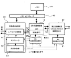
図1は、本実施形態に係る情報処理装置の概略構成を説明する図である。本実施形態に係る情報処理装置は、第1回路構成部10、第2回路構成部20および回路構成制御部30を備えている。
図2は、本実施形態に係る情報処理装置のブロック構成図である。回路構成制御部30は、情報パス制御部31、スケジューラ32および分割制御部33を備える。情報パス制御部31は、処理対象となる情報の流れを制御する。すなわち、入力された情報を第1回路構成部や第2回路構成部に送る処理や、第1回路構成部および第2回路構成部とメモリとの間の情報の入出力を制御する。情報パス制御部31は、第1回路構成部10との間で情報の入出力を行う際、第1回路構成部10にトリガーTrg1を送る。また、第2回路構成部20との間で情報の入出力を行う際、第2回路構成部20にトリガーTrg2を送る。
[パイプライン]
図3は、情報処理のパイプラインを説明する図である。ここでは、情報処理として画像処理を例とし、1ピクセル(画素)ごと所定の画像処理を施す回路を例としている。また、図中「Config」は所定の処理回路の構成を示している。図3に示す例では、「Config−1」〜「Config−5」による回路構成が成され、「Config−1」〜「Config−4」が1ピクセル当たり1クロックでの処理、「Config−5」が1ピクセル当たり4クロックでの処理となっている。
図4(a)は、パイプライン管理テーブルの例を示す図である。先に説明した画像情報のパイプライン処理を行うにあたり、スケジューラは図4(a)に示すパイプライン管理テーブルを用いて第1回路構成部の回路構成を行う。パイプライン管理テーブルには、回路構成であるConfig No.に対応して、使用するプロセッサエレメント(PE)の数、残りのPEの数、入力データ数(Input Stream Size)、出力データ数(OutPut Stream Size)、プロセッサタイプ、回路構成サイズ、レイテンシ(遅延クロック数)、処理時間が格納されている。スケジューラはこのパイプライン管理テーブルを参照して、回路構成の指示を行う。
図4(b)は、ロジックエレメントの(LE)の選択テーブルの例を示す図である。スケジューラは図4(b)に示す選択テーブルを用いて第2回路構成部の回路構成を行う。選択テーブルには、選択の優先順位に対応して、デバイス名、処理速度、書き換え時間、ロジックエレメント数(Gate bit)およびメモリ数が格納されている。スケジューラはこの選択テーブルを参照して、回路構成の指示を行う。すなわち、粗粒度の再構成可能回路(第1回路構成部)でレイテンシが発生する部分において、細粒度の再構成可能回路(第2回路構成部)へ置き換える場合、細粒度の再構成可能回路の候補をこのテーブルから選択する。その時にプライオリティ順に選択し、目標性能を達成するか判断する。
図5は、処理回路の構成による情報処理の流れを説明する図である。ここでは、回路構成の書き換えについて検討する。図5に示す例では、「Config−1」〜「Config−5」による回路構成が成され、「Config−1」「Config−2」「Config−4」が1ピクセル当たり1クロックでの処理、「Config−3」が1ピクセル当たり4クロックでの処理、「Config−5」が1ピクセル当たり3クロックでの処理となっている。
[第1のスケジューリング]
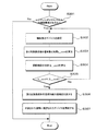
図8は、第1のスケジューリングを説明するフローチャートである。このフローチャートでの処理は、回路構成制御部30のスケジューラ32で実行される。先ず、所望の情報処理の回路構成(Config)で処理時間が所定の閾値を超えるものを抽出する(ステップS201)。回路構成の処理時間は、図4(a)に示す管理テーブルを参照することで行われる。例えば、この判断によって、回路構成中、フィードバック等の処理によって1ピクセル当たりの処理に1クロックを超えるレイテンシが発生しているものが抽出される。レイテンシが発生する回路構成(Config)が抽出されない場合は終了する。
図11は、第2のスケジューリングを説明するフローチャートであり、第2回路構成部のパーシャル リコンフィグレーション(部分再構成)機能による高速化の処理を示すものである。このフローチャートでの処理は、回路構成制御部のスケジューラで実行される。先ず、所望の情報処理の回路構成(Config)で処理時間が所定の閾値(ここでは、2クロック)以上となるものを抽出する(ステップS301)。回路構成の処理時間は、図4(a)に示す管理テーブルを参照することで行われる。例えば、この判断によって、回路構成中、フィードバック等の処理によって1ピクセル当たりの処理に2クロック以上のレイテンシが発生しているものが抽出される。レイテンシが発生する回路構成(Config)が抽出されない場合は終了する。
図14は、第3のスケジューリングを説明するフローチャートである。このフローチャートでの処理は、回路構成制御部のスケジューラで実行される。先ず、情報の入出力で依存関係のない回路構成(Config)があるか否かを判断する(ステップS401)。依存関係のない回路構成がない場合には処理を終了する。
図17は、第4のスケジューリングを説明するパイプラインの流れ図である。図17の上図は、第4のスケジューリングを行う前の流れを示す図、下図は、第4のスケジューリングを行った後の流れを示す図である。
Claims (10)
- 動的に回路が再構成される第1演算部を複数備える第1回路構成手段と、
固定の回路から成る第2演算部を複数備える第2回路構成手段と、
情報を処理するにあたり、情報処理にかかる時間に応じて前記第1回路構成手段の第1演算部による回路構成および前記第2回路構成手段の第2演算部による回路構成を制御する回路構成制御手段と
を有する情報処理装置。 - 前記第1回路構成手段による第1演算部は、前記第2回路構成手段による第2演算部より演算回路の粒度が大きい
請求項1記載の情報処理装置。 - 前記第1回路構成手段は、前記第2回路構成手段より短い時間で回路構成が変更される
請求項1または2記載の情報処理装置。 - 前記第1回路構成手段の第1演算部は複数の演算回路によって構成され、前記第2回路構成手段の第2演算部は単一の演算回路によって構成される
請求項1から3のうちいずれか1項に記載の情報処理装置。 - 前記回路構成制御手段は、一の情報の処理結果を他の情報の処理に用いない情報処理を行う際には前記第1回路構成手段の第1演算部による回路構成を制御する
請求項1から4のうちいずれか1項に記載の情報処理装置。 - 前記回路構成制御手段は、一の情報の処理結果を他の情報の処理に用いる情報処理を行う際には前記第2回路構成手段の第2演算部による回路構成を制御を行う
請求項1から5のうちいずれか1項に記載の情報処理装置。 - 前記回路構成制御手段は、前記第1回路構成手段の複数の第1演算部のうち一部を用いた回路構成を制御する
請求項1から6のうちいずれか1項に記載の情報処理装置。 - 前記回路構成制御手段は、前記第2回路構成手段の複数の第2演算部のうち一部を用いた回路構成を制御する
請求項1から7のうちいずれか1項に記載の情報処理装置。 - 前記回路構成制御手段は、前記第2回路構成手段を複数の領域に分割し、各々の領域について相異なる領域で情報処理を行っている間に自領域の回路構成を行うよう制御する
請求項1から7のうちいずれか1項に記載の情報処理装置。 - 動的に回路が再構成される第1演算部を複数備える第1回路構成手段と、固定の回路から成る第2演算部を複数備える第2回路構成手段とを用いて情報を処理するにあたり、情報処理にかかる時間に応じて前記第1回路構成手段の第1演算部による回路構成および前記第2回路構成手段の第2演算部による回路構成を制御するステップを情報処理装置に実行させる
情報処理プログラム。
Priority Applications (2)
| Application Number | Priority Date | Filing Date | Title |
|---|---|---|---|
| JP2009051638A JP5007838B2 (ja) | 2009-03-05 | 2009-03-05 | 情報処理装置および情報処理プログラム |
| US12/537,886 US20100228958A1 (en) | 2009-03-05 | 2009-08-07 | Information processing apparatus, method for controlling information processing apparatus and computer readable medium |
Applications Claiming Priority (1)
| Application Number | Priority Date | Filing Date | Title |
|---|---|---|---|
| JP2009051638A JP5007838B2 (ja) | 2009-03-05 | 2009-03-05 | 情報処理装置および情報処理プログラム |
Publications (2)
| Publication Number | Publication Date |
|---|---|
| JP2010205108A true JP2010205108A (ja) | 2010-09-16 |
| JP5007838B2 JP5007838B2 (ja) | 2012-08-22 |
Family
ID=42679266
Family Applications (1)
| Application Number | Title | Priority Date | Filing Date |
|---|---|---|---|
| JP2009051638A Expired - Fee Related JP5007838B2 (ja) | 2009-03-05 | 2009-03-05 | 情報処理装置および情報処理プログラム |
Country Status (2)
| Country | Link |
|---|---|
| US (1) | US20100228958A1 (ja) |
| JP (1) | JP5007838B2 (ja) |
Cited By (6)
| Publication number | Priority date | Publication date | Assignee | Title |
|---|---|---|---|---|
| JP2014500644A (ja) * | 2010-10-22 | 2014-01-09 | サムスン ヘビー インダストリーズ カンパニー リミテッド | 動作中に再構成可能な制御システム及びその方法 |
| US9621159B2 (en) | 2014-09-19 | 2017-04-11 | Kabushiki Kaisha Toshiba | Reconfigurable semiconductor integrated circuit and electronic device |
| JP2017204121A (ja) * | 2016-05-11 | 2017-11-16 | 富士通株式会社 | 情報処理装置、情報処理装置の制御方法および情報処理装置の制御プログラム |
| US10884794B2 (en) | 2016-08-09 | 2021-01-05 | Fujitsu Limited | Control apparatus for information processing system, computer-readable non-transitory recording medium having program stored therein, and information processing method which allocate processes executed to acquire desired result to processing apparatus to perform for pipeline processing |
| CN113128142A (zh) * | 2021-04-27 | 2021-07-16 | 北京智芯仿真科技有限公司 | 基于文件锁的集成电路电磁仿真粗颗粒并行方法及装置 |
| JP2023508503A (ja) * | 2019-12-30 | 2023-03-02 | スター アリー インターナショナル リミテッド | 構成可能な並列計算用のプロセッサ |
Families Citing this family (3)
| Publication number | Priority date | Publication date | Assignee | Title |
|---|---|---|---|---|
| JP5572527B2 (ja) * | 2010-11-09 | 2014-08-13 | パナソニック株式会社 | 通信処理装置及び通信処理方法 |
| JP6823251B2 (ja) * | 2016-10-13 | 2021-02-03 | 富士通株式会社 | 情報処理装置、情報処理方法及びプログラム |
| US12568020B2 (en) * | 2023-10-26 | 2026-03-03 | Sophos Limited | Endpoint computer configuration management |
Citations (3)
| Publication number | Priority date | Publication date | Assignee | Title |
|---|---|---|---|---|
| JPH0851355A (ja) * | 1994-06-30 | 1996-02-20 | Texas Instr Inc <Ti> | 結合された異質のフィールドプログラマブル・ゲートアレイ論理モジュールのシステムとその形成方法 |
| JP2002016489A (ja) * | 2000-06-30 | 2002-01-18 | Fuji Xerox Co Ltd | プログラマブル論理回路装置、及び情報処理システム |
| JP2006197023A (ja) * | 2005-01-11 | 2006-07-27 | Fujitsu Ltd | 半導体集積回路 |
Family Cites Families (10)
| Publication number | Priority date | Publication date | Assignee | Title |
|---|---|---|---|---|
| US5970254A (en) * | 1997-06-27 | 1999-10-19 | Cooke; Laurence H. | Integrated processor and programmable data path chip for reconfigurable computing |
| US6952828B2 (en) * | 2001-09-26 | 2005-10-04 | The Boeing Company | System, method and computer program product for dynamic resource management |
| TW200504592A (en) * | 2003-07-24 | 2005-02-01 | Ind Tech Res Inst | Reconfigurable apparatus with high hardware efficiency |
| US7584345B2 (en) * | 2003-10-30 | 2009-09-01 | International Business Machines Corporation | System for using FPGA technology with a microprocessor for reconfigurable, instruction level hardware acceleration |
| US7167971B2 (en) * | 2004-06-30 | 2007-01-23 | International Business Machines Corporation | System and method for adaptive run-time reconfiguration for a reconfigurable instruction set co-processor architecture |
| US7299339B2 (en) * | 2004-08-30 | 2007-11-20 | The Boeing Company | Super-reconfigurable fabric architecture (SURFA): a multi-FPGA parallel processing architecture for COTS hybrid computing framework |
| JP4082706B2 (ja) * | 2005-04-12 | 2008-04-30 | 学校法人早稲田大学 | マルチプロセッサシステム及びマルチグレイン並列化コンパイラ |
| US8667494B1 (en) * | 2006-08-25 | 2014-03-04 | Emc Corporation | Controlling resource allocation using thresholds and scheduling |
| US7831803B2 (en) * | 2007-07-19 | 2010-11-09 | International Business Machines Corporation | Executing multiple instructions multiple date (‘MIMD’) programs on a single instruction multiple data (‘SIMD’) machine |
| US8327126B2 (en) * | 2008-08-25 | 2012-12-04 | International Business Machines Corporation | Multicore processor and method of use that adapts core functions based on workload execution |
-
2009
- 2009-03-05 JP JP2009051638A patent/JP5007838B2/ja not_active Expired - Fee Related
- 2009-08-07 US US12/537,886 patent/US20100228958A1/en not_active Abandoned
Patent Citations (3)
| Publication number | Priority date | Publication date | Assignee | Title |
|---|---|---|---|---|
| JPH0851355A (ja) * | 1994-06-30 | 1996-02-20 | Texas Instr Inc <Ti> | 結合された異質のフィールドプログラマブル・ゲートアレイ論理モジュールのシステムとその形成方法 |
| JP2002016489A (ja) * | 2000-06-30 | 2002-01-18 | Fuji Xerox Co Ltd | プログラマブル論理回路装置、及び情報処理システム |
| JP2006197023A (ja) * | 2005-01-11 | 2006-07-27 | Fujitsu Ltd | 半導体集積回路 |
Cited By (7)
| Publication number | Priority date | Publication date | Assignee | Title |
|---|---|---|---|---|
| JP2014500644A (ja) * | 2010-10-22 | 2014-01-09 | サムスン ヘビー インダストリーズ カンパニー リミテッド | 動作中に再構成可能な制御システム及びその方法 |
| US9621159B2 (en) | 2014-09-19 | 2017-04-11 | Kabushiki Kaisha Toshiba | Reconfigurable semiconductor integrated circuit and electronic device |
| JP2017204121A (ja) * | 2016-05-11 | 2017-11-16 | 富士通株式会社 | 情報処理装置、情報処理装置の制御方法および情報処理装置の制御プログラム |
| US10884794B2 (en) | 2016-08-09 | 2021-01-05 | Fujitsu Limited | Control apparatus for information processing system, computer-readable non-transitory recording medium having program stored therein, and information processing method which allocate processes executed to acquire desired result to processing apparatus to perform for pipeline processing |
| JP2023508503A (ja) * | 2019-12-30 | 2023-03-02 | スター アリー インターナショナル リミテッド | 構成可能な並列計算用のプロセッサ |
| JP7765389B2 (ja) | 2019-12-30 | 2025-11-06 | スター アリー インターナショナル リミテッド | 構成可能な並列計算用のプロセッサ |
| CN113128142A (zh) * | 2021-04-27 | 2021-07-16 | 北京智芯仿真科技有限公司 | 基于文件锁的集成电路电磁仿真粗颗粒并行方法及装置 |
Also Published As
| Publication number | Publication date |
|---|---|
| JP5007838B2 (ja) | 2012-08-22 |
| US20100228958A1 (en) | 2010-09-09 |
Similar Documents
| Publication | Publication Date | Title |
|---|---|---|
| JP5007838B2 (ja) | 情報処理装置および情報処理プログラム | |
| US7953956B2 (en) | Reconfigurable circuit with a limitation on connection and method of determining functions of logic circuits in the reconfigurable circuit | |
| US9323716B2 (en) | Hierarchical reconfigurable computer architecture | |
| US7120903B2 (en) | Data processing apparatus and method for generating the data of an object program for a parallel operation apparatus | |
| US11171652B2 (en) | Method and apparatus for implementing configurable streaming networks | |
| KR20030064239A (ko) | 화상을 처리하는 장치 및 방법과 이 장치에 이용되는컴파일러 | |
| EP3384498B1 (en) | Shift register with reduced wiring complexity | |
| WO2018067251A1 (en) | Methods and apparatus for dynamically configuring soft processors on an integrated circuit | |
| JP4484756B2 (ja) | リコンフィギュラブル回路および処理装置 | |
| US9773083B1 (en) | Post-placement and pre-routing processing of critical paths in a circuit design | |
| JP4907521B2 (ja) | 再構成可能な半導体集積回路及びその処理割り当て方法 | |
| US20100174884A1 (en) | Processor having reconfigurable arithmetic element | |
| Chen et al. | Configuration-sensitive process scheduling for FPGA-based computing platforms | |
| US7146480B2 (en) | Configurable memory system | |
| JP4743581B2 (ja) | データ処理システムおよびその制御方法 | |
| JP4553615B2 (ja) | 処理装置 | |
| JP4562678B2 (ja) | データフローグラフ再構成装置、リコンフィギュラブル回路の設定データ生成装置、及び処理装置 | |
| JP3989397B2 (ja) | 集積回路装置およびその装置に対するデータ設定装置 | |
| JP4562679B2 (ja) | データフローグラフ生成装置 | |
| Gu et al. | Efficient algorithms for 2D area management and online task placement on runtime reconfigurable FPGAs | |
| JP2008219728A (ja) | 再構成可能な演算処理回路 | |
| JP6349995B2 (ja) | データ処理装置 | |
| JP4610236B2 (ja) | 設定データ生成装置 | |
| Jayasinghe et al. | Two-level pipelined systolic array graphics engine | |
| JP2010033336A (ja) | 信号処理装置及び信号処理方法 |
Legal Events
| Date | Code | Title | Description |
|---|---|---|---|
| A131 | Notification of reasons for refusal |
Free format text: JAPANESE INTERMEDIATE CODE: A131 Effective date: 20110301 |
|
| A521 | Written amendment |
Free format text: JAPANESE INTERMEDIATE CODE: A523 Effective date: 20110427 |
|
| A131 | Notification of reasons for refusal |
Free format text: JAPANESE INTERMEDIATE CODE: A131 Effective date: 20120130 |
|
| A521 | Written amendment |
Free format text: JAPANESE INTERMEDIATE CODE: A523 Effective date: 20120327 |
|
| TRDD | Decision of grant or rejection written | ||
| A01 | Written decision to grant a patent or to grant a registration (utility model) |
Free format text: JAPANESE INTERMEDIATE CODE: A01 Effective date: 20120502 |
|
| A01 | Written decision to grant a patent or to grant a registration (utility model) |
Free format text: JAPANESE INTERMEDIATE CODE: A01 |
|
| A61 | First payment of annual fees (during grant procedure) |
Free format text: JAPANESE INTERMEDIATE CODE: A61 Effective date: 20120515 |
|
| R150 | Certificate of patent or registration of utility model |
Free format text: JAPANESE INTERMEDIATE CODE: R150 |
|
| FPAY | Renewal fee payment (event date is renewal date of database) |
Free format text: PAYMENT UNTIL: 20150608 Year of fee payment: 3 |
|
| LAPS | Cancellation because of no payment of annual fees |