JP2010232425A - Semiconductor laser element and method for manufacturing the same - Google Patents
Semiconductor laser element and method for manufacturing the same Download PDFInfo
- Publication number
- JP2010232425A JP2010232425A JP2009078362A JP2009078362A JP2010232425A JP 2010232425 A JP2010232425 A JP 2010232425A JP 2009078362 A JP2009078362 A JP 2009078362A JP 2009078362 A JP2009078362 A JP 2009078362A JP 2010232425 A JP2010232425 A JP 2010232425A
- Authority
- JP
- Japan
- Prior art keywords
- semiconductor laser
- reflective film
- active layer
- laser device
- layer
- Prior art date
- Legal status (The legal status is an assumption and is not a legal conclusion. Google has not performed a legal analysis and makes no representation as to the accuracy of the status listed.)
- Pending
Links
- 239000004065 semiconductor Substances 0.000 title claims abstract description 103
- 238000004519 manufacturing process Methods 0.000 title claims abstract description 11
- 238000000034 method Methods 0.000 title abstract description 19
- 229910052984 zinc sulfide Inorganic materials 0.000 claims abstract description 10
- 230000010355 oscillation Effects 0.000 claims description 44
- 238000005253 cladding Methods 0.000 claims description 36
- 239000000758 substrate Substances 0.000 claims description 30
- 150000004767 nitrides Chemical group 0.000 claims description 24
- 238000010521 absorption reaction Methods 0.000 claims description 19
- 239000013078 crystal Substances 0.000 claims description 8
- 238000010030 laminating Methods 0.000 claims description 4
- 125000005842 heteroatom Chemical group 0.000 abstract description 3
- 239000010410 layer Substances 0.000 description 141
- 230000003287 optical effect Effects 0.000 description 17
- 238000001228 spectrum Methods 0.000 description 15
- 230000008569 process Effects 0.000 description 10
- 239000000463 material Substances 0.000 description 9
- 239000011777 magnesium Substances 0.000 description 8
- JMASRVWKEDWRBT-UHFFFAOYSA-N Gallium nitride Chemical compound [Ga]#N JMASRVWKEDWRBT-UHFFFAOYSA-N 0.000 description 7
- 230000005684 electric field Effects 0.000 description 7
- 230000001681 protective effect Effects 0.000 description 7
- IJGRMHOSHXDMSA-UHFFFAOYSA-N Atomic nitrogen Chemical compound N#N IJGRMHOSHXDMSA-UHFFFAOYSA-N 0.000 description 6
- KRHYYFGTRYWZRS-UHFFFAOYSA-N Fluorane Chemical compound F KRHYYFGTRYWZRS-UHFFFAOYSA-N 0.000 description 6
- 229910004298 SiO 2 Inorganic materials 0.000 description 5
- 238000000151 deposition Methods 0.000 description 5
- 239000002994 raw material Substances 0.000 description 5
- XCZXGTMEAKBVPV-UHFFFAOYSA-N trimethylgallium Chemical compound C[Ga](C)C XCZXGTMEAKBVPV-UHFFFAOYSA-N 0.000 description 5
- NBIIXXVUZAFLBC-UHFFFAOYSA-N Phosphoric acid Chemical compound OP(O)(O)=O NBIIXXVUZAFLBC-UHFFFAOYSA-N 0.000 description 4
- 230000015572 biosynthetic process Effects 0.000 description 4
- 230000000052 comparative effect Effects 0.000 description 4
- 230000007423 decrease Effects 0.000 description 4
- 238000005530 etching Methods 0.000 description 4
- 229910052733 gallium Inorganic materials 0.000 description 4
- 229910052738 indium Inorganic materials 0.000 description 4
- JLTRXTDYQLMHGR-UHFFFAOYSA-N trimethylaluminium Chemical compound C[Al](C)C JLTRXTDYQLMHGR-UHFFFAOYSA-N 0.000 description 4
- 229910002704 AlGaN Inorganic materials 0.000 description 3
- 229910052782 aluminium Inorganic materials 0.000 description 3
- 230000004888 barrier function Effects 0.000 description 3
- 230000008859 change Effects 0.000 description 3
- 230000008021 deposition Effects 0.000 description 3
- 239000002019 doping agent Substances 0.000 description 3
- 230000000694 effects Effects 0.000 description 3
- 238000001451 molecular beam epitaxy Methods 0.000 description 3
- 229910052757 nitrogen Inorganic materials 0.000 description 3
- QJGQUHMNIGDVPM-UHFFFAOYSA-N nitrogen(.) Chemical compound [N] QJGQUHMNIGDVPM-UHFFFAOYSA-N 0.000 description 3
- 230000010287 polarization Effects 0.000 description 3
- QAOWNCQODCNURD-UHFFFAOYSA-N Sulfuric acid Chemical compound OS(O)(=O)=O QAOWNCQODCNURD-UHFFFAOYSA-N 0.000 description 2
- 229910000147 aluminium phosphate Inorganic materials 0.000 description 2
- 239000000969 carrier Substances 0.000 description 2
- 210000004027 cell Anatomy 0.000 description 2
- 230000031700 light absorption Effects 0.000 description 2
- 229910052751 metal Inorganic materials 0.000 description 2
- 239000002184 metal Substances 0.000 description 2
- 239000003960 organic solvent Substances 0.000 description 2
- 239000012071 phase Substances 0.000 description 2
- 210000004180 plasmocyte Anatomy 0.000 description 2
- 229910052710 silicon Inorganic materials 0.000 description 2
- 239000010703 silicon Substances 0.000 description 2
- 230000007704 transition Effects 0.000 description 2
- IBEFSUTVZWZJEL-UHFFFAOYSA-N trimethylindium Chemical compound C[In](C)C IBEFSUTVZWZJEL-UHFFFAOYSA-N 0.000 description 2
- XLYOFNOQVPJJNP-UHFFFAOYSA-N water Substances O XLYOFNOQVPJJNP-UHFFFAOYSA-N 0.000 description 2
- UFHFLCQGNIYNRP-UHFFFAOYSA-N Hydrogen Chemical compound [H][H] UFHFLCQGNIYNRP-UHFFFAOYSA-N 0.000 description 1
- BLRPTPMANUNPDV-UHFFFAOYSA-N Silane Chemical compound [SiH4] BLRPTPMANUNPDV-UHFFFAOYSA-N 0.000 description 1
- 230000005540 biological transmission Effects 0.000 description 1
- 239000012159 carrier gas Substances 0.000 description 1
- 238000003776 cleavage reaction Methods 0.000 description 1
- 230000003247 decreasing effect Effects 0.000 description 1
- 238000001312 dry etching Methods 0.000 description 1
- 238000010894 electron beam technology Methods 0.000 description 1
- 238000011156 evaluation Methods 0.000 description 1
- 239000007789 gas Substances 0.000 description 1
- 239000001257 hydrogen Substances 0.000 description 1
- 229910052739 hydrogen Inorganic materials 0.000 description 1
- 239000007788 liquid Substances 0.000 description 1
- 238000001459 lithography Methods 0.000 description 1
- QBJCZLXULXFYCK-UHFFFAOYSA-N magnesium;cyclopenta-1,3-diene Chemical compound [Mg+2].C1C=CC=[C-]1.C1C=CC=[C-]1 QBJCZLXULXFYCK-UHFFFAOYSA-N 0.000 description 1
- 238000000206 photolithography Methods 0.000 description 1
- 239000011241 protective layer Substances 0.000 description 1
- 230000009467 reduction Effects 0.000 description 1
- 238000012827 research and development Methods 0.000 description 1
- 230000007017 scission Effects 0.000 description 1
- 229910000077 silane Inorganic materials 0.000 description 1
- 238000001771 vacuum deposition Methods 0.000 description 1
- 238000000927 vapour-phase epitaxy Methods 0.000 description 1
- 238000005406 washing Methods 0.000 description 1
Images


Landscapes
- Semiconductor Lasers (AREA)
Abstract
Description
本発明は、半導体レーザ素子およびその製造方法に関する。 The present invention relates to a semiconductor laser device and a manufacturing method thereof.
III族窒化物半導体材料は、禁制帯幅が充分大きく、バンド間遷移も直接遷移型であるため、短波長発光素子への適用が盛んに検討されている。特に、1990年代半ば頃から、照明や各種ディスプレイ用途に、本材料を用いた紫外から青、緑色の波長領域の発光ダイオード(LED:Light Emitting Diode)の性能が急激に向上した。その結果、本材料を用いたLEDの適用範囲は格段に広がり非常に大きな市場を形成している。また、本材料は次世代の高密度光ディスク用光源としても重要である。そのため、発振波長405nmの半導体レーザダイオード(LD:Laser Diode)の研究開発が精力的に進められ、既に製品化も始まっている。 The group III nitride semiconductor material has a sufficiently large forbidden band width and a direct transition type between band transitions. Therefore, application to a short wavelength light emitting element has been actively studied. In particular, since the middle of the 1990s, the performance of light emitting diodes (LEDs) in the ultraviolet, blue, and green wavelength regions using this material for lighting and various display applications has improved dramatically. As a result, the application range of LEDs using this material has been greatly expanded to form a very large market. This material is also important as a light source for next-generation high-density optical disks. Therefore, research and development of a semiconductor laser diode (LD) with an oscillation wavelength of 405 nm has been vigorously advanced, and commercialization has already started.
また、本材料を用いたLDは投射型ディスプレイ等の光源としても検討されている。例えば、特許文献1に開示されているGaN基板上のインナーストライプ型レーザ構造により、良好なレーザ発振特性が得られている。
LDs using this material are also being studied as light sources for projection displays and the like. For example, good laser oscillation characteristics are obtained by the inner stripe laser structure on the GaN substrate disclosed in
また、本発明の関連技術として、特許文献2を挙げることができる。特許文献2では、従来のエアリッジ型GaN系半導体レーザ素子よりも閾値電流値が低く、かつ動作電圧の低いエアリッジ型GaN系半導体レーザ素子が記載されている。
Further,
また、本発明の関連技術として、特許文献3を挙げることができる。特許文献3では、発振光の光エネルギーよりも大きなバンドギャップを有する保護層をレーザ端面に設けることが記載されている。これにより、高出力発信時においても高信頼性の超寿命の窒化物半導体レーザ装置を得ることができることが記載されている。また、保護層の厚みをλ/4nの奇数倍とすることで反射層をかねてもよいことが記載されている。 Further, Patent Document 3 can be cited as a related technique of the present invention. Patent Document 3 describes that a protective layer having a band gap larger than the optical energy of oscillation light is provided on the laser end face. Thus, it is described that a highly reliable and long-life nitride semiconductor laser device can be obtained even during high-power transmission. Further, it is described that the reflective layer may serve as an odd multiple of λ / 4n.
また、本発明の関連技術として、特許文献4を挙げることができる。特許文献4では、共振器面において、保護膜を窒化物半導体層に接触させ、かつ、この保護膜と異なる結晶構造からなる保護膜を共振器面から基板の第二主面に接触するように形成することにより、保護膜の共振器面への密着性を向上させることができることが記載されている。また、保護膜は、共振器面と同軸方向の窒化膜とすることで保護膜と共振器面との密着性を高めることができることが記載されている。そして、共振器面は、M面(1−100)、A面(11−20)、C面(0001)又はR面(1−102)からなる群から選ばれる面、特にM軸配向が好ましいことが記載されている。 Further, Patent Document 4 can be cited as a related technique of the present invention. In Patent Document 4, a protective film is brought into contact with the nitride semiconductor layer on the resonator surface, and a protective film having a crystal structure different from the protective film is brought into contact with the second main surface of the substrate from the resonator surface. It is described that the adhesion of the protective film to the resonator surface can be improved by forming the protective film. Further, it is described that the adhesion between the protective film and the resonator surface can be improved by forming the protective film as a nitride film coaxial with the resonator surface. The resonator plane is preferably a plane selected from the group consisting of M-plane (1-100), A-plane (11-20), C-plane (0001), or R-plane (1-102), particularly M-axis orientation. It is described.
しかしながら、特許文献1〜4に記載の半導体レーザをディスプレイ用光源として用いる場合、レーザ光の可干渉性が原因で発生する「ちらつき」すなわちスペックルノイズの低減が重要な課題となる。従来は、このスペックルノイズを低減するために複数の独立したレーザ光を重ね合わせたり、時空間的に位相を変化させるための光学素子を用いる必要があり、光源の小型化や低コスト化が困難であった。
However, when the semiconductor laser described in
本発明は、スペックルノイズが低減され、小型、低コストかつ高性能な半導体レーザ素子及びその製造方法を提供することを目的とする。 SUMMARY OF THE INVENTION An object of the present invention is to provide a small-sized, low-cost and high-performance semiconductor laser device with reduced speckle noise and a method for manufacturing the same.
本発明によれば、
第一のクラッド層と活性層と第二のクラッド層とを順に積層したダブルヘテロ構造部と、
前記活性層を挟んで形成された一対の共振器端面と、
少なくとも一の前記共振器端面に形成され、前記共振器端面から発振される発振光を吸収する反射膜と、
を備え、
少なくとも前記活性層及び前記反射膜がウルツ鉱型半導体からなり、
前記共振器端面が、極性を有する面に形成され、
前記活性層のバンドギャップをEgavとし、前記反射膜のバンドギャップをEgrとしたとき、下記式(1)を満たす、半導体レーザ素子が提供される。
(1)1×Egr≦Egav≦1.2×Egr
According to the present invention,
A double heterostructure part in which a first cladding layer, an active layer, and a second cladding layer are sequentially stacked;
A pair of resonator end faces formed across the active layer;
A reflective film that is formed on at least one of the resonator end faces and absorbs oscillation light oscillated from the resonator end faces;
With
At least the active layer and the reflective film are made of a wurtzite semiconductor,
The resonator end surface is formed on a surface having polarity,
Provided is a semiconductor laser device that satisfies the following formula (1), where Eg av is the band gap of the active layer and Eg r is the band gap of the reflective film.
(1) 1 × Eg r ≦ Eg av ≦ 1.2 × Eg r
また、本発明によれば、
第一のクラッド層と活性層と第二のクラッド層とを順に積層する工程と、
前記活性層を挟む一対の共振器端面を形成する工程と、
前記共振器端面から発振される発振光を吸収する反射膜を少なくとも一の前記共振器端面に積層する工程と、
を含み、
少なくとも前記活性層及び前記反射膜をウルツ鉱型半導体で形成し、
前記共振器端面を形成する前記工程において、前記共振器端面を極性を有する面に形成し、前記活性層のバンドギャップをEgavとし、前記反射膜のバンドギャップをEgrとしたとき、下記式(1)を満たす、半導体レーザ素子の製造方法が提供される。
(1)1×Egr≦Egav≦1.2×Egr
Moreover, according to the present invention,
Laminating a first cladding layer, an active layer, and a second cladding layer in order;
Forming a pair of resonator end faces sandwiching the active layer;
Laminating a reflection film that absorbs oscillation light oscillated from the resonator end face on at least one of the resonator end faces;
Including
At least the active layer and the reflective film are formed of a wurtzite semiconductor,
In the step of forming the cavity end face, the cavity end face formed on the surface having a polarity, the band gap of the active layer and Eg av, when the band gap of the reflective film and Eg r, the following equation A method of manufacturing a semiconductor laser device that satisfies (1) is provided.
(1) 1 × Eg r ≦ Eg av ≦ 1.2 × Eg r
本発明によれば、スペックルノイズが低減され、小型、低コストかつ高性能な半導体レーザ素子及びその製造方法を提供することができる。 According to the present invention, it is possible to provide a small-sized, low-cost and high-performance semiconductor laser device with reduced speckle noise and a manufacturing method thereof.
以下、本発明の実施の形態について、図面を用いて説明する。尚、すべての図面において、同様な構成要素には同様の符号を付し、適宜説明を省略する。 Hereinafter, embodiments of the present invention will be described with reference to the drawings. In all the drawings, the same reference numerals are given to the same components, and the description will be omitted as appropriate.
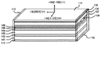
図1は、本実施形態の半導体レーザ素子を示す模式的な斜視断面図である。この半導体レーザ素子は、n型クラッド層103(第一のクラッド層)と活性層105とp型クラッド層109(第二のクラッド層)とを順に積層したダブルヘテロ構造部と、活性層105を挟んで形成された一対のレーザ共振器端面と、レーザ共振器端面に形成され、レーザ共振器端面から発振される発振光を吸収する反射膜113と、を備えている。この半導体レーザ素子は、ウルツ鉱型半導体からなる。レーザ共振器端面は、C面(0001)に形成されている。活性層105のバンドギャップをEgavとし、反射膜113のバンドギャップをEgrとしたとき、下記式(1)を満たす。
(1)1×Egr≦Egav≦1.2×Egr
FIG. 1 is a schematic perspective sectional view showing the semiconductor laser device of the present embodiment. This semiconductor laser element includes a double heterostructure part in which an n-type cladding layer 103 (first cladding layer), an
(1) 1 × Eg r ≦ Eg av ≦ 1.2 × Eg r
本実施形態の半導体レーザ素子は、n型基板101(半導体基板)の{1−100}面(m面、無極性面)上に作製する。反射膜113は、ウルツ鉱型半導体からなり、共振器方向、すなわち、C軸方向[0001]方向に積層されている。そのため、発振光を吸収していない状態1の反射膜113は、ピエゾ電界により共振器方向に分極電場を有する。そして、反射膜113は、このピエゾ電界により、反射膜113を構成する材料のバンドギャップよりも反射膜113のバンドギャップが縮小されるように設計されている。
The semiconductor laser device of this embodiment is fabricated on the {1-100} plane (m-plane, nonpolar plane) of the n-type substrate 101 (semiconductor substrate). The
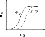
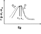
この素子は、活性層105及び反射膜113のバンドギャップが上記式(1)を満たす。これにより、レーザ発振が開始する前の初期状態において、反射膜113の吸収端波長と発振光の波長とが略同一となる。したがって、共振器端面から光が発振されると、反射膜113は発振光の一部を吸収する。これにより、反射膜113内に励起キャリアが発生し、励起キャリアの密度の上昇に応じて、内部電界がスクリーニング(遮蔽)されることになる。したがって、バンドギャップエネルギーが大きくなり、反射膜113のミラーロスαmが減少し(図2中破線2)、素子から出射されるレーザ光の波長は長波になる(図3破線2)。一方、発振光を吸収している状態2の反射膜113は、バンドギャップエネルギーが大きくなることで、吸収端波長が短くなり、活性層105からの発振光の吸収量が小さくなる。これにより、反射膜113におけるキャリア密度が徐々に減少し、内部電界がスクリーニング(遮蔽)されなくなる。その結果、反射膜113のバンドギャップエネルギーが小さくなり、ミラーロスαmが増加して状態1の反射膜113のミラーロスと同じになる(図2中実線1)。したがって、レーザ素子から出射されるレーザ光の波長は短波になる(図3実線1)。以降周期的に、状態1と状態2との間で変動し、ミラーロススペクトルが状態1と状態2との間で変動する。このように、発振光が照射されることにより反射膜113は振動する。
In this element, the band gap between the
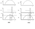
以下、図2〜5を用いて本実施形態の半導体レーザの原理についてさらに詳細に説明する。図2、5(c)(d)は、反射膜113のミラーロススペクトルを有している。図2において、横軸は反射膜113が吸収した光のエネルギー(Eg)を示す。図5(c)、(d)において、横軸は反射膜113の吸収端波長(λ)を示す。図3、5(e)(f)は、本実施形態の半導体レーザのゲインスペクトルを有している。図3において、横軸は出射光のエネルギー(Eg)を示し、図5(e)、(f)において、横軸は出射光の波長(λ)を示す。図4、5(a)、(b)は、活性層105のネットゲインスペクトルを有している。図4において、横軸は発振光のエネルギー(Eg)を示し、図5(a)、(b)において、横軸は発振光の波長(λ)を示す。図5(a)、(c)、(e)は、反射膜113が発振光を吸収していない第一状態を示し、図5(b)、(d)、(f)は、反射膜113が発振光を吸収した第二状態を示す。
Hereinafter, the principle of the semiconductor laser according to the present embodiment will be described in more detail with reference to FIGS. 2, 5 (c) and (d) have the mirror loss spectrum of the
ネットゲインG’は下記式(1)で定義される。
G’=Γ×g−αi(1)
但し、Γは活性層105の閉込係数、gは利得係数(cm−1)、αiは半導体レーザ素子の全損失に対する吸収係数(cm−1)である。
The net gain G ′ is defined by the following formula (1).
G ′ = Γ × g−α i (1)
Where Γ is a confinement factor of the
ゲインGは下記式(2)で定義される。
G=G’−αm(2)
The gain G is defined by the following formula (2).
G = G′−α m (2)
図4、図5(a)、(b)で示すように、活性層105のネットゲインスペクトルは、状態1と状態2との間で変化しない。換言すると、光の発振前後において、活性層105のバンドギャップは変化しない。
As shown in FIGS. 4, 5 (a) and 5 (b), the net gain spectrum of the
この素子は、活性層105及び反射膜113のバンドギャップが上記式(1)を満たす。したがって、反射膜113の吸収端波長と活性層105の発振光の波長とが略同一となるように設計されている。略同一とは、反射膜113の吸収端波長AEと発振光の波長γとが、1/AE≦1/γ≦1.2/AEを満たすようにすると好ましく、1/AE≦1/γ≦1.1/AEを満たすようにするとより好ましい。活性層105及び反射膜113の材料が同一の元素からなると、活性層105及び反射膜113のバンドギャップを容易に上記式(1)を満たすようにすることができる。また、反射膜113は、発振光を吸収することで、ピエゾ電界が遮蔽され、バンドギャップエネルギーが上昇するように設計されている。そのため、図2で示すように、状態2では、ミラーロススペクトルが高エネルギー側にシフトとする。一方、前述のように、ネットゲインスペクトルは光の発振前後で変化しない。そのため、図3で示すように、ゲインスペクトルは、低エネルギー側にシフトする。したがって、レーザ発振直後には波長λ1でレーザ光を出射するが(図5(e)、図3中実線1)、反射膜113が波長λ1の発振光を吸収することで、波長がより長波のλ2(λ1<λ2)で出射する(図5(f)、図3中破線2)。
In this element, the band gap between the
図5(d)で示すように、状態2では、吸収端波長AE2が状態1の吸収端波長AE1よりも短い。そのため、状態2の反射膜113では、発振光の吸収量が小さくなり、励起キャリア密度が低下する。その結果、ピエゾ電界が遮蔽されなくなり、これにより、反射膜113のバンドギャップが縮小し、反射膜113のミラーロススペクトルは再び低エネルギー側に戻る(状態1、図2実線1)。これにより、ゲインスペクトルが高エネルギー側にシフトし、出射光の波長がλ1にシフトする(図3実線1)。以降周期的に、状態1と状態2との間で変動し、出射されるレーザ光の波長がλ1とλ2との間で変動する。
As shown in FIG. 5 (d), the In
以上のように出射光の波長のスイッチングを発生させるためには、下記式(3)を満たすように、出射光の波長λ及び反射膜の吸収端AEを設計する。 In order to generate the switching of the wavelength of the emitted light as described above, the wavelength λ of the emitted light and the absorption edge AE of the reflective film are designed so as to satisfy the following formula (3).
λ1<AE2≦λ2<AE1(3) λ 1 <AE 2 ≦ λ 2 <AE 1 (3)
AE1とλ2との差(Δw)は、5nm〜50nmとすると好ましい。また、λ1とλ2との差(Δλ)は、5nm〜20nmとすると好ましく、10nmが特に好ましい。また、波長の変動周期としてはおよそ数MHzから数十MHz程度であり、このときレーザ光の強度も同時に変調されてもよい。こうすることで、スペックルノイズを効果的に抑制することができる。 The difference (Δw) between AE 1 and λ 2 is preferably 5 nm to 50 nm. The difference (Δλ) between λ 1 and λ 2 is preferably 5 nm to 20 nm, and particularly preferably 10 nm. Further, the wavelength variation period is about several MHz to several tens of MHz, and at this time, the intensity of the laser beam may be modulated simultaneously. By doing so, speckle noise can be effectively suppressed.
本実施形態の半導体レーザ素子を構成するウルツ鉱型半導体としては、III族窒化物半導体またはII族酸化物半導体を用いることができ、材料の組成を任意に選択することで目的の発振波長を得ることができる。特に、III族窒化物半導体が効率よく発光できる点でより好ましい。III族窒化物半導体としては、一般式InxAlyGa(1−x−y)N(0≦x≦1、0≦y≦1、0≦x+y≦1)のものを用いることができる。また、クラッド層103、109と活性層105とを含むダブルヘテロ構造部及び反射膜113の組成や厚みをそれぞれ変更することで、活性層105の発振波長と反射膜の吸収端波長とを制御することができる。たとえば、InzGa1−zNでは、下記式(4)を用いてバンドギャップエネルギーを所望のものにすることができる(phys.stat.sol.(b)230,No2,R4−R6(2002))。
Eg(z)=3.493−2.843z−2.5×(1−z)(4)
ただし、本実施形態では、反射膜113の吸収端波長は、ピエゾ電界の影響も考慮して設計する。
As the wurtzite type semiconductor constituting the semiconductor laser device of this embodiment, a group III nitride semiconductor or a group II oxide semiconductor can be used, and a desired oscillation wavelength can be obtained by arbitrarily selecting the composition of the material. be able to. In particular, the group III nitride semiconductor is more preferable in that it can emit light efficiently. As the group III nitride semiconductor, one having a general formula of In x Al y Ga (1-xy) N (0 ≦ x ≦ 1, 0 ≦ y ≦ 1, 0 ≦ x + y ≦ 1) can be used. Further, the oscillation wavelength of the
Eg (z) = 3.493-2.843z−2.5 × (1-z) (4)
However, in this embodiment, the absorption edge wavelength of the
また、反射膜113及び活性層105を構成する元素を同一とすることで、反射膜113の吸収端波長と発振波長とをより精度よく制御することができる。たとえば、反射膜113及び活性層105をInzGa1−zN(0<z<1)からなる層とすることで、青〜緑色帯で効率的に発光するレーザを得ることができる。
Further, by making the elements constituting the
反射膜113は単結晶とすると好ましい。こうすることで、反射膜113の吸収端波長を精度よく制御することができる。
The
反射膜113は、シリコンドープしてもよい。こうすることで、吸収端波長の変動幅の制御を容易にすることができる。ドープするシリコン量は、1×10¹⁶〜1×1020cm−3とすると好ましい。
The
反射膜113は、ヘテロ構造を有することが好ましい。屈折率の差の大きい構造とすることで、反射膜113の反射率を大きくすることができる。したがって、出射するレーザ光の波長をより精度よく制御することが可能になる。反射率は80〜99%とすると好ましい。
The
反射膜113及び活性層105をInzGa1−zN(0<z<1)及びAlnGa1−nN(0<n<1)で構成することで、スペックルノイズを効果的に低減された、青〜緑色帯で発光するレーザを作製することができる。
By constructing the
つづいて、本実施形態の半導体レーザ素子の一例として、窒化物半導体レーザ素子を例に挙げて図1を用いつつ以下に説明する。この窒化物半導体レーザ素子は、n型GaN基板101と、n側バッファ層102と、n型クラッド層103と、n型光閉じ込め層104と、量子井戸層(活性層)105と、p型光閉じ込め層106と、電流狭窄層107と、p型クラッド層109と、p側コンタクト層110と、p型電極111と、n型電極112とを有する。また、レーザ共振器端面には反射膜113を有する。
Subsequently, as an example of the semiconductor laser element of the present embodiment, a nitride semiconductor laser element will be described as an example and will be described below with reference to FIG. This nitride semiconductor laser device includes an n-
図1に示すように、n型GaN基板101の主面は(1−100)面であり、<0001>方向に共振器が形成されている。さらにレーザ共振器端面は{0001}面であり、へき開又はドライエッチング等によって出射するレーザ光(発振光)と垂直に形成されている。
As shown in FIG. 1, the main surface of the n-
次に、この窒化物半導体レーザ素子の層構造についてさらに詳しく説明する。n型GaN基板101上に、n側バッファ層102が形成されている。n側バッファ層102は、例えば、Siドープn型GaN(Si濃度4×1017cm−3、厚さ1μm=1000nm)からなる。
Next, the layer structure of the nitride semiconductor laser device will be described in more detail. An n-
Siドープn型GaNバッファ層102を覆うように、n型クラッド層103が形成されている。n型クラッド層103は、例えば、Siドープn型Al0.07Ga0.93N(Si濃度4×1017cm−3、厚さ2μm=2000nm)からなる。
An n-
n型クラッド層103を覆うように、n型光閉じ込め層104が形成されている。n型光閉じ込め層104は、例えば、Siドープn型GaN(Si濃度4×1017cm−3、厚さ100nm)からなる。
An n-type
n型光閉じ込め層104を覆うように、量子井戸層105が形成されている。量子井戸層105は、例えば、In0.17Ga0.83N(厚さ3nm)井戸層とアンドープGaN(厚さ10nm)バリア層からなる2周期多重量子井戸(MQW:Multi−Quantum Well)層である。
A
量子井戸層105を覆うように、キャップ層(不図示)及びp型光閉じ込め層106が形成されている。キャップ層は、例えば、Mgドープp型Al0.2Ga0.8Nからなる。また、p型光閉じ込め層106は、例えば、Mgドープp型GaN(Mg濃度1×1019cm−3、厚さ100nm)からなる。
A cap layer (not shown) and a p-type
そして、p型光閉じ込め層106を覆うように、電流狭窄層107が形成されている。電流狭窄層107は、例えば、AlNからなる。
A
電流狭窄層107を覆うようにp型クラッド層109が形成されている。p型クラッド層109は、例えば、Mgドープp型Al0.07Ga0.93N(Mg濃度1×1019cm−3、厚さ500nm)からなる。
A p-
p型クラッド層109を覆うようにp側コンタクト層110が形成されている。p側コンタクト層110は、例えば、Mgドープp型GaN(Mg濃度2×1020cm−3以下、厚さ20nm)からなる。そして、p側コンタクト層110の上部には、p型電極111が設けられている。また、n型GaN基板101の下部には、n型電極112が設けられている。
A p-
さらにレーザ共振器端面には反射膜113が形成されている。反射膜113は、例えばIn0.12Ga0.88N(厚さ40nm)/Al0.28Ga0.72N(厚さ47nm)8周期からなる。
Further, a
つづいて、本実施形態の半導体レーザ素子の製造方法について説明する。まず、n型クラッド層103と活性層105とp型クラッド層109とを基板101の無極性面(たとえば、(1−100)面に順に積層し、ダブルヘテロ構造を形成する。
Next, a method for manufacturing the semiconductor laser device of this embodiment will be described. First, the n-
このとき、n型クラッド層103と活性層105との間にn型光閉じ込め層104を形成してもよい。また、活性層105とp型クラッド層109との間に、p型光閉じ込め層106と電流狭窄層107とを形成してもよい。
At this time, an n-type
電流狭窄層107は、以下の工程により形成することができる。まず、低温堆積により非結晶層を形成する。その後、エッチングにより、非結晶層にストライプ状の開口部を設ける。開口部は、光露光又は電子線露光などのリソグラフィーと、例えば、特許文献1に記載されている燐酸系含有液等を用いた選択エッチングとにより形成することができる。その後、非結晶層形成温度よりも高い温度でp型クラッド層109及びこれより上層を形成する。こうすることで、電流狭窄層107を非結晶層から結晶層へ変換することができる。このとき、開口部はp型クラッド層109で埋め込まれるが、製造工程の説明の便宜上、開口部であった部分を区別して埋込部108という。
The
ついで、ダブルヘテロ構造の上部にp型電極111を形成し、基板101のダブルヘテロ構造が形成された面と反対面にn電極112を形成する。ついで、極性を有する面(たとえば、<0001>方向)にへき開し、活性層105を挟む一対の共振器端面を形成する。
Next, a p-
ついで、反射膜113を共振器端面に積層する。反射膜113は、たとえば、分子線エピタキシー(MBE:Molecular Beam Epitaxy)法により形成することができる。InxAlyGa(1−x−y)N(0≦x≦1、0≦y≦1、0≦x+y≦1)からなる窒化物半導体からなる反射膜113を形成する場合、Ga、In、Alの原料には各メタルを通常のエフージョンセルを用いて分子線とし、窒素原料はRFプラズマセルにより窒素ラジカルビームとして供給する。Ga、In、Alの分子線強度及び窒素ラジカルビーム強度を調整することで、反射膜113の組成及び膜厚を制御することができる。
Next, the
つづいて、実施形態の作用効果について説明する。本実施形態では、極性を有する面に共振器端面を形成し、反射膜113をこの共振器端面上に形成し、吸収端波長を発振光の波長と略同一とする。こうすることで、反射膜113はピエゾ電界により分極電場を有し、光の吸収により分極電場をスクリーニングされることになる。そのため、発振光を吸収していない状態と発振光を吸収した状態とで反射膜113のバンドギャップを変化させることができる。さらに、反射膜113の吸収端波長が光の吸収により短波化させることにより、発振光の照射により反射膜113の吸収端波長が振動する。すなわち、反射膜113の光の吸収量を周期的に変動させることにより、反射膜113のミラーロスを周期的に変動させることができ、その結果、素子から出射されるレーザ光の波長が周期的に変動することになる。したがって、本実施形態の素子によれば、レーザ光の干渉性が低下するためスペックルノイズを低減することが可能となる。
It continues and demonstrates the effect of embodiment. In the present embodiment, the resonator end face is formed on a surface having polarity, the
また、この半導体レーザ素子では、発振光を重ね合わせたり時空間的に位相を変化させたりするための光学素子を用いずにスペックルノイズを低減できる。したがって、光源の小型化や低コスト化が可能でかつ高性能な半導体レーザ素子を実現することができる。 Further, in this semiconductor laser element, speckle noise can be reduced without using an optical element for superimposing oscillation light or changing a phase in space and time. Therefore, it is possible to realize a high-performance semiconductor laser device capable of reducing the size and cost of the light source.
以上、図面を参照して本発明の実施形態について述べたが、これらは本発明の例示であり、上記以外の様々な構成を採用することもできる。たとえば、実施形態では、反射膜は、共振器端面と同じ結晶軸方向、すなわち、C軸方向[0001]方向に配向させる例を示した。しかしながら、極性を有する面であればよく、(1−101)面や(11−22)面などの半極性面であってもよい。また、実施形態で示すように(0001)面を共振器端面として用いることで、反射膜113に良好な内部電場をかけることができるが、共振器端面は、面方位が<0001>成分を含む、半極性面または極性面であればよい。また、レーザ端面の{0001}面以外の{0001}面とのなす角が90度未満の半極性面としてもよい。n型をp型としてもよくp型をn型としてもよい。また、実施形態では基板にダブルヘテロ構造を形成する例を挙げて説明したが、テンプレート上にダブルヘテロ構造を形成してもよい。
As mentioned above, although embodiment of this invention was described with reference to drawings, these are the illustrations of this invention, Various structures other than the above are also employable. For example, in the embodiment, an example has been described in which the reflective film is oriented in the same crystal axis direction as the resonator end face, that is, in the C-axis direction [0001] direction. However, it may be a plane having polarity, and may be a semipolar plane such as a (1-101) plane or a (11-22) plane. In addition, as shown in the embodiment, by using the (0001) plane as the resonator end surface, a good internal electric field can be applied to the
また、基板主面の面方位をm面としたが、共振器端面の面方位が<0001>成分を含む、半極性または極性面であれば、基板主面の面方位は他の面でも本発明の効果を得ることができる。したがって、基板主面を{0001}面(c面)、レーザ端面もc面で構成される面発光レーザの場合にも、反射膜と活性層との適当な組み合わせによって同様な効果を発生されることが可能である。具体的には、上記実施形態における、基板主面の{1−100}面に代えて{11−20}面、{11−22}面、{1−101}面としてもよい。ただし、ダブルヘテロ構造部を半導体基板の無極性面に形成させることで、発振光の波長を安定して一定にすることができるため好ましい。 In addition, although the plane orientation of the main surface of the substrate is the m-plane, the surface orientation of the main surface of the substrate is not limited to other planes as long as the surface orientation of the resonator end surface includes a <0001> component and is a semipolar or polar surface. The effects of the invention can be obtained. Therefore, even in the case of a surface emitting laser in which the substrate main surface is a {0001} plane (c-plane) and the laser end surface is also a c-plane, the same effect can be generated by an appropriate combination of the reflective film and the active layer. It is possible. Specifically, instead of the {1-100} plane of the substrate main surface in the above embodiment, a {11-20} plane, a {11-22} plane, or a {1-101} plane may be used. However, it is preferable to form the double heterostructure portion on the nonpolar surface of the semiconductor substrate because the wavelength of the oscillation light can be made stable and constant.
また、共振器端面の少なくとも一方が極性を有する面であればよく、反射膜が極性を有する共振器端面に形成されている限りにおいて、反射膜は共振器端面の少なくとも一方の面に設けられていればよい。さらに、半導体レーザ素子の波長、材料、組成についても実施形態に挙げたもの以外を選ぶことが可能である。 Further, it is sufficient that at least one of the resonator end faces has a polarity. As long as the reflection film is formed on the resonator end face having a polarity, the reflection film is provided on at least one of the resonator end faces. Just do it. Further, the wavelength, material, and composition of the semiconductor laser element can be selected other than those listed in the embodiment.
(実施例)
以下に、図1を参照して、本発明に係る具体的な実施例について説明する。n型キャリアSi濃度が1×1018cm−3程度のn型GaN(1−100)基板101を用いた。
(Example)
Hereinafter, a specific embodiment according to the present invention will be described with reference to FIG. An n-type GaN (1-100)
有機金属気相化学堆積(MOVPE:Metal−Organic Vapor Phase Epitaxy)法を用いて、400hPaの減圧下で、n型GaN基板101上へ素子構造を形成した。キャリアガスには水素と窒素の混合ガスを用いた。Ga、Al、Inの供給源としては、各々トリメチルガリウム(TMG)、トリメチルアルミニウム(TMA)、トリメチルインジウム(TMI)を用いた。n型ドーパントSiの供給源としてはシラン(SiH4)、p型ドーパントMgの供給源としてはビスシクロペンタジエニルマグネシウム(Cp2Mg)を用いた。
An element structure was formed on the n-
まず、n型クラッド層103、活性層、p型クラッド層109及び電流狭窄層107のための非結晶AlN等の結晶成長を行った。以下、この工程を「活性層成長工程」という。n型GaN基板101を成長装置に投入後、NH3を供給しながら基板を昇温し、成長温度まで達した時点で成長を開始した。Siドープn型GaNバッファ層102(Si濃度4×1017cm−3、厚さ1μm)、Siドープn型Al0.07Ga0.93N(Si濃度4×1017cm−3、厚さ2μm)からなるn型クラッド層103、Siドープn型GaN(Si濃度4×1017cm−3、厚さ0.1μm)からなるn型光閉じ込め層104、In0.2Ga0.8N(厚さ3nm)井戸層とアンドープGaN(厚さ10nm)バリア層からなる2周期多重量子井戸(DQW)層105、Mgドープp型Al0.2Ga0.8Nからなるキャップ層(図示せず)、Mgドープp型GaN(Mg濃度2×1019cm−3、厚さ0.1μm)からなるp型光閉じ込め層106を順次堆積した。
First, crystal growth of amorphous AlN or the like for the n-
ここで、GaN成長は、基板温度1080℃、TMG供給量58μmol/min、NH3供給量0.36mol/min、AlGaN成長は、基板温度1080℃、TMA供給量49μmol/min、TMG供給量58μmol/min、NH3供給量0.36mol/minにて行った。InGaNのMQW成長は、基板温度800℃、TMG供給量8μmol/min、NH3供給量0.36mol/minにおいて、TMIn供給量は井戸層で48μmol/min、バリア層で3μmol/minとした。これらの構造を堆積後、基板温度を400℃程度まで降温し、非結晶AlN層(後に結晶化して電流狭窄層107となる)の堆積を行った。非結晶AlN層堆積時のTMAおよびNH3供給量はそれぞれ36μmol/min、0.36mol/minとし、堆積膜厚は0.1μmとした。 Here, the substrate temperature is 1080 ° C., the TMG supply rate is 58 μmol / min, the NH 3 supply rate is 0.36 mol / min, and the AlGaN growth is the substrate temperature of 1080 ° C., the TMA supply rate is 49 μmol / min, and the TMG supply rate is 58 μmol / min. min, NH 3 was supplied at 0.36 mol / min. The InGaN MQW growth was performed at a substrate temperature of 800 ° C., a TMG supply rate of 8 μmol / min, and an NH 3 supply rate of 0.36 mol / min. The TMIn supply rate was 48 μmol / min for the well layer and 3 μmol / min for the barrier layer. After depositing these structures, the substrate temperature was lowered to about 400 ° C., and an amorphous AlN layer (which was later crystallized to become the current confinement layer 107) was deposited. The supply amounts of TMA and NH 3 during the deposition of the amorphous AlN layer were 36 μmol / min and 0.36 mol / min, respectively, and the deposited film thickness was 0.1 μm.
次に、上記非結晶AlN層に<0001>方向に伸びるストライプ開口部108を形成した。以下この工程を「ストライプ形成工程」という。非結晶AlN層上にSiO2を100nm堆積し、レジストを塗布した後、フォトリソグラフィーにより幅1.5μmのストライプパターンを形成した。
Next,
次に、バッファードフッ酸によりレジストをマスクとしてSiO2をエッチング後、レジストを有機溶媒により除去し、水洗を行った。非結晶AlN層はバッファードフッ酸、有機溶媒、水洗の各工程でエッチングまたは損傷を受けることはなかった。次に、SiO2をマスクとして非結晶AlN層のエッチングを行った。エッチング液にはリン酸と硫酸を体積比1:1の割合で混合した溶液を用いた。SiO2マスクでカバーされていない領域の非結晶AlN層は、90℃に保持した前記溶液中8.5分間のエッチングにより除去された。その後、バッファードフッ酸により、マスクとして用いたSiO2を除去した。以上により、非結晶AlN層に1.5μm幅のストライプ状の開口部を形成した。 Next, SiO 2 was etched using buffered hydrofluoric acid as a mask, after which the resist was removed with an organic solvent and washed with water. The amorphous AlN layer was not etched or damaged in each step of buffered hydrofluoric acid, organic solvent, and water washing. Next, the amorphous AlN layer was etched using SiO 2 as a mask. As the etching solution, a solution in which phosphoric acid and sulfuric acid were mixed at a volume ratio of 1: 1 was used. The amorphous AlN layer in the region not covered with the SiO 2 mask was removed by etching for 8.5 minutes in the solution kept at 90 ° C. Thereafter, SiO 2 used as a mask was removed with buffered hydrofluoric acid. Thus, a stripe-shaped opening having a width of 1.5 μm was formed in the amorphous AlN layer.
開口部が形成された非結晶AlN層上に、p型AlGaNクラッド層109の埋め込み再成長を行った。以下、この工程を「p型クラッド層再成長工程」という。MOVPE装置に投入後、NH3供給量0.36mol/minにて成長温度である1100℃まで昇温した。1100℃に達した後、Mgドープp型Al0.07Ga0.93N(Mg濃度1×1019cm−3、厚さ0.5μm)からなるp型クラッド層109を堆積した。これにより、開口部はp型クラッド層109で埋め込まれた。製造工程の説明の便宜上、開口部であった部分を区別して埋込部108という。その後、基板温度を1080℃に下げてからMgドープp型GaN(Mg濃度1×1020cm−3、厚さ0.02μm)からなるp型コンタクト層110を堆積した。AlGaN、GaNの堆積条件はドーパントの違いを除き、先に述べた活性層成長工程と同様とした。
A p-type
以上により得られたレーザダイオード(LD)ウエハの上部にp型電極111、下部にn型電極112を真空蒸着法により形成した。この工程を「電極形成工程」という。電極形成後、ストライプ状の埋込部108に垂直な方向に劈開しLDバーとした。典型的な素子長は500μmとした。
A p-
次に得られたLDバーを分子線エピタキシー(MBE:Molecular Beam Epitaxy)装置に投入し、反射膜113を形成した。MBE装置投入後、基板温度は約700℃程度に設定し、Ga、In、Alの原料には純度7Nの各メタルを通常のエフージョンセルを用いて分子線とし、窒素原料はRFプラズマセルにより窒素ラジカルビームとして基板上に供給した。各原料の分子線強度は各二元III族窒化物の成長速度換算でGaNが1μm/h、InNが0.12μm/h、AlNが0.28μm/hとなるように調整し、また窒素ラジカルビーム強度は、V/III比がほぼ1となるように調整した。以上の条件により、レーザ共振器端面にIn0.12Ga0.88N(厚さ40nm)/Al0.28Ga0.72N(厚さ47nm)8周期からなる反射膜113を形成した。以上の工程により、LDチップを得た。
Next, the obtained LD bar was put into a molecular beam epitaxy (MBE) apparatus, and a
(比較例)
図6で示すLDチップを作成した。図示するように、共振器端面に反射膜113を形成しない以外は、実施例と同様の構造を有する。作製方法も反射膜113を形成しない以外は実施例と同じである。
(Comparative example)
The LD chip shown in FIG. 6 was produced. As shown in the figure, the structure is the same as that of the example except that the
(評価)
実施例及び比較例で得られたLDチップをそれぞれヒートシンクに融着し発光特性を調べた。その結果、実施例のLDチップは、電流密度4.0kA/cm2、電圧5.0Vで中心波長450nmの縦マルチモードでレーザ発振した。また、20MHz周期で中心波長が455nmと445nmの間で振動していることが確認された。AE1は460nmであり、AE2は450nmであった。一方、比較例のLDチップの発振スペクトルは、中心波長445nmで一定であり、波長の振動は観測されなかった。
(Evaluation)
The LD chips obtained in the examples and comparative examples were each fused to a heat sink, and the light emission characteristics were examined. As a result, the LD chip of the example laser-oscillated in a longitudinal multimode with a current density of 4.0 kA / cm 2 , a voltage of 5.0 V, and a center wavelength of 450 nm. Further, it was confirmed that the center wavelength vibrates between 455 nm and 445 nm with a cycle of 20 MHz. AE 1 was 460 nm and AE 2 was 450 nm. On the other hand, the oscillation spectrum of the LD chip of the comparative example is constant at the center wavelength of 445 nm, and no oscillation of the wavelength was observed.
以上、本発明の構成について説明したが、本発明は、これに限られず様々な態様を含む。以下はその例示である。
(1)III族窒化物半導体レーザであって、少なくとも一方のレーザ端面が極性を有する面からなり、その上に極性を有する反射膜が形成されていることを特徴とするIII族窒化物半導体レーザ。
(2)前記半導体レーザの反射膜が前記レーザ端面と同じ結晶軸方向に配向していることを特徴とする(1)の窒化物半導体レーザ。
(3)前記半導体レーザの反射膜が単結晶であることを特徴とする(1)または(2)の窒化物半導体レーザ。
(4)前記半導体レーザの反射膜の吸収端ミラーロススペクトルが、レーザ発振光の照射によって高エネルギー側にシフトすることを特徴とする(1)から(3)の窒化物半導体レーザ。
(5)前記半導体レーザの発振波長が動作中に変動することを特徴とする(1)から(4)の窒化物半導体レーザ。
(6)前記半導体レーザの発振波長の変動が周期的であることを特徴とする(1)から(5)の窒化物半導体レーザ。
(7)前記半導体レーザが{1−100}面基板上に作製されていることを特徴とする(1)〜(6)のいずれかに記載のIII族窒化物半導体レーザ。
(8)前記半導体レーザが{11−20}面基板上に作製されていることを特徴とする(1)〜(6)のいずれかに記載のIII族窒化物半導体レーザ。
(9)前記半導体レーザが{11−22}面基板上に作製されていることを特徴とする(1)〜(6)のいずれかに記載のIII族窒化物半導体レーザ。
(10)前記半導体レーザが{0001}面基板上に作製されていることを特徴とする(1)〜(6)のいずれかに記載のIII族窒化物半導体レーザ。
(11)前記半導体レーザの少なくとも何れか一方のレーザ端面が(0001)面であることを特徴とする(1)〜(10)のいずれかに記載のIII族窒化物半導体レーザ。
As mentioned above, although the structure of this invention was demonstrated, this invention is not restricted to this, Various aspects are included. The following is an example.
(1) A group III nitride semiconductor laser, wherein at least one laser end face is composed of a polar surface, and a reflective film having a polarity is formed thereon. .
(2) The nitride semiconductor laser according to (1), wherein the reflective film of the semiconductor laser is oriented in the same crystal axis direction as the laser end face.
(3) The nitride semiconductor laser according to (1) or (2), wherein the reflective film of the semiconductor laser is a single crystal.
(4) The nitride semiconductor laser according to (1) to (3), wherein an absorption edge mirror loss spectrum of the reflection film of the semiconductor laser is shifted to a high energy side by irradiation with laser oscillation light.
(5) The nitride semiconductor laser according to (1) to (4), wherein the oscillation wavelength of the semiconductor laser varies during operation.
(6) The nitride semiconductor laser according to (1) to (5), wherein the oscillation wavelength of the semiconductor laser varies periodically.
(7) The group III nitride semiconductor laser according to any one of (1) to (6), wherein the semiconductor laser is fabricated on a {1-100} plane substrate.
(8) The group III nitride semiconductor laser according to any one of (1) to (6), wherein the semiconductor laser is fabricated on a {11-20} plane substrate.
(9) The group III nitride semiconductor laser according to any one of (1) to (6), wherein the semiconductor laser is fabricated on a {11-22} plane substrate.
(10) The group III nitride semiconductor laser according to any one of (1) to (6), wherein the semiconductor laser is fabricated on a {0001} plane substrate.
(11) The group III nitride semiconductor laser according to any one of (1) to (10), wherein at least one of the semiconductor lasers has a (0001) plane.
101 n型基板
102 n型バッファ層
103 n型クラッド層
104 n型光閉じ込め層
105 活性層(量子井戸層)
106 p型光閉じ込め層
107 p型電流狭窄層
108 埋込部
109 p型クラッド層
110 p型コンタクト層
111 p型電極
112 n型電極
113 反射膜
101 n-type substrate 102 n-type buffer layer 103 n-type cladding layer 104 n-type
106 p-type optical confinement layer 107 p-type
Claims (16)
前記活性層を挟んで形成された一対の共振器端面と、
少なくとも一の前記共振器端面に形成され、前記共振器端面から発振される発振光を吸収する反射膜と、
を備え、
少なくとも前記活性層及び前記反射膜がウルツ鉱型半導体からなり、
前記共振器端面が、極性を有する面に形成され、
前記活性層のバンドギャップをEgavとし、前記反射膜のバンドギャップをEgrとしたとき、下記式(1)を満たす、半導体レーザ素子。
(1)1×Egr≦Egav≦1.2×Egr A double heterostructure part in which a first cladding layer, an active layer, and a second cladding layer are sequentially stacked;
A pair of resonator end faces formed across the active layer;
A reflective film that is formed on at least one of the resonator end faces and absorbs oscillation light oscillated from the resonator end faces;
With
At least the active layer and the reflective film are made of a wurtzite semiconductor,
The resonator end surface is formed on a surface having polarity,
A semiconductor laser device that satisfies the following formula (1), where Eg av is the band gap of the active layer and Eg r is the band gap of the reflective film.
(1) 1 × Eg r ≦ Eg av ≦ 1.2 × Eg r
前記活性層を挟む一対の共振器端面を形成する工程と、
前記共振器端面から発振される発振光を吸収する反射膜を少なくとも一の前記共振器端面に積層する工程と、
を含み、
少なくとも前記活性層及び前記反射膜をウルツ鉱型半導体で形成し、
前記共振器端面を形成する前記工程において、前記共振器端面を極性を有する面に形成し、前記活性層のバンドギャップをEgavとし、前記反射膜のバンドギャップをEgrとしたとき、下記式(1)を満たす、半導体レーザ素子の製造方法。
(1)1×Egr≦Egav≦1.2×Egr Laminating a first cladding layer, an active layer, and a second cladding layer in order;
Forming a pair of resonator end faces sandwiching the active layer;
Laminating a reflection film that absorbs oscillation light oscillated from the resonator end face on at least one of the resonator end faces;
Including
At least the active layer and the reflective film are formed of a wurtzite semiconductor,
In the step of forming the cavity end face, the cavity end face formed on the surface having a polarity, the band gap of the active layer and Eg av, when the band gap of the reflective film and Eg r, the following equation A method of manufacturing a semiconductor laser device that satisfies (1).
(1) 1 × Eg r ≦ Eg av ≦ 1.2 × Eg r
Priority Applications (1)
| Application Number | Priority Date | Filing Date | Title |
|---|---|---|---|
| JP2009078362A JP2010232425A (en) | 2009-03-27 | 2009-03-27 | Semiconductor laser element and method for manufacturing the same |
Applications Claiming Priority (1)
| Application Number | Priority Date | Filing Date | Title |
|---|---|---|---|
| JP2009078362A JP2010232425A (en) | 2009-03-27 | 2009-03-27 | Semiconductor laser element and method for manufacturing the same |
Publications (1)
| Publication Number | Publication Date |
|---|---|
| JP2010232425A true JP2010232425A (en) | 2010-10-14 |
Family
ID=43047974
Family Applications (1)
| Application Number | Title | Priority Date | Filing Date |
|---|---|---|---|
| JP2009078362A Pending JP2010232425A (en) | 2009-03-27 | 2009-03-27 | Semiconductor laser element and method for manufacturing the same |
Country Status (1)
| Country | Link |
|---|---|
| JP (1) | JP2010232425A (en) |
Citations (5)
| Publication number | Priority date | Publication date | Assignee | Title |
|---|---|---|---|---|
| JPH09107148A (en) * | 1995-10-09 | 1997-04-22 | Nippon Telegr & Teleph Corp <Ntt> | Self-oscillation vertical cavity type semiconductor laser |
| JPH09167873A (en) * | 1995-12-15 | 1997-06-24 | Mitsubishi Electric Corp | Semiconductor laser device |
| JP2008022014A (en) * | 2006-07-13 | 2008-01-31 | Sharp Corp | Processing method of light emitting device obtained by processing nitride semiconductor |
| JP2008300547A (en) * | 2007-05-30 | 2008-12-11 | Sanyo Electric Co Ltd | Nitride semiconductor laser element and its manufacturing method |
| JP2009094141A (en) * | 2007-10-04 | 2009-04-30 | Sharp Corp | Nitride semiconductor laser device |
-
2009
- 2009-03-27 JP JP2009078362A patent/JP2010232425A/en active Pending
Patent Citations (5)
| Publication number | Priority date | Publication date | Assignee | Title |
|---|---|---|---|---|
| JPH09107148A (en) * | 1995-10-09 | 1997-04-22 | Nippon Telegr & Teleph Corp <Ntt> | Self-oscillation vertical cavity type semiconductor laser |
| JPH09167873A (en) * | 1995-12-15 | 1997-06-24 | Mitsubishi Electric Corp | Semiconductor laser device |
| JP2008022014A (en) * | 2006-07-13 | 2008-01-31 | Sharp Corp | Processing method of light emitting device obtained by processing nitride semiconductor |
| JP2008300547A (en) * | 2007-05-30 | 2008-12-11 | Sanyo Electric Co Ltd | Nitride semiconductor laser element and its manufacturing method |
| JP2009094141A (en) * | 2007-10-04 | 2009-04-30 | Sharp Corp | Nitride semiconductor laser device |
Similar Documents
| Publication | Publication Date | Title |
|---|---|---|
| US7609745B2 (en) | Semiconductor laser apparatus | |
| JP3653169B2 (en) | Gallium nitride semiconductor laser device | |
| US11677213B1 (en) | Systems for photonic integration in non-polar and semi-polar oriented wave-guided optical devices | |
| US20090078944A1 (en) | Light emitting device and method of manufacturing the same | |
| JP2009158893A (en) | Semiconductor light-emitting element and manufacturing method therefor | |
| Nakamura | InGaN multiquantum-well-structure laser diodes with GaN-AlGaN modulation-doped strained-layer superlattices | |
| JP2010177651A (en) | Semiconductor laser device | |
| US12057678B2 (en) | Surface-emitting laser device and method for manufacturing surface-emitting laser device | |
| US11837850B2 (en) | Surface-emitting laser device and method for manufacturing surface-emitting laser device | |
| JP2010109147A (en) | Light emitting element and method of manufacturing the same | |
| US20070200177A1 (en) | Semiconductor laser device and semiconductor laser device manufacturing method | |
| JP2008187044A (en) | Semiconductor laser | |
| JPWO2003038956A1 (en) | Manufacturing method of semiconductor light emitting device | |
| KR100738079B1 (en) | Manufacturing method of nitride semiconductor laser diode | |
| JP2002237648A (en) | Semiconductor laser element | |
| JP2015226045A (en) | Semiconductor device and manufacturing method of semiconductor device | |
| JP3933637B2 (en) | Gallium nitride semiconductor laser device | |
| US7396697B2 (en) | Semiconductor light-emitting device and method for manufacturing the same | |
| JPH11340573A (en) | Gallium nitride based semiconductor laser device | |
| JPH09289352A (en) | Semiconductor laser device and method of manufacturing the same | |
| JP2010232425A (en) | Semiconductor laser element and method for manufacturing the same | |
| JP2009267303A (en) | Semiconductor laser and method of manufacturing the same | |
| JP2009059733A (en) | Surface emitting laser, and its manufacturing method | |
| JP2010092898A (en) | Semiconductor light emitting element | |
| JPH1117277A (en) | Nitride-based semiconductor laser device and method of manufacturing the same |
Legal Events
| Date | Code | Title | Description |
|---|---|---|---|
| A621 | Written request for application examination |
Free format text: JAPANESE INTERMEDIATE CODE: A621 Effective date: 20120210 |
|
| A977 | Report on retrieval |
Free format text: JAPANESE INTERMEDIATE CODE: A971007 Effective date: 20130131 |
|
| A131 | Notification of reasons for refusal |
Free format text: JAPANESE INTERMEDIATE CODE: A131 Effective date: 20130212 |
|
| A02 | Decision of refusal |
Free format text: JAPANESE INTERMEDIATE CODE: A02 Effective date: 20130611 |