JP2010243473A - Stepping motor control circuit and analogue electronic timepiece - Google Patents
Stepping motor control circuit and analogue electronic timepiece Download PDFInfo
- Publication number
- JP2010243473A JP2010243473A JP2010003351A JP2010003351A JP2010243473A JP 2010243473 A JP2010243473 A JP 2010243473A JP 2010003351 A JP2010003351 A JP 2010003351A JP 2010003351 A JP2010003351 A JP 2010003351A JP 2010243473 A JP2010243473 A JP 2010243473A
- Authority
- JP
- Japan
- Prior art keywords
- section
- stepping motor
- main drive
- drive pulse
- control circuit
- Prior art date
- Legal status (The legal status is an assumption and is not a legal conclusion. Google has not performed a legal analysis and makes no representation as to the accuracy of the status listed.)
- Pending
Links
- 238000001514 detection method Methods 0.000 claims abstract description 89
- 230000008859 change Effects 0.000 claims abstract description 21
- 230000006698 induction Effects 0.000 abstract description 7
- 230000009467 reduction Effects 0.000 abstract description 2
- 238000010586 diagram Methods 0.000 description 18
- 238000000034 method Methods 0.000 description 13
- 230000003111 delayed effect Effects 0.000 description 9
- 230000008569 process Effects 0.000 description 7
- 230000010355 oscillation Effects 0.000 description 6
- 230000007423 decrease Effects 0.000 description 5
- 229920006395 saturated elastomer Polymers 0.000 description 4
- 230000004907 flux Effects 0.000 description 3
- 230000004044 response Effects 0.000 description 3
- 230000003993 interaction Effects 0.000 description 2
- NDVLTYZPCACLMA-UHFFFAOYSA-N silver oxide Chemical compound [O-2].[Ag+].[Ag+] NDVLTYZPCACLMA-UHFFFAOYSA-N 0.000 description 2
- 230000000694 effects Effects 0.000 description 1
- 230000007274 generation of a signal involved in cell-cell signaling Effects 0.000 description 1
- 239000000696 magnetic material Substances 0.000 description 1
- 238000004519 manufacturing process Methods 0.000 description 1
- 229910001923 silver oxide Inorganic materials 0.000 description 1
- 238000004804 winding Methods 0.000 description 1
Images


Classifications
-
- H—ELECTRICITY
- H02—GENERATION; CONVERSION OR DISTRIBUTION OF ELECTRIC POWER
- H02P—CONTROL OR REGULATION OF ELECTRIC MOTORS, ELECTRIC GENERATORS OR DYNAMO-ELECTRIC CONVERTERS; CONTROLLING TRANSFORMERS, REACTORS OR CHOKE COILS
- H02P8/00—Arrangements for controlling dynamo-electric motors rotating step by step
- H02P8/02—Arrangements for controlling dynamo-electric motors rotating step by step specially adapted for single-phase or bi-pole stepper motors, e.g. watch-motors, clock-motors
-
- G—PHYSICS
- G04—HOROLOGY
- G04C—ELECTROMECHANICAL CLOCKS OR WATCHES
- G04C3/00—Electromechanical clocks or watches independent of other time-pieces and in which the movement is maintained by electric means
- G04C3/14—Electromechanical clocks or watches independent of other time-pieces and in which the movement is maintained by electric means incorporating a stepping motor
- G04C3/143—Means to reduce power consumption by reducing pulse width or amplitude and related problems, e.g. detection of unwanted or missing step
Landscapes
- Engineering & Computer Science (AREA)
- Power Engineering (AREA)
- Physics & Mathematics (AREA)
- General Physics & Mathematics (AREA)
- Control Of Stepping Motors (AREA)
- Electromechanical Clocks (AREA)
Abstract
Description
本発明は、ステッピングモータ制御回路及び前記ステッピングモータ制御回路を用いたアナログ電子時計に関する。 The present invention relates to a stepping motor control circuit and an analog electronic timepiece using the stepping motor control circuit.
従来から、ロータ収容孔及びロータの停止位置を決める位置決め部を有するステータと、前記ロータ収容孔内に配設されたロータと、コイルとを有し、前記コイルに交番信号を供給して前記ステータに磁束を発生させることによって前記ロータを回転させると共に、前記位置決め部に対応する位置に前記ロータを停止するようにしたステッピングモータがアナログ電子時計等に使用されている。 2. Description of the Related Art Conventionally, a stator having a rotor housing hole and a positioning portion for determining a stop position of the rotor, a rotor disposed in the rotor housing hole, and a coil, and supplying an alternating signal to the coil to supply the stator A stepping motor that rotates the rotor by generating a magnetic flux and stops the rotor at a position corresponding to the positioning portion is used in an analog electronic timepiece or the like.
前記ステッピングモータの制御方式として、ステッピングモータを主駆動パルスP1によって駆動した際に、前記ステッピングモータに生じる誘起信号を検出することによって回転したか否かを検出し、回転したか否かに応じて、パルス幅の異なる主駆動パルスP1に変更して駆動する、あるいは、主駆動パルスP1よりもパルス幅の大きい補正駆動パルスP2によって強制的に回転させるようにした補正駆動方式が使用されている(例えば、特許文献1参照)。 As a control method of the stepping motor, when the stepping motor is driven by the main drive pulse P1, it is detected whether it has rotated by detecting an induced signal generated in the stepping motor, and depending on whether it has rotated. The correction driving method is used in which the main driving pulse P1 is changed to the main driving pulse P1 having a different pulse width, or the rotation is forcibly rotated by the correction driving pulse P2 having a pulse width larger than that of the main driving pulse P1. For example, see Patent Document 1).
また、特許文献2では、前記ステッピングモータの回転を検出する際に、誘起信号の検出に加え、検出時刻を基準時間と比較判別する手段を設け、主駆動パルスP11でステッピングモータを回転駆動した後、検出信号が所定の基準しきい電圧Vcompを下回ると補正駆動パルスP2を出力し、次の主駆動パルスP1は前記主駆動パルスP11よりエネルギの大きい主駆動パルスP12に変更(パルスアップ)して駆動する。主駆動パルスP12で回転したときの検出時刻が基準時間より早いと、主駆動パルスP12から主駆動パルスP11に変更(パルスダウン)する。これにより、特許文献1記載の発明に比べて負荷状況を精度良く検出することが可能になるため、負荷に応じた主駆動パルスP1で回転し、消費電流を低減することが可能になる。
Further, in
しかしながら、検出区間に誘起される誘起電圧は、通常、駆動余裕が減少すると誘起信号の発生時刻が遅れる傾向にあるが、負荷変動や量産時特性ばらつき等によって誘起信号の発生時期がばらつく等して駆動余力を適切に判別できない恐れがある。 However, the induced voltage induced in the detection interval usually tends to delay the generation time of the induced signal when the drive margin decreases, but the generation time of the induced signal varies due to load fluctuations and mass production characteristic variations. There is a possibility that the drive capacity cannot be properly determined.
本発明は、駆動余力を適切に判定することによって主駆動パルスのランク変更動作を最適化し低消費化を図ることを課題としている。 An object of the present invention is to optimize the rank change operation of the main drive pulse by appropriately determining the drive margin, thereby reducing the consumption.
本発明によれば、ステッピングモータのロータの回転によって発生する誘起信号を検出し、前記誘起信号が所定の検出区間内において所定の基準しきい電圧を超えたか否かによって、前記ステッピングモータの回転状況を検出する回転検出手段と、前記回転検出手段による検出結果に応じて、相互にエネルギが相違する複数の主駆動パルスのいずれか又は前記各主駆動パルスよりもエネルギの大きい補正駆動パルスによって前記ステッピングモータを駆動制御する制御手段とを備え、前記検出区間を主駆動パルスによる駆動直後の第1区間、前記第1区間よりも後の第2区間、前記第2区間よりも後の第3区間に区分し、通常負荷の状態において、前記第1区間は前記ロータを中心とする空間の第3象限において前記ロータの正方向回転状況を判定する区間及び最初の逆方向回転状況を判定する区間、前記第2区間は前記第3象限において前記ロータの最初の逆方向回転状況を判定する区間、前記第3区間は前記第3象限において前記ロータの最初の逆方向回転後の回転状況を判定する区間であり、前記制御手段は、主駆動パルスのエネルギが小さいほど、前記第2区間を長く設定して回転状況を判定することを特徴とするステッピングモータ制御回路が提供される。 According to the present invention, an induced signal generated by rotation of the rotor of the stepping motor is detected, and the rotation state of the stepping motor is determined depending on whether the induced signal exceeds a predetermined reference threshold voltage within a predetermined detection section. The stepping step is performed by one of a rotation detection means for detecting the rotation and a plurality of main drive pulses having different energy from each other or a correction drive pulse having a larger energy than each of the main drive pulses according to a detection result by the rotation detection means. And a control means for driving and controlling the motor, wherein the detection interval is a first interval immediately after driving by a main drive pulse, a second interval after the first interval, and a third interval after the second interval. In the normal load state, the first section is in the third quadrant of the space centered on the rotor, and the rotor rotates in the forward direction. A section for judging a first reverse rotation situation, a second section for judging the first reverse rotation situation of the rotor in the third quadrant, and a third section for the third quadrant in the third quadrant A section for determining a rotation state after the first reverse rotation of the rotor, wherein the control means determines the rotation state by setting the second section longer as the energy of the main drive pulse is smaller. A stepping motor control circuit is provided.
また、本発明によれば、制御手段は、主駆動パルスのエネルギが小さいほど、第3区間の開始タイミングが遅くなるように設定して回転状況を判定することを特徴とするステッピングモータ制御回路が提供される。 Further, according to the present invention, there is provided the stepping motor control circuit characterized in that the control means determines the rotation state by setting the start timing of the third section to be delayed as the energy of the main drive pulse decreases. Provided.
また、本発明によれば、ステッピングモータのロータの回転によって発生する誘起信号を検出し、前記誘起信号が所定の検出区間内において所定の基準しきい電圧を超えたか否かによって、前記ステッピングモータの回転状況を検出する回転検出手段と、前記回転検出手段による検出結果に応じて、相互にエネルギが相違する複数の主駆動パルスのいずれか又は前記各主駆動パルスよりもエネルギの大きい補正駆動パルスによって前記ステッピングモータを駆動制御する制御手段とを備え、前記検出区間は複数の区間に区分されて成り、前記制御手段は、前記ステッピングモータの駆動エネルギの大きさに応じて前記区間の開始タイミングを変更制御することを特徴とするステッピングモータ制御回路が提供される。 According to the present invention, an induced signal generated by the rotation of the rotor of the stepping motor is detected, and depending on whether the induced signal exceeds a predetermined reference threshold voltage within a predetermined detection section, A rotation detection means for detecting a rotation state and a correction drive pulse having a larger energy than each of the main drive pulses or a plurality of main drive pulses having different energies according to the detection result by the rotation detection means Control means for driving and controlling the stepping motor, and the detection section is divided into a plurality of sections, and the control means changes the start timing of the section according to the magnitude of the driving energy of the stepping motor. A stepping motor control circuit characterized by controlling is provided.
また、本発明によれば、時刻針を回転駆動するステッピングモータと、前記ステッピングモータを制御するステッピングモータ制御回路とを有するアナログ電子時計において、前記ステッピングモータ制御回路として、前記いずれか一に記載のステッピングモータ制御回路を用いたことを特徴とするアナログ電子時計が提供される。 According to the present invention, in the analog electronic timepiece having a stepping motor that rotationally drives the time hand and a stepping motor control circuit that controls the stepping motor, the stepping motor control circuit according to any one of the above An analog electronic timepiece using a stepping motor control circuit is provided.
本発明に係るモータ制御回路、アナログ電子時計によれば、駆動余力を適切に判定することによって主駆動パルスのランク変更動作を最適化し低消費化を図ることが可能になる。また、ランクアップ駆動余裕度を最適化して、低消費化を図ることが可能になる。 According to the motor control circuit and the analog electronic timepiece according to the present invention, it is possible to optimize the rank change operation of the main drive pulse and to reduce the consumption by appropriately determining the drive capacity. Further, it is possible to optimize the rank-up drive margin and reduce the consumption.
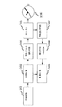
図1は、本発明の実施の形態に係るモータ制御回路を用いたアナログ電子時計のブロック図で、アナログ電子腕時計の例を示している。
図1において、アナログ電子時計は、所定周波数の信号を発生する発振回路101、発振回路101で発生した信号を分周して計時の基準となる時計信号を発生する分周回路102、電子時計を構成する各電子回路要素の制御や駆動パルスの変更制御等の制御を行う制御回路103、制御回路103からの制御信号に基づいてモータ回転駆動用の駆動パルスを選択し出力する駆動パルス選択回路104、駆動パルス選択回路104からの駆動パルスによって回転駆動されるステッピングモータ105、ステッピングモータ105によって回転駆動され時刻を表示するための時刻針を有するアナログ表示部106を備えている。
FIG. 1 is a block diagram of an analog electronic timepiece using a motor control circuit according to an embodiment of the present invention, and shows an example of an analog electronic wristwatch.
In FIG. 1, an analog electronic timepiece includes an
また、アナログ電子時計は、ステッピングモータ105の回転状況を表す誘起信号を所定の検出区間において検出する回転検出回路107、回転検出回路107が所定の基準しきい電圧Vcompを超える誘起信号VRsを検出した時刻と検出した区間とを比較して、前記誘起信号VRsがどの区間において検出されたのかを判定する検出区間判別回路108を有している。後述するように、ステッピングモータ105が回転したか否かを検出する検出区間は3つの区間に区分している。
Further, in the analog electronic timepiece, the
回転検出回路107は、前記特許文献1に記載された回転検出回路と同様の原理を利用して誘起信号を検出する構成のものであり、所定の基準しきい電圧Vcompを越える誘起信号VRsを検出する。
ここで、発振回路101及び分周回路102は信号発生手段を構成し、アナログ表示部106は時刻表示手段を構成している。回転検出回路107は回転検出手段を構成し、制御回路103、駆動パルス選択回路104及び検出区間判別回路108は制御手段を構成している。
The
Here, the
図2は、本発明の実施の形態に使用するステッピングモータ105の構成図で、アナログ電子時計で一般に用いられている時計用ステッピングモータの例を示している。
図2において、ステッピングモータ105は、ロータ収容用貫通孔203を有するステータ201、ロータ収容用貫通孔203に回転可能に配設されたロータ202、ステータ201と接合された磁心208、磁心208に巻回されたコイル209を備えている。ステッピングモータ105をアナログ電子時計に用いる場合には、ステータ201及び磁心208はネジ(図示せず)によって地板(図示せず)に固定され、互いに接合される。コイル201は、第1端子OUT1、第2端子OUT2を有している。
FIG. 2 is a configuration diagram of the
In FIG. 2, the
ロータ202は、2極(S極及びN極)に着磁されている。磁性材料によって形成されたステータ201の外端部には、ロータ収容用貫通孔203を挟んで対向する位置に複数(本実施の形態では2個)の切り欠き部(外ノッチ)206、207が設けられている。各外ノッチ206、207とロータ収容用貫通孔203間には可飽和部210、211が設けられている。
The
可飽和部210、211は、ロータ202の磁束によっては磁気飽和せず、コイル209が励磁されたときに磁気飽和して磁気抵抗が大きくなるように構成されている。ロータ収容用貫通孔203は、輪郭が円形の貫通孔の対向部分に複数(本実施の形態では2つ)の半月状の切り欠き部(内ノッチ)204、205を一体形成した円孔形状に構成されている。
The
切り欠き部204、205は、ロータ202の停止位置を決めるための位置決め部を構成している。コイル209が励磁されていない状態では、ロータ202は、図2に示すように前記位置決め部に対応する位置、換言すれば、ロータ202の磁極軸Aが、切り欠き部204、205を結ぶ線分と直交するような位置(角度θ0位置)に安定して停止している。ロータ202の回転軸(回転中心)を中心とするXY座標空間を4つの象限(第1象限I〜第4象限IV)に区分している。
The
いま、駆動パルス選択回路104から矩形波の駆動パルスをコイル209の端子OUT1、OUT2間に供給して(例えば、第1端子OUT1側を正極、第2端子OUT2側を負極)、図2の矢印方向に電流iを流すと、ステータ201には破線矢印方向に磁束が発生する。これにより、可飽和部210、211が飽和して磁気抵抗が大きくなり、その後、ステータ201に生じた磁極とロータ202の磁極との相互作用によって、ロータ202は図2の矢印方向に180度回転し、磁極軸が角度θ1位置で安定的に停止する。尚、ステッピングモータ105を回転駆動することによって通常動作(本実施の形態ではアナログ電子時計であるため運針動作)を行わせるための回転方向(図2では反時計回り方向)を正方向とし、その逆(時計回り方向)を逆方向としている。
Now, a rectangular-wave drive pulse is supplied from the drive
次に、駆動パルス選択回路104から、逆極性の矩形波の駆動パルスをコイル209の端子OUT1、OUT2に供給して(前記駆動とは逆極性となるように、第1端子OUT1側を負極、第2端子OUT2側を正極)、図2の反矢印方向に電流を流すと、ステータ201には反破線矢印方向に磁束が発生する。これにより、可飽和部210、211が先ず飽和し、その後、ステータ201に生じた磁極とロータ202の磁極との相互作用によって、ロータ202は前記と同一方向(正方向)に180度回転し、磁極軸が角度θ0位置で安定的に停止する。
Next, from the drive
以後このように、コイル209に対して極性の異なる信号(交番信号)を供給することによって、前記動作が繰り返し行われて、ロータ202を180度ずつ矢印方向に連続的に回転させることができるように構成されている。尚、本実施の形態では、駆動パルスとして、後述するように、相互にエネルギの異なる複数の主駆動パルスP11〜P1n及び補正駆動パルスP2を用いている。
Thereafter, by supplying signals having different polarities (alternating signals) to the
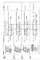
図3は、本実施の形態において、主駆動パルスP1によってステッピングモータ105を駆動した場合のタイミング図で、負荷の状態、ロータ202の回転挙動及びパルス制御動作をあわせて示している。
図3において、P1は主駆動パルスP1を表すと共にロータ202が主駆動パルスP1によって回転駆動される区間を表し、領域a〜eは主駆動パルスP1の駆動停止後の自由振動によってロータ202が回転する位置を表す領域である。
FIG. 3 is a timing chart when the stepping
In FIG. 3, P1 represents a main drive pulse P1 and a section in which the
主駆動パルスP1による駆動直後の所定の検出区間を第1区間T1、第1区間T1よりも後の所定時間を第2区間T2、第2区間よりも後の所定時間を第3区間T3としている。このように、主駆動パルスP1による駆動終了直後から始まる検出区間T全体を複数の区間(本実施の形態では3つの区間T1〜T3)に区分している。尚、本実施の形態では、誘起信号VRsを検出しない期間であるマスク区間は設けていない。
ロータ202を中心として、その回転によってロータ202の主磁極が位置するXY座標空間を第1象限I〜第4象限IVに区分した場合、第1区間T1〜第3区間T3は次のように表すことができる。
A predetermined detection period immediately after driving by the main drive pulse P1 is a first period T1, a predetermined time after the first period T1 is a second period T2, and a predetermined time after the second period is a third period T3. . In this way, the entire detection section T starting immediately after the end of driving by the main drive pulse P1 is divided into a plurality of sections (three sections T1 to T3 in the present embodiment). In the present embodiment, there is no mask section that is a period during which no induced signal VRs is detected.
When the XY coordinate space in which the main magnetic pole of the
即ち、通常負荷の状態において、第1区間T1はロータ202を中心とする空間の第3象限IIIにおいてロータ202の正方向回転状況を判定する区間及び最初の逆方向回転状況を判定する区間、第2区間T2は第3象限IIIにおいてロータ202の最初の逆方向回転状況を判定する区間、第3区間T3は第3象限IIIにおいてロータ202の最初の逆方向回転後の回転状況を判定する区間である。ここで、通常負荷とは通常時に駆動される負荷を意味しており、本実施の形態では、時刻針を駆動する場合の負荷を通常負荷としている。
That is, in the normal load state, the first section T1 includes a section for determining the forward rotation state of the
Vcompはステッピングモータ105で発生する誘起信号VRsの電圧レベルを判定する基準しきい電圧であり、ステッピングモータ105が回転した場合等のようにロータ202が一定の速い動作を行った場合には誘起信号VRsが基準しきい電圧Vcompを超え、回転しない場合等のようにロータ202が一定の速い動作を行わない場合には誘起信号VRsが基準しきい電圧Vcompを超えないように基準しきい電圧Vcompは設定されている。
例えば、図3において、本実施の形態に係るステッピングモータ制御回路では、通常負荷の状態において、領域bで生じた誘起信号VRsは第1区間T1において検出され、領域cで生じた誘起信号VRsは第1区間T1及び第2区間T2において検出され、領域cの後に生じた誘起信号VRsは第3区間T3において検出される。
Vcomp is a reference threshold voltage for determining the voltage level of the induced signal VRs generated by the stepping
For example, in FIG. 3, in the stepping motor control circuit according to the present embodiment, in the normal load state, the induced signal VRs generated in the region b is detected in the first section T1, and the induced signal VRs generated in the region c is The induced signal VRs detected after the first interval T1 and the second interval T2 and generated after the region c is detected during the third interval T3.
回転検出回路107が基準しきい電圧Vcompを超える誘起信号VRsを検出した場合をその区間の判定値「1」、回転検出回路107が基準しきい電圧Vcompを超える誘起信号VRsを検出できなかった場合をその区間の判定値「0」とすると、駆動負荷の状態が図3の通常負荷の例では、回転状況を表す誘起信号VRsのパターン(第1区間T1の判定値,第2区間T2の判定値,第3区間T3の判定値)として(0,1,0)が得られており、制御回路103は駆動エネルギが過大(余裕回転)と判定して、主駆動パルスP1の駆動エネルギを1ランクダウン(パルスダウン)するようにパルス制御を行う。
When the
また、負荷増分小の状態においては、領域aで生じた誘起信号VRsは第1区間T1において検出され、領域bで生じた誘起信号は第1区間T1及び第2区間T2において検出され、領域cで生じた誘起信号は第2区間T2及び第3区間T3において検出される。図3では、パターン(1,1,0)が得られており、制御回路103は駆動エネルギが適切(余裕ない回転)と判定して、主駆動パルスP1の駆動エネルギを変更せずに維持するようにパルス制御を行う。
In a state where the load increment is small, the induced signal VRs generated in the region a is detected in the first interval T1, the induced signal generated in the region b is detected in the first interval T1 and the second interval T2, and the region c The induced signal generated in is detected in the second interval T2 and the third interval T3. In FIG. 3, the pattern (1, 1, 0) is obtained, and the
図6は負荷状況に応じた前記動作をまとめた判定チャートである。図6において、前述したとおり、基準しきい電圧Vcompを超える誘起信号VRsを検出した場合をその区間の判定値「1」、基準しきい電圧Vcompを超える誘起信号VRsを検出できなかった場合をその区間の判定値「0」と表している。また、「0/1」や「1/0」は、その区間の判定値が「1」、「0」のどちらでもよいことを表している。判定チャートは制御回路103内の記憶手段(図示せず)に予め記憶されている。
FIG. 6 is a determination chart summarizing the operations according to the load status. In FIG. 6, as described above, when the induced signal VRs exceeding the reference threshold voltage Vcomp is detected, the determination value “1” in that section, and when the induced signal VRs exceeding the reference threshold voltage Vcomp cannot be detected The judgment value “0” for the section is shown. Further, “0/1” and “1/0” indicate that the determination value of the section may be “1” or “0”. The determination chart is stored in advance in storage means (not shown) in the
図6に示すように、回転検出回路107が基準しきい電圧Vcompを超える誘起信号VRsの有無を検出し、検出区間判別回路108が前記誘起信号VRsの検出時期を判定したパターンに基づいて、制御回路103は自己の内部に記憶した図6の判定チャートを参照して、制御回路103及び駆動パルス選択回路104は主駆動パルスP1のパルスアップやパルスダウンあるいは補正駆動パルスP2による駆動等の後述する駆動パルス制御を行ってステッピングモータ105を回転制御する。
As shown in FIG. 6, the
例えば、制御回路103は、パターン(1/0,0,0)の場合、ステッピングモータ105が回転していない(非回転)と判定して、補正駆動パルスP2によってステッピングモータ105を駆動するように駆動パルス選択回路104を制御した後、次回駆動時に1ランクアップした主駆動パルスP1に変更して駆動するように駆動パルス選択回路104を制御する。
For example, in the case of the pattern (1/0, 0, 0), the
制御回路103は、パターン(1/0,0,1)の場合、ステッピングモータ105は回転したが、通常負荷に対して大きい負荷が増えた状態(負荷増分大)であり、次回駆動時に非回転になる恐れがある(ぎりぎり回転)と判定して、非回転になることを予防するために補正駆動パルスP2による駆動を行うことなく、早めに次回駆動時に1ランクアップした主駆動パルスP1に変更して駆動するように駆動パルス選択回路104を制御する。
In the case of the pattern (1/0, 0, 1), the
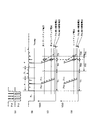
図4は、本実施の形態においてパターン(1,0,1)が発生して主駆動パルスP1をランクアップする場合の動作説明図で、基準しきい電圧Vcompを超える誘起信号VRsが検出される時と駆動電圧との関係を併せて示している。
同図(A)は、駆動エネルギランクが第1ランクの主駆動パルスP11、第4ランクの主駆動パルスP14(P11<P14)を示す波形図で、主駆動パルスとしてパルス幅が一定の櫛歯状の主駆動パルスを用いてデューティ比を変えることによって駆動エネルギのランクを変えるように構成している。主駆動パルスとして矩形波状の主駆動パルスを使用してもよく、この場合は、パルス幅を変えることによって駆動エネルギのランクを変えることになる。
FIG. 4 is an operation explanatory diagram when the pattern (1, 0, 1) is generated and the main drive pulse P1 is ranked up in the present embodiment, and the induced signal VRs exceeding the reference threshold voltage Vcomp is detected. The relationship between time and drive voltage is also shown.
FIG. 5A is a waveform diagram showing a main drive pulse P11 having a drive energy rank of 1st rank and a main drive pulse P14 having a 4th rank (P11 <P14), and comb teeth having a constant pulse width as the main drive pulse. The rank of the drive energy is changed by changing the duty ratio using the main drive pulse in the form of a ring. A rectangular main drive pulse may be used as the main drive pulse. In this case, the rank of the drive energy is changed by changing the pulse width.
同図(B)は、主駆動パルスP1によって駆動した場合に発生する誘起信号VRsと基準しきい電圧Vcompとの関係を示す図である。図の例では、領域a、cにおいて、基準しきい電圧Vcompを超える誘起信号VRsが検出されており、以下の同図(C)、(D)において誘起信号VRsの判定値パターン(1,0,1)が得られるように区間が設定される。 FIG. 5B is a diagram showing the relationship between the induced signal VRs generated when driven by the main drive pulse P1 and the reference threshold voltage Vcomp. In the example shown in the figure, the induced signal VRs exceeding the reference threshold voltage Vcomp is detected in the regions a and c, and the judgment value pattern (1, 0) of the induced signal VRs is shown in (C) and (D) below. , 1) is set to obtain a section.
同図(C)は、第2区間T2を所定時間に固定した場合に、基準しきい電圧Vcompを超える誘起信号VRsが検出される時点tと駆動電圧との関係を示す図で、ランクアップ電圧が主駆動パルスの駆動エネルギの大きさによって変化する様子を示している。ここで、ランクアップ電圧とは、補正駆動パルスP2による駆動を行うことなく主駆動パルスP1をランクアップしてステッピングモータ105を駆動するときの駆動電圧であり、具体的には、パターン(0/1,0,1)が発生して主駆動パルスをランクアップして駆動するときの駆動電圧である。
FIG. 10C is a diagram showing the relationship between the driving time and the time t when the induced signal VRs exceeding the reference threshold voltage Vcomp is detected when the second section T2 is fixed at a predetermined time. Shows a state that changes depending on the drive energy of the main drive pulse. Here, the rank-up voltage is a drive voltage when the stepping
破線は主駆動パルスP11によって駆動した際に基準しきい電圧Vcompを超える誘起信号VRsが発生する時点tと駆動電圧との関係を示し、又、実線は主駆動パルスP14によって駆動した際に基準しきい電圧Vcompを超える誘起信号VRsが発生する時点tと駆動電圧との関係を示している。尚、P11最小駆動電圧、P14最小駆動電圧は、各々、主駆動パルスP11、P14によってステッピングモータ105を回転させることが可能な最小の駆動電圧である。
The broken line indicates the relationship between the drive time and the time t when the induced signal VRs exceeding the reference threshold voltage Vcomp is generated when driven by the main drive pulse P11, and the solid line is referenced when driven by the main drive pulse P14. The relationship between the drive time and the time t when the induced signal VRs exceeding the threshold voltage Vcomp is generated is shown. The P11 minimum drive voltage and the P14 minimum drive voltage are minimum drive voltages that can rotate the stepping
主駆動パルスP11、P14のいずれで駆動した場合も、駆動電圧が低下するにしたがってステッピングモータ105の回転が遅くなるため基準しきい電圧Vcompを超える誘起信号VRsの発生時期が遅くなるが、主駆動パルスによる駆動からの経過時間が長い程それが顕著になっている。例えば第3区間T3では第1区間T1に比べて、主駆動パルスP11による駆動の場合の方が主駆動パルスP14による駆動の場合よりもより遅く発生している。
When driven by either of the main drive pulses P11 and P14, the rotation of the stepping
主駆動パルスP11、P14のいずれで駆動した場合も、第1区間T1において判定値「1」、第2区間T2おいて判定値「0」、第3区間T3において判定値「1」が得られている。第2区間の長さが一定値に固定されており、主駆動パルスP11、P14のいずれで駆動した場合も、○印で示すように第3区間T3に入った同じ時点で判定値「1」が検出され、制御回路103はこの時点でパターン(1,0,1)が発生したと判定することになる。したがって、図示するように、主駆動パルスP11駆動時のランクアップ電圧は主駆動パルスP14駆動時のランクアップ電圧よりも大きい値となる。
When driven by either of the main drive pulses P11 and P14, the determination value “1” is obtained in the first interval T1, the determination value “0” is obtained in the second interval T2, and the determination value “1” is obtained in the third interval T3. ing. The length of the second section is fixed to a constant value, and when it is driven by either of the main drive pulses P11 and P14, the judgment value “1” is entered at the same time when the third section T3 is entered as indicated by a circle. Is detected, and the
このように、主駆動パルスのエネルギ量が小さくなるほどロータ202の回転速度が落ちて、第3象限IIIの誘起信号VRsの発生タイミングが遅くなる。このため、エネルギ量が高い駆動パルスP14のランクアップ駆動余裕にあわせて最適化して第3区間T3を設定すると、エネルギ量が低い駆動パルスP11の場合、最小駆動電圧に対して必要以上に高い電圧でランクアップを行ってしまい、低消費化に限界を生じる。
Thus, as the energy amount of the main drive pulse decreases, the rotational speed of the
同図(D)は本実施の形態における動作を説明する図であり、同図(C)の問題を解消するようにしている。
即ち、本実施の形態では、同図(D)に示すように、制御回路103は、主駆動パルスP1の駆動エネルギ(櫛歯状主駆動パルスの場合はデューティ比、矩形波状主駆動パルスの場合はパルス幅)に応じて第2区間T2の長さを変えるように制御する。同図(D)の例では、制御回路103は主駆動パルスP1の駆動エネルギが小さい(駆動エネルギのランクが低い)ほど、第2区間T2が長くなるように設定する。また、制御回路103は各主駆動パルスP1のランクアップ電圧の差が所定範囲内になるように、好ましくは等しくなるように第2区間T2を変えるようにしている。また、制御回路103は検出区間T全体の長さが変化しないように、第2区間T2の変化量に応じて第3区間T3を短くしている。
FIG. 4D is a diagram for explaining the operation in the present embodiment, and solves the problem shown in FIG.
That is, in this embodiment, as shown in FIG. 4D, the
換言すれば、制御回路103は、予め定めた主駆動パルスP1毎に定めたエネルギ(具体的には駆動エネルギのランク)に応じて第3区間T3の開始タイミングを変えるように制御する。同図(D)の例では、制御回路103は予め定めた主駆動パルスP1のエネルギが小さい(駆動エネルギのランクが低い)ほど、第3区間T3の開始タイミングが遅くなるように設定する。また、制御回路103は各主駆動パルスP1のランクアップ電圧の差が所定範囲内になるように、好ましくは等しくなるように第3区間T3の開始タイミングを変えるようにしている。また、制御回路103は検出区間T全体の長さが変化しないように、第3区間T3の開始タイミングの変化量に応じて第2区間T2の長さを変化させている。
In other words, the
同図(D)において、主駆動パルスP11では第1区間をT1、第2区間をT21、第3区間をT31とし、主駆動パルスP14では第1区間を主駆動パルスP11と同じT1、第2区間をT21より短いT24、第3区間をT31より長いT34としている。尚、各主駆動パルスにおける検出区間T全体は同一になるように構成する場合には、主駆動パルスP11の第2区間T21と第3区間T31の和は、主駆動パルスP14の第2区間T24と第3区間T34の和に等しくなるように設定する。 In FIG. 4D, in the main drive pulse P11, the first interval is T1, the second interval is T21, and the third interval is T31. In the main drive pulse P14, the first interval is the same as the main drive pulse P11. The section is T24 shorter than T21, and the third section is T34 longer than T31. When the entire detection interval T in each main drive pulse is configured to be the same, the sum of the second interval T21 and the third interval T31 of the main drive pulse P11 is the second interval T24 of the main drive pulse P14. And the third section T34.
制御回路103は、各主駆動パルスP1と第2区間T2の長さを対応付けた区間テーブルをその記憶手段に予め記憶しており、回転検出時に前記区間テーブルを参照して、現在の主駆動パルスP1に対応する長さの第2区間T2を選定する。第2区間の長さとともに第3区間の長さも併せて前記区間テーブルに格納しておいて、第1区間は一定とし、第2区間とともに第3区間を変えるようにしてもよい。検出区間判別回路108は、制御回路103によって設定された長さの各第1区間〜第3区間を用いて、前記各区間において回転検出回路107が検出した誘起信号VRsの判定値を得る。
The
同図(D)では、主駆動パルスP11で駆動した場合、第1区間T1において判定値「1」、第2区間T21おいて判定値「0」、○印で示すように第3区間T31において判定値「1」が得られている。また、主駆動パルスP14で駆動した場合、第1区間T1において判定値「1」、第2区間T24おいて判定値「0」、○印で示すように第3区間T34において判定値「1」が得られている。制御回路103は、主駆動パルスP11、P14のいずれの場合も、前記○印の時点でパターン(1,0,1)が発生したと判定する。この場合のランクアップ電圧は同一になっており、前記ランクアップ電圧は各主駆動パルスの最小駆動電圧よりも高くなるように設定されている。
In FIG. 4D, when driven by the main drive pulse P11, the determination value “1” in the first interval T1, the determination value “0” in the second interval T21, and in the third interval T31 as indicated by a circle. The judgment value “1” is obtained. Further, when driven by the main drive pulse P14, the determination value “1” in the first section T1, the determination value “0” in the second section T24, and the determination value “1” in the third section T34 as indicated by a circle. Is obtained. The
このように、第2区間T2を各主駆動パルスのエネルギに応じた長さT2nに変えることによってランクアップ電圧を低い値に設定することにより、各主駆動パルス毎のランクアップ電圧を下げて消費電力を低減することが可能になる。また、駆動余力を適切に判定することによって主駆動パルスのランク変更動作を最適化し低消費化を図ることが可能になる。
図5は、本発明の実施の形態に係るステッピングモータ制御回路及びアナログ電子時計の動作を示すフローチャートであり、主として制御回路103の処理を示すフローチャートである。
以下、図1〜図6を参照して、本発明の実施の形態に係るステッピングモータ制御回路及びアナログ電子時計の動作を詳細に説明する。
In this way, the rank-up voltage is set to a low value by changing the second section T2 to the length T2n corresponding to the energy of each main drive pulse, thereby reducing the rank-up voltage for each main drive pulse and consuming it. It becomes possible to reduce electric power. In addition, it is possible to optimize the rank change operation of the main drive pulse and to reduce the consumption by appropriately determining the drive capacity.
FIG. 5 is a flowchart showing operations of the stepping motor control circuit and the analog electronic timepiece according to the embodiment of the present invention, and is a flowchart mainly showing processing of the
Hereinafter, the operations of the stepping motor control circuit and the analog electronic timepiece according to the embodiment of the present invention will be described in detail with reference to FIGS.
図1において、発振回路101は所定周波数の基準クロック信号を発生し、分周回路102は発振回路101で発生した前記信号を分周して計時の基準となる時計信号を発生し、制御回路103に出力する。
制御回路103は、前記時間信号を計数して計時動作を行い、先ず主駆動パルスP1nのランク1にして(図5のステップS501)、最小駆動エネルギの主駆動パルスP11でステッピングモータ105を回転駆動するように制御信号を出力する(ステップS502、S503)。
In FIG. 1, an
The
駆動パルス選択回路104は、制御回路103からの制御信号に応答して、主駆動パルスP11によってステッピングモータ105を回転駆動する。ステッピングモータ105は主駆動パルスP11によって回転駆動されて、アナログ表示部106を駆動する。これにより、ステッピングモータ105が正常に回転した場合には、アナログ表示部106では、時刻針によって現在時刻が随時表示される。
制御回路103は、ステッピングモータ105を回転駆動後、自己が予め記憶している前記区間テーブルを参照して第1区間〜第3区間を、主駆動パルスP1のランクに応じた長さの区間に設定して、ステッピングモータ105の回転状況の判定を行う。
In response to the control signal from the
After rotating the stepping
制御回路103は、回転検出回路107が所定の基準しきい電圧Vcompを超えるステッピングモータ105の誘起信号VRsを検出したか否かの判定、及び、検出区間判別回路108が前記誘起信号VRsの検出時刻tは第1区間T1内と判定したか否かの判定(即ち、基準しきい電圧Vcompを超える誘起信号VRsを第1区間T1内で検出したか否かの判定)を行って(ステップS504)、基準しきい電圧Vcompを超える誘起信号VRsを第1区間T1内で検出していないと判定した場合には、前記同様にして、基準しきい電圧Vcompを超える誘起信号VRsを第2区間T2n内で検出したか否かを判定する(ステップS505)。
制御回路103は、処理ステップS505において、基準しきい電圧Vcompを超える誘起信号VRsを第2区間T2n内で検出していないと判定した場合、前記同様にして、基準しきい電圧Vcompを超える誘起信号VRsを第3区間T3n内で検出したか否かを判定する(ステップS506)。
The
When determining that the induced signal VRs exceeding the reference threshold voltage Vcomp is not detected in the second section T2n in the processing step S505, the
制御回路103は、処理ステップS506において、基準しきい電圧Vcompを超える誘起信号VRsを第3区間T3n内で検出していないと判定した場合、補正駆動パルスP2によってステッピングモータ105を駆動した後(ステップS507)、当該主駆動パルスP1のランクnが最大ランクmでない場合には主駆動パルスP1を1ランクアップして主駆動パルスP1(n+1)に変更した後に処理ステップS502に戻り、次回の駆動はこの主駆動パルスP1(n+1)によって駆動する(ステップS508、S509;図3及び図6の非回転の場合である。)。
When determining that the induced signal VRs exceeding the reference threshold voltage Vcomp is not detected in the third section T3n in the processing step S506, the
制御回路103は、処理ステップS508において、当該主駆動パルスP1のランクnが最大ランクmの場合には、主駆動パルスP1を変更せずに処理ステップS502に戻る(ステップS514)。
制御回路103は、処理ステップS506において、基準しきい電圧Vcompを超える誘起信号VRsを第3区間T3内で検出したと判定した場合(図4(D)に示したような判定値パターンが(0/1,0,1)の場合であり、図3及び図6の負荷増分大の場合である。)、当該主駆動パルスP1のランクnが最大ランクmでない場合には、主駆動パルスP1を1ランクアップして主駆動パルスP1(n+1)に変更して処理ステップS502に戻り、次回の駆動はこの主駆動パルスP1によって駆動する(ステップS510、S509)。
If the rank n of the main drive pulse P1 is the maximum rank m in process step S508, the
When the
このように、主駆動パルスのエネルギ量にかかわらず一律、同一検出区間でステッピングモータ105の回転状況を判定するのではなく(図4(C)参照)、主駆動パルスのエネルギ量に応じて、区間の長さを変化させることにより、全ての主駆動パルスのランクでのランクアップ駆動余裕度を最適化して、低消費化を図ることができる。即ち、駆動余力を適切に判定することによって主駆動パルスのランク変更動作を最適化し低消費化を図ることが可能になる。
Thus, instead of determining the rotation state of the stepping
制御回路103は、処理ステップS510において、当該主駆動パルスP1のランクnが最大ランクmの場合にはランク変更できないため、主駆動パルスP1は変更せずに維持して処理ステップS502に戻り、次回の駆動はこの主駆動パルスP1によって駆動する(ステップS511)。
制御回路103は、処理ステップS504において、基準しきい電圧Vcompを超える誘起信号VRsを第1区間T1内で検出したと判定した場合、前記同様にして、基準しきい電圧Vcompを超える誘起信号VRsを第2区間T2n内で検出したか否かを判定する(ステップS512)。
Since the rank cannot be changed when the rank n of the main drive pulse P1 is the maximum rank m in the process step S510, the
When determining that the induced signal VRs exceeding the reference threshold voltage Vcomp is detected within the first section T1 in the processing step S504, the
制御回路103は、処理ステップS512において、基準しきい電圧Vcompを超える誘起信号VRsを第2区間T2n内で検出していないと判定した場合、処理ステップS506に移行して前記処理を行う。
制御回路103は、処理ステップS512において、基準しきい電圧Vcompを超える誘起信号VRsを第2区間T2内で検出したと判定した場合、処理ステップS511に移行する(図3及び図6の負荷増分小の場合である。)。
If the
When the
一方、制御回路103は、処理ステップS505において、基準しきい電圧Vcompを超える誘起信号VRsを区間T2n内で検出したと判定した場合(図3及び図6の通常負荷の場合である。)、主駆動パルスP1のランクnが最低ランク1のときはランクを下げることができないためランクを変更せずに処理ステップS502に戻り(ステップS513、S514)、主駆動パルスP1のランクnが最低ランク1でないときは主駆動パルスP1を1ランクダウンして処理ステップS502に戻る(ステップS513、S515)。これにより、駆動余力が更に大きいときは主駆動パルスP1を直ちにパルスダウンして、安定駆動を維持すると共に省電力化を図ることができる。
On the other hand, when the
図7は本発明の他の実施の形態の動作説明図、図8は本発明の他の実施のフローチャートで、各々、前記実施の形態の図4、図5に対応する図であり、同一部分には同一符号を付している。
前記実施の形態では、主駆動パルスP1のランクに応じて1つの区間の開始タイミングを遅くするように構成したが、本他の実施の形態では主駆動パルスP1のランクに応じて複数の区間のタイミングを遅くするように構成している。
以下、本他の実施の形態の動作を、前記実施の形態と相違する部分について説明する。
FIG. 7 is a diagram for explaining the operation of another embodiment of the present invention, and FIG. 8 is a flowchart of another embodiment of the present invention, corresponding to FIGS. 4 and 5 of the above-described embodiment. Are denoted by the same reference numerals.
In the above-described embodiment, the start timing of one section is delayed according to the rank of the main drive pulse P1, but in this other embodiment, a plurality of sections according to the rank of the main drive pulse P1. It is configured to delay the timing.
In the following, the operation of the other embodiment will be described with respect to parts different from the above embodiment.
尚、本他の実施の形態のブロック図やパルス制御動作は前記実施の形態と同一であるが、本他の実施の形態においては、制御回路103は、各主駆動パルスP1毎に第2区間T2及び第3区間T3の開始タイミングを対応付けた区間テーブルをその記憶手段に予め記憶しており、回転検出時に前記区間テーブルを参照して、第2区間T2及び第3区間T3の開始タイミングを予め定めた主駆動パルスP1のエネルギランクに応じたタイミングに設定する。この場合も、検出区間Tの長さは一定になるように構成している。
The block diagram and the pulse control operation of the other embodiment are the same as those of the above embodiment, but in the other embodiment, the
例えば、図7(D)の例では、主駆動パルスP11に対応して設定される検出区間Tは第1区間T11、第2区間T21、第3区間T31に区分され、主駆動パルスP14に対応して設定される検出区間Tは第1区間T14、第2区間T24、第3区間T34に区分される。また、第2区間T21の開始タイミングは第2区間T24の開始タイミングよりも遅くなるように設定され又、第3区間T31の開始タイミングは第3区間T34の開始タイミングよりも遅くなるように設定されている。主駆動パルスP1のエネルギに応じて検出区間Tを区分した状態で回転状況の判定が行われる。
また、図4では、主駆動パルスP11、P14によってステッピングモータ105を回転させることが可能な最小の駆動電圧であるP11最小駆動電圧、P14最小駆動電圧は図示せずに省略したが、図7にはP11最小駆動電圧、P14最小駆動電圧を明記している。
For example, in the example of FIG. 7D, the detection interval T set corresponding to the main drive pulse P11 is divided into a first interval T11, a second interval T21, and a third interval T31, and corresponds to the main drive pulse P14. The detection section T thus set is divided into a first section T14, a second section T24, and a third section T34. The start timing of the second section T21 is set to be later than the start timing of the second section T24, and the start timing of the third section T31 is set to be later than the start timing of the third section T34. ing. The rotation state is determined in a state where the detection section T is divided according to the energy of the main drive pulse P1.
In FIG. 4, the P11 minimum drive voltage and the P14 minimum drive voltage, which are the minimum drive voltages that can rotate the stepping
図1において、制御回路103は、分周回路102からの時間信号を計数して計時動作を行い、主駆動パルスP1nのランク1にして、最小駆動エネルギの主駆動パルスP11でステッピングモータ105を回転駆動するように制御信号を出力する(図8のステップS501〜S503)。
駆動パルス選択回路104は、制御回路103からの制御信号に応答して、主駆動パルスP11によってステッピングモータ105を回転駆動する。ステッピングモータ105は主駆動パルスP11によって回転駆動されて、アナログ表示部106を駆動する。これにより、ステッピングモータ105が正常に回転した場合には、アナログ表示部106では、時刻針によって現在時刻が随時表示される。
In FIG. 1, the
In response to the control signal from the
制御回路103は、ステッピングモータ105を回転駆動後、自己が予め記憶している区間テーブルを参照して第2区間及び第3区間の開始タイミングを、主駆動パルスP1のランクに応じて設定し、ステッピングモータ105の回転状況の判定を行う。即ち、制御回路103は、前記区間テーブルを参照して、主駆動パルスP1のランクが小さいほど、第2区間及び第3区間の開始タイミングが遅くなるように設定し、ステッピングモータ105の回転状況の判定を行う。
The
制御回路103は、回転検出回路107が所定の基準しきい電圧Vcompを超えるステッピングモータ105の誘起信号VRsを検出したか否かの判定、及び、検出区間判別回路108が前記誘起信号VRsの検出時刻tは第1区間T1n(ここでは、n=1のため第1区間T11)内と判定したか否かの判定(即ち、基準しきい電圧Vcompを超える誘起信号VRsを第1区間T1n内で検出したか否かの判定)を行って(ステップS801)、基準しきい電圧Vcompを超える誘起信号VRsを第1区間T1n内で検出していないと判定した場合には、前記同様にして処理ステップS505以降の処理を行う。
The
また、制御回路103は、処理ステップS801において基準しきい電圧Vcompを超える誘起信号VRsを第1区間T1n内で検出したと判定した場合、前記同様にして、処理ステップS512以降の処理を行う。
本他の実施の形態においては、主駆動パルスP1のエネルギが小さいほど、第2区間T2及び第3区間T3の開始タイミングを遅くして回転状況を判定するようにしているため、駆動余力を適切に判定することが可能になり、主駆動パルスP1のランク変更動作を最適化し低消費化を図ることが可能になる。また、ランクアップ駆動余裕度を最適化して、低消費化を図ることが可能になるという効果を奏する。
If the
In the other embodiments, as the energy of the main drive pulse P1 is smaller, the start timing of the second section T2 and the third section T3 is delayed to determine the rotation state. Thus, it is possible to optimize the rank changing operation of the main drive pulse P1 and reduce the consumption. In addition, it is possible to optimize the rank-up drive margin and reduce the consumption.
図9は本発明の更に他の実施の形態に係るモータ制御回路を用いたアナログ電子時計のブロック図、図10は本他の実施の形態の動作説明図、図11は本他の実施の形態のフローチャートで、各々、前記実施の形態の図1、図4、図5に対応する図であり、同一部分には同一符号を付している。
図9において、本他の実施の形態では、ステッピングモータ105やステッピングモータ制御回路をはじめとするアナログ電子時計の電子的構成要素を駆動する電源として電池902を有しており、又、電池902の電圧を検出する電源電圧検出回路901を備えている。ここで、電源電圧検出回路901は電源電圧検出手段を構成している。また、制御回路103、駆動パルス選択回路104、検出区間判別回路108及び電源電圧検出回路901は制御手段を構成している。
9 is a block diagram of an analog electronic timepiece using a motor control circuit according to still another embodiment of the present invention, FIG. 10 is an operation explanatory diagram of the other embodiment, and FIG. 11 is another embodiment of the present invention. These flowcharts correspond to FIGS. 1, 4, and 5, respectively, and the same parts are denoted by the same reference numerals.
In FIG. 9, in another embodiment, a battery 902 is provided as a power source for driving electronic components of an analog electronic timepiece including the stepping
本他の実施の形態においては、制御回路103は、各ランクの主駆動パルスP1及び所定電源電圧と第2区間T2及び第3区間T3の開始タイミングとを対応付けた区間テーブルをその記憶手段に予め記憶しており、回転検出時に前記区間テーブルを参照して、第2区間T2及び第3区間T3の開始タイミングを、予め定めた主駆動パルスP1のエネルギランク及び電源電圧検出回路901が検出した電池902の電圧に応じたタイミングに設定する。このように、本他の実施の形態では、主駆動パルスP1のエネルギランク及び電源の電圧値に応じて複数の区間の開始タイミングを変えるように構成している。この場合も、検出区間Tの長さは一定になるように構成している。
In this other embodiment, the
以下、本他の実施の形態の動作を、前記各実施の形態と相違する部分について詳細に説明する。
図11において、制御回路103は、分周回路102からの時間信号を計数して計時動作を行い、主駆動パルスP1nのランク1に設定し(ステップS501)、電源電圧検出回路901が検出した電池902の電圧Vddの大きさを判定する(ステップS111、S113)。
Hereinafter, the operation of the other embodiments will be described in detail with respect to portions different from the respective embodiments.
In FIG. 11, the
制御回路103は、電池902の電圧Vddが所定の第1ランクアップ電圧(第1電圧)V1を超える場合にはランクアップ電圧種別iを1(即ちランクアップ電圧V1)に設定する(ステップS112;図10(D)参照)。制御回路103は、自己が予め記憶している区間テーブルを参照して、主駆動パルスP1のランク及びランクアップ電圧種別iに応じて第2区間及び第3区間の開始タイミングを設定する。ここでも検出区間Tの長さは一定となるようにする。
When the voltage Vdd of the battery 902 exceeds a predetermined first rank-up voltage (first voltage) V1, the
この場合、主駆動パルスP1のランクnが1でランクアップ電圧種別iが1のため、図10(D)に示すように、検出区間Tは第1区間T111、第2区間T211、第3区間T311に区分される。尚、主駆動パルスP1が主駆動パルスP14の場合には、第1区間T141、第2区間T241、第3区間T341に区分される。即ち、制御回路103は、前記区間テーブルを参照して、主駆動パルスP1のランクが小さく且つランクアップする電源電圧が低いほど、第2区間及び第3区間の開始タイミングが遅くなるように設定し、ステッピングモータ105の回転状況の判定を行う。
In this case, since the rank n of the main drive pulse P1 is 1 and the rank-up voltage type i is 1, as shown in FIG. 10D, the detection interval T is the first interval T111, the second interval T211, the third interval It is divided into T311. When the main drive pulse P1 is the main drive pulse P14, the main drive pulse P1 is divided into a first section T141, a second section T241, and a third section T341. That is, the
制御回路103は、処理ステップS111において電池902の電圧Vddが第1ランクアップ電圧V1を超えないと判定した場合、電池902の電圧Vddが第2ランクアップ電圧(第2電圧)V2(V2<V1)を超えると判定したときは(ステップS113)、ランクアップ電圧種別iを2(即ちランクアップ電圧V2)に設定する(ステップS114)。この場合、図10(D)に示すように、検出区間Tは第1区間T112、第2区間T212、第3区間T312に区分される。尚、主駆動パルスP1が主駆動パルスP14の場合には、第1区間T142、第2区間T242、第3区間T342に区分される。
When the
制御回路103は、処理ステップS113において電池902の電圧Vddが第2ランクアップ電圧V2を超えないと判定した場合、ランクアップ電圧種別iを3(即ちランクアップ電圧(第3電圧)V3(V3<V2))に設定する(ステップS115)。この場合、図10(D)に示すように、検出区間Tは第1区間T113、第2区間T213、第3区間T313に区分される。尚、主駆動パルスP1が主駆動パルスP14の場合には、第1区間T143、第2区間T243、第3区間T343に区分される。
When the
次に、制御回路103は、最小駆動エネルギの主駆動パルスP11でステッピングモータ105を回転駆動するように制御信号を出力する(ステップS502、S503)。
駆動パルス選択回路104は、制御回路103からの制御信号に応答して、主駆動パルスP11によってステッピングモータ105を回転駆動する。ステッピングモータ105は主駆動パルスP11によって回転駆動されて、アナログ表示部106を駆動する。これにより、ステッピングモータ105が正常に回転した場合には、アナログ表示部106では、時刻針によって現在時刻が随時表示される。
Next, the
In response to the control signal from the
制御回路103は、ステッピングモータ105を回転駆動後、前記の如く設定した検出区間Tを用いて、回転検出回路107の検出結果及び検出区間判別回路108の区間判別結果に基づいてステッピングモータ105の回転状況の判定を行う。
即ち、制御回路103は、回転検出回路107が所定の基準しきい電圧Vcompを超えるステッピングモータ105の誘起信号VRsを検出したか否かの判定、及び、検出区間判別回路108が前記誘起信号VRsの検出時刻tは第1区間T1ni(ここでは、n=1、i=1のため第1区間T111)内と判別したか否かの判定(即ち、基準しきい電圧Vcompを超える誘起信号VRsを第1区間T1ni内で検出したか否かの判定)を行う(ステップS116)。
After the stepping
That is, the
制御回路103は、処理ステップS116において基準しきい電圧Vcompを超える誘起信号VRsを第1区間T1ni内で検出していないと判定した場合には、基準しきい電圧Vcompを超える誘起信号VRsを第2区間T2ni(ここでは第2区間T211)内で検出したか否かを判定する(ステップS117)。
制御回路103は、処理ステップS117において基準しきい電圧Vcompを超える誘起信号VRsを第2区間T2ni内で検出していないと判定した場合には、基準しきい電圧Vcompを超える誘起信号VRsを第3区間T3ni(ここでは第3区間T311)内で検出したか否かを判定し(ステップS118)、その判定結果に応じて、処理ステップS507以降の処理又は処理ステップS510以降の処理を行う。
制御回路103は、処理ステップS117において基準しきい電圧Vcompを超える誘起信号VRsを第2区間T2ni内で検出したと判定した場合には、処理ステップS513以降の処理を行う。
When determining that the induced signal VRs exceeding the reference threshold voltage Vcomp is not detected within the first interval T1ni in the processing step S116, the
If the
When the
制御回路103は、処理ステップS116において基準しきい電圧Vcompを超える誘起信号VRsを第1区間T1ni内で検出したと判定した場合、基準しきい電圧Vcompを超える誘起信号VRsを第2区間T2ni内で検出したと判定したときには処理ステップS511以降の処理を行い、基準しきい電圧Vcompを超える誘起信号VRsを第2区間T2ni内で検出していないと判定したときには処理ステップS118以降の処理を行う(ステップS119)。
主駆動パルスP1のランク及び電源電圧に応じて前記処理を繰り返すことにより、ステッピングモータ105の回転状況を検出してパルス制御を行い、回転制御する。
When determining that the induced signal VRs exceeding the reference threshold voltage Vcomp is detected in the first interval T1ni in the processing step S116, the
By repeating the above process according to the rank of the main drive pulse P1 and the power supply voltage, the rotation state of the stepping
本他の実施の形態においては、電源を構成する電池902の電圧が低く且つ主駆動パルスP1のエネルギが小さいほど、第2区間T2及び第3区間T3の開始タイミングを遅くして回転状況を判定するように構成しているため、駆動余力を適切に判定することによって主駆動パルスP1のランク変更動作を最適化し低消費化を図ることが可能になり、又、ランクアップ駆動余裕度を最適化して、低消費化を図ることが可能になるという効果を奏する。 In this other embodiment, as the voltage of the battery 902 constituting the power source is lower and the energy of the main drive pulse P1 is smaller, the start timing of the second section T2 and the third section T3 is delayed to determine the rotation state. Therefore, it is possible to optimize the rank changing operation of the main drive pulse P1 by appropriately determining the drive remaining capacity, and to reduce the consumption, and to optimize the rank-up drive margin. As a result, it is possible to reduce the consumption.
また、従来の酸化銀電池の電池電圧変化量が1.57〜1.3V程度と小さかったのに対して、ソーラ時計の様に電池電圧の変化量が2.3V〜1.0Vと広い場合に、検出区間を低電圧側に合わせると、高電圧側で負荷が増加しても誘起電圧のタイミングが検出区間までシフトせず、負荷の増加が検出できず駆動余裕が確保できなくなる恐れがあるが、本他の実施の形態では、電源電圧の値に応じて検出区間Tを変化させることにより、高電圧から低電圧までランクアップ駆動余裕度を確保しつつ低消費化を図ることが可能になる。 In addition, the battery voltage change amount of the conventional silver oxide battery is as small as about 1.57 to 1.3 V, but the battery voltage change amount is as wide as 2.3 V to 1.0 V like a solar clock. If the detection interval is adjusted to the low voltage side, even if the load increases on the high voltage side, the timing of the induced voltage does not shift to the detection interval, and the increase in the load cannot be detected, so there is a risk that the drive margin cannot be secured. However, in this other embodiment, by changing the detection section T in accordance with the value of the power supply voltage, it is possible to reduce the consumption while securing a rank-up drive margin from a high voltage to a low voltage. Become.
尚、本他の実施の形態では、電源電圧及び主駆動パルスエネルギを考慮して第2区間T2及び第3区間T3の開始タイミングを変えるように構成したが、電源電圧及び主駆動パルスエネルギを考慮して第3区のみの開始タイミングを変えるように構成してもよい。例えば、制御手段は、電源の電圧が低く且つ主駆動パルスのエネルギが小さいほど、第3区間T3の開始タイミングを遅くして回転状況を判定するように構成してもよい。
また、制御手段は、主駆動パルスP1のエネルギは考慮せずに電源の電圧のみを考慮して、電源の電圧が低いほど、第3区間T3のみの開始タイミングを遅くして回転状況を判定するように構成してもよい。
また、制御手段は、主駆動パルスP1のエネルギは考慮せずに電源の電圧のみを考慮して、電源の電圧が低いほど、第2区間T2及び第3区間T3の開始タイミングを遅くして回転状況を判定するように構成してもよい。
In this embodiment, the start timing of the second section T2 and the third section T3 is changed in consideration of the power supply voltage and the main drive pulse energy. However, the power supply voltage and the main drive pulse energy are considered. Then, the start timing of only the third section may be changed. For example, the control means may be configured to determine the rotation state by delaying the start timing of the third section T3 as the voltage of the power supply is lower and the energy of the main drive pulse is smaller.
Further, the control means considers only the power supply voltage without considering the energy of the main drive pulse P1, and determines the rotation state by delaying the start timing of only the third section T3 as the power supply voltage is lower. You may comprise as follows.
In addition, the control means considers only the power supply voltage without considering the energy of the main drive pulse P1, and the lower the power supply voltage, the slower the start timing of the second section T2 and the third section T3. It may be configured to determine the situation.
以上述べたように、本発明の実施の形態に係るステッピングモータ制御回路は、ステッピングモータ105のロータ202の回転によって発生する誘起信号VRsを検出し、前記誘起信号VRsが所定の検出区間T内において所定の基準しきい電圧Vcompを超えたか否かによって、前記ステッピングモータ105の回転状況を検出する回転検出手段と、前記回転検出手段による検出結果に応じて、相互にエネルギが相違する複数の主駆動パルスP1のいずれか又は前記各主駆動パルスP1よりもエネルギの大きい補正駆動パルスP2によって前記ステッピングモータ105を駆動制御する制御手段とを備え、前記検出区間Tは複数の区間に区分されて成り、前記制御手段は、前記ステッピングモータ105の駆動エネルギの大きさに応じて前記区間の開始タイミングを変更制御することを特徴としている。
したがって、駆動余力を適切に判定することによって主駆動パルスP1のランク変更動作を最適化し低消費化を図ることが可能になる。また、ランクアップ駆動余裕度を最適化して、低消費化を図ることが可能になる等の効果を奏する。
As described above, the stepping motor control circuit according to the embodiment of the present invention detects the induced signal VRs generated by the rotation of the
Therefore, it is possible to optimize the rank changing operation of the main drive pulse P1 and to reduce the consumption by appropriately determining the driving surplus power. In addition, there is an effect that it is possible to optimize the rank-up drive margin and reduce the consumption.
ここで、前記制御手段は、前記主駆動パルスP1毎に定めたエネルギの大きさに応じて前記区間の開始タイミングを変更制御するように構成してもよい。
また、前記ステッピングモータ105を駆動するための電源を有し、前記制御手段は、主駆動パルスP1毎に定めたエネルギの大きさ及び前記電源の電圧の大きさに応じて前記区間の開始タイミングを変更制御するように構成してもよく、これにより、前記区間の開始タイミングを、少なくとも電源電圧の大きさに応じたタイミングに設定して、より正確に回転状況を判定することが可能になる。
Here, the control means may be configured to change and control the start timing of the section in accordance with the magnitude of energy determined for each main drive pulse P1.
The power source for driving the stepping
また、前記各実施の形態では、各主駆動パルスP1のエネルギランクを変えるために、デューティ比あるいはパルス幅を変えるようにしたが、パルス電圧を変える等によっても、駆動エネルギを変えることが可能である。
また、ステッピングモータの応用例として電子時計の例で説明したが、モータを使用する電子機器に適用可能である。
In each of the above embodiments, the duty ratio or the pulse width is changed in order to change the energy rank of each main drive pulse P1, but the drive energy can also be changed by changing the pulse voltage. is there.
Moreover, although the example of the electronic timepiece has been described as an application example of the stepping motor, it can be applied to an electronic device using the motor.
本発明に係るステッピングモータ制御回路は、ステッピングモータを使用する各種電子機器に適用可能である。
また、本発明に係る電子時計は、カレンダ機能付きアナログ電子腕時計、カレンダ機能付きアナログ電子置時計等の各種カレンダ機能付きアナログ電子時計をはじめ、各種のアナログ電子時計に適用可能である。
The stepping motor control circuit according to the present invention is applicable to various electronic devices that use the stepping motor.
The electronic timepiece according to the present invention can be applied to various analog electronic timepieces, including analog electronic timepieces with various calendar functions such as an analog electronic wristwatch with a calendar function and an analog electronic table clock with a calendar function.
101・・・発振回路
102・・・分周回路
103・・・制御回路
104・・・駆動パルス選択回路
105・・・ステッピングモータ
106・・・アナログ表示部
107・・・回転検出回路
108・・・検出区間判別回路
201・・・ステータ
202・・・ロータ
203・・・ロータ収容用貫通孔
204、205・・・切り欠き部(内ノッチ)
206、207・・・切り欠き部(外ノッチ)
208・・・磁心
209・・・コイル
210、211・・・可飽和部
OUT1・・・第1端子
OUT2・・・第2端子
901・・・電源電圧検出回路
902・・・電池
DESCRIPTION OF
206, 207 ... Notch (outer notch)
208 ...
Claims (24)
前記検出区間は複数の区間に区分されて成り、
前記制御手段は、前記ステッピングモータの駆動エネルギの大きさに応じて前記区間の開始タイミングを変更制御することを特徴とするステッピングモータ制御回路。 Rotation detecting means for detecting an induced signal generated by rotation of a rotor of a stepping motor and detecting a rotation state of the stepping motor based on whether the induced signal exceeds a predetermined reference threshold voltage within a predetermined detection section And controlling to drive the stepping motor by one of a plurality of main drive pulses having different energy from each other or a correction drive pulse having a larger energy than each of the main drive pulses according to a detection result by the rotation detection means. Means and
The detection section is divided into a plurality of sections,
The stepping motor control circuit characterized in that the control means changes and controls the start timing of the section according to the magnitude of the driving energy of the stepping motor.
前記制御手段は、前記主駆動パルス毎に定めたエネルギの大きさ及び前記電源の電圧の大きさに応じて前記区間の開始タイミングを変更制御することを特徴とする請求項1記載のステッピングモータ制御回路。 A power source for driving the stepping motor;
2. The stepping motor control according to claim 1, wherein the control means changes and controls the start timing of the section in accordance with the magnitude of energy determined for each main drive pulse and the magnitude of the voltage of the power source. circuit.
前記制御手段は、主駆動パルスのエネルギが小さいほど、前記第2区間を長く設定して回転状況を判定することを特徴とする請求項1乃至3のいずれか一に記載のステッピングモータ制御回路。 The detection section is divided into a first section immediately after driving by a main drive pulse, a second section after the first section, and a third section after the second section. One section is a section for determining the forward rotation state of the rotor in the third quadrant of the space centered on the rotor and a section for determining the first reverse rotation state, and the second section is the rotor in the third quadrant. The first reverse rotation situation of the section, the third section is a section for determining the rotation situation after the first reverse rotation of the rotor in the third quadrant,
4. The stepping motor control circuit according to claim 1, wherein the control unit determines the rotation state by setting the second section longer as the energy of the main drive pulse is smaller. 5.
前記制御手段は、主駆動パルスのエネルギが小さいほど、前記第3区間の開始タイミングを遅くして回転状況を判定することを特徴とする請求項1乃至3のいずれか一に記載のステッピングモータ制御回路。 The detection section is divided into a first section immediately after driving by a main drive pulse, a second section after the first section, and a third section after the second section. One section is a section for determining the forward rotation state of the rotor in the third quadrant of the space centered on the rotor and a section for determining the first reverse rotation state, and the second section is the rotor in the third quadrant. The first reverse rotation situation of the section, the third section is a section for determining the rotation situation after the first reverse rotation of the rotor in the third quadrant,
The stepping motor control according to any one of claims 1 to 3, wherein the control means determines the rotation state by delaying the start timing of the third section as the energy of the main drive pulse is smaller. circuit.
前記制御手段は、前記主駆動パルスのエネルギが小さいほど、前記第2区間及び第3区間の開始タイミングを遅くして回転状況を判定することを特徴とする請求項1乃至3のいずれか一に記載のステッピングモータ制御回路。 The detection section is divided into a first section immediately after driving by a main drive pulse, a second section after the first section, and a third section after the second section. One section is a section for determining the forward rotation state of the rotor in the third quadrant of the space centered on the rotor and a section for determining the first reverse rotation state, and the second section is the rotor in the third quadrant. The first reverse rotation situation of the section, the third section is a section for determining the rotation situation after the first reverse rotation of the rotor in the third quadrant,
4. The control unit according to claim 1, wherein the control unit determines a rotation state by delaying a start timing of the second section and the third section as the energy of the main drive pulse is smaller. The stepping motor control circuit described.
前記ステッピングモータを駆動するための電源を有して成り、
前記制御手段は、前記電源の電圧が低いほど、前記第2区間の開始タイミングを遅くして回転状況を判定することを特徴とする請求項1乃至3のいずれか一に記載のステッピングモータ制御回路。 The detection section is divided into a first section immediately after driving by a main drive pulse, a second section after the first section, and a third section after the second section. One section is a section for determining the forward rotation state of the rotor in the third quadrant of the space centered on the rotor and a section for determining the first reverse rotation state, and the second section is the rotor in the third quadrant. The first reverse rotation situation of the section, the third section is a section for determining the rotation situation after the first reverse rotation of the rotor in the third quadrant,
Comprising a power source for driving the stepping motor;
4. The stepping motor control circuit according to claim 1, wherein the control unit determines a rotation state by delaying a start timing of the second section as the voltage of the power source is lower. 5. .
前記ステッピングモータ制御回路として、請求項1乃至23のいずれか一に記載のステッピングモータ制御回路を用いたことを特徴とするアナログ電子時計。 In an analog electronic timepiece having a stepping motor that rotationally drives a time hand and a stepping motor control circuit that controls the stepping motor,
24. An analog electronic timepiece using the stepping motor control circuit according to claim 1 as the stepping motor control circuit.
Priority Applications (3)
| Application Number | Priority Date | Filing Date | Title |
|---|---|---|---|
| JP2010003351A JP2010243473A (en) | 2009-03-18 | 2010-01-08 | Stepping motor control circuit and analogue electronic timepiece |
| US12/661,381 US20100238768A1 (en) | 2009-03-18 | 2010-03-16 | Stepping motor control circuit and analogue electronic timepiece |
| CN201010142623A CN101841294A (en) | 2009-03-18 | 2010-03-18 | Stepping motor control circuit and analog electronic clock |
Applications Claiming Priority (2)
| Application Number | Priority Date | Filing Date | Title |
|---|---|---|---|
| JP2009065973 | 2009-03-18 | ||
| JP2010003351A JP2010243473A (en) | 2009-03-18 | 2010-01-08 | Stepping motor control circuit and analogue electronic timepiece |
Publications (1)
| Publication Number | Publication Date |
|---|---|
| JP2010243473A true JP2010243473A (en) | 2010-10-28 |
Family
ID=42737494
Family Applications (1)
| Application Number | Title | Priority Date | Filing Date |
|---|---|---|---|
| JP2010003351A Pending JP2010243473A (en) | 2009-03-18 | 2010-01-08 | Stepping motor control circuit and analogue electronic timepiece |
Country Status (3)
| Country | Link |
|---|---|
| US (1) | US20100238768A1 (en) |
| JP (1) | JP2010243473A (en) |
| CN (1) | CN101841294A (en) |
Cited By (2)
| Publication number | Priority date | Publication date | Assignee | Title |
|---|---|---|---|---|
| WO2015141511A1 (en) * | 2014-03-17 | 2015-09-24 | シチズンホールディングス株式会社 | Electronic clock |
| JP2022091107A (en) * | 2020-12-08 | 2022-06-20 | セイコーウオッチ株式会社 | Stepping motor control device, movement, timepiece, and stepping motor control method |
Families Citing this family (11)
| Publication number | Priority date | Publication date | Assignee | Title |
|---|---|---|---|---|
| JP5363167B2 (en) * | 2008-05-29 | 2013-12-11 | セイコーインスツル株式会社 | Stepping motor control circuit and analog electronic timepiece |
| JP2011247873A (en) * | 2010-04-30 | 2011-12-08 | Seiko Instruments Inc | Chronograph watch |
| JP2012039851A (en) * | 2010-07-16 | 2012-02-23 | Seiko Instruments Inc | Stepping motor control circuit and analog electronic clock |
| JP6084008B2 (en) * | 2012-01-11 | 2017-02-22 | セイコーインスツル株式会社 | Stepping motor control circuit, movement and analog electronic timepiece |
| JP6162513B2 (en) * | 2012-09-07 | 2017-07-12 | セイコーインスツル株式会社 | Stepping motor control circuit, movement and analog electronic timepiece |
| US20160223990A1 (en) * | 2015-02-02 | 2016-08-04 | Seiko Instruments Inc. | Electronic timepiece, electronic timepiece system and method of controlling electronic timepiece |
| JP6739438B2 (en) * | 2015-09-09 | 2020-08-12 | シチズン時計株式会社 | Drive circuit for 2-coil step motor and electronic timepiece using the same |
| JP6694270B2 (en) * | 2016-01-05 | 2020-05-13 | セイコーインスツル株式会社 | Pointer drive motor unit and control method for pointer drive motor unit |
| CN108051992B (en) * | 2017-10-23 | 2020-01-14 | 天芯智能(深圳)股份有限公司 | Watch and travel time control method and system thereof |
| CN110221533A (en) * | 2018-03-01 | 2019-09-10 | 精工电子有限公司 | Stepping motor control apparatus, clock and watch and clock and watch method for controlling stepping motor |
| JP7193396B2 (en) * | 2019-03-27 | 2022-12-20 | セイコーインスツル株式会社 | Motor drive device, motor drive program and clock |
Family Cites Families (10)
| Publication number | Priority date | Publication date | Assignee | Title |
|---|---|---|---|---|
| US89183A (en) * | 1869-04-20 | Improved machine for making printers rules | ||
| JPS6258189A (en) * | 1985-09-09 | 1987-03-13 | Seiko Instr & Electronics Ltd | Dc magnetic field detecting analogue electronic timepiece |
| WO1996018237A1 (en) * | 1994-12-08 | 1996-06-13 | Citizen Watch Co., Ltd. | Motor driving device |
| JP3728866B2 (en) * | 1997-05-19 | 2005-12-21 | ブラザー工業株式会社 | Image forming apparatus and control method of multiphase stepping motor for image forming apparatus |
| JP4863871B2 (en) * | 2004-06-04 | 2012-01-25 | セイコーインスツル株式会社 | Analog electronic timepiece and motor control circuit |
| JP2006226927A (en) * | 2005-02-21 | 2006-08-31 | Seiko Instruments Inc | Step motor drive unit and analog electronic timepiece |
| JP4215064B2 (en) * | 2006-04-03 | 2009-01-28 | セイコーエプソン株式会社 | Stepping motor control method, stepping motor control device and printer |
| JP4172492B2 (en) * | 2006-04-03 | 2008-10-29 | セイコーエプソン株式会社 | Stepping motor control method, stepping motor control device and printer |
| JP2009065806A (en) * | 2007-09-10 | 2009-03-26 | Panasonic Corp | Stepping motor driving apparatus and stepping motor driving method |
| JP2011002443A (en) * | 2009-05-21 | 2011-01-06 | Seiko Instruments Inc | Stepping motor control circuit and analog electronic timepiece |
-
2010
- 2010-01-08 JP JP2010003351A patent/JP2010243473A/en active Pending
- 2010-03-16 US US12/661,381 patent/US20100238768A1/en not_active Abandoned
- 2010-03-18 CN CN201010142623A patent/CN101841294A/en active Pending
Cited By (6)
| Publication number | Priority date | Publication date | Assignee | Title |
|---|---|---|---|---|
| WO2015141511A1 (en) * | 2014-03-17 | 2015-09-24 | シチズンホールディングス株式会社 | Electronic clock |
| JPWO2015141511A1 (en) * | 2014-03-17 | 2017-04-06 | シチズン時計株式会社 | Electronic clock |
| JP2018169410A (en) * | 2014-03-17 | 2018-11-01 | シチズン時計株式会社 | Apparatus, step motor driving method |
| US10268162B2 (en) | 2014-03-17 | 2019-04-23 | Citizen Watch Co., Ltd. | Electronic watch |
| JP2022091107A (en) * | 2020-12-08 | 2022-06-20 | セイコーウオッチ株式会社 | Stepping motor control device, movement, timepiece, and stepping motor control method |
| JP7709350B2 (en) | 2020-12-08 | 2025-07-16 | セイコーウオッチ株式会社 | Stepping motor control device, movement, timepiece, and stepping motor control method |
Also Published As
| Publication number | Publication date |
|---|---|
| US20100238768A1 (en) | 2010-09-23 |
| CN101841294A (en) | 2010-09-22 |
Similar Documents
| Publication | Publication Date | Title |
|---|---|---|
| JP2010243473A (en) | Stepping motor control circuit and analogue electronic timepiece | |
| JP5363167B2 (en) | Stepping motor control circuit and analog electronic timepiece | |
| JP2011203136A (en) | Stepping motor control circuit and analog electronic timepiece | |
| JP2010220461A (en) | Stepping motor control circuit and analog electronic clock | |
| JP2010154673A (en) | Stepping motor control circuit and analog electronic watch | |
| JP2010145106A (en) | Stepping motor control circuit and analog electronic timepiece | |
| JP2012063346A (en) | Stepping motor control circuit and analog electronic timepiece | |
| JP5363269B2 (en) | Stepping motor control circuit and analog electronic timepiece | |
| JP2013148571A (en) | Stepping motor control circuit, movement and analog electronic timepiece | |
| JP2012039851A (en) | Stepping motor control circuit and analog electronic clock | |
| JP2011147330A (en) | Stepping motor control circuit and analog electronic timepiece | |
| JP2010220408A (en) | Stepping motor control circuit and analog electronic clock | |
| JP2008228559A (en) | Stepping motor control circuit and analog electronic timepiece | |
| JP2010256137A (en) | Stepping motor control circuit and analog electronic watch | |
| JP2012217327A (en) | Stepping motor control circuit and analog electronic clock | |
| JP2010151641A (en) | Stepping motor control circuit and analog electronic timepiece | |
| JP2011075463A (en) | Stepping motor control circuit and analog electronic clock | |
| JP6134487B2 (en) | Stepping motor control circuit, movement and analog electronic timepiece | |
| JP2013242193A (en) | Stepping motor control circuit, movement and analog electronic clock | |
| JP2014181956A (en) | Stepping motor control circuit, movement and analog electronic clock | |
| JP4922008B2 (en) | Stepping motor drive circuit and analog electronic timepiece | |
| JP6257709B2 (en) | Stepping motor control circuit, movement and analog electronic timepiece | |
| JP2010243448A (en) | Stepping motor control circuit and analog electronic clock | |
| JP4995591B2 (en) | Stepping motor drive circuit and analog electronic timepiece | |
| JP2025068318A (en) | Stepping motor control circuit, and analog electronic clock |