JP2010244902A - Surface light source device and liquid crystal display device provided with the surface light source device - Google Patents
Surface light source device and liquid crystal display device provided with the surface light source device Download PDFInfo
- Publication number
- JP2010244902A JP2010244902A JP2009093322A JP2009093322A JP2010244902A JP 2010244902 A JP2010244902 A JP 2010244902A JP 2009093322 A JP2009093322 A JP 2009093322A JP 2009093322 A JP2009093322 A JP 2009093322A JP 2010244902 A JP2010244902 A JP 2010244902A
- Authority
- JP
- Japan
- Prior art keywords
- light
- light source
- prism
- source device
- guide plate
- Prior art date
- Legal status (The legal status is an assumption and is not a legal conclusion. Google has not performed a legal analysis and makes no representation as to the accuracy of the status listed.)
- Pending
Links
Images



Landscapes
- Liquid Crystal (AREA)
- Planar Illumination Modules (AREA)
Abstract
Description
本発明は、光出射面がプリズム面とされた導光板を用いた面光源装置、及びこの面光源装置を備えた液晶表示装置に関する。 The present invention relates to a surface light source device using a light guide plate whose light exit surface is a prism surface, and a liquid crystal display device including the surface light source device.
近年、パーソナルコンピュータやワードプロセッサ等の情報機器の表示装置、テレビ、ビデオムービー、カーナビゲーションシステム等の映像機器の表示装置として、軽量、薄型、低消費電力という特長を持つ液晶表示装置が多用されている。このような液晶表示装置においては、明るい表示画面を実現するために、液晶表示パネルの背後から照明光を当てるためのバックライトユニット(面光源装置)を内蔵した構成を採るものが多い。 In recent years, liquid crystal display devices having features such as light weight, thinness, and low power consumption have been widely used as display devices for information devices such as personal computers and word processors, and display devices for video devices such as televisions, video movies, and car navigation systems. . In many cases, such a liquid crystal display device adopts a configuration in which a backlight unit (surface light source device) for applying illumination light from behind the liquid crystal display panel is incorporated in order to realize a bright display screen.
ここで、面光源装置として用いられるバックライトユニットは、光源の配置箇所によってエッジライト方式と直下方式とに分類される。例えばエッジライト方式は、液晶表示パネルに対向する導光板のエッジ(端部)に向けて光を出射する点光源(LED等)や管状光源(蛍光管等)等の発光部を配置する方式である。また、直下方式は、蛍光管等の直管状の光源を液晶表示パネルの裏面に複数配置し、液晶表示パネルと光源との間に拡散板を配置する方式である。これら方式のうち、エッジライト方式は、薄型化の点で有利であり、例えば携帯用電子機器やノート型のパーソナルコンピュータの表示装置に適した方式と言うことができる。 Here, the backlight unit used as a surface light source device is classified into an edge light system and a direct system according to the arrangement location of the light source. For example, the edge light method is a method in which a light emitting unit such as a point light source (such as an LED) or a tubular light source (such as a fluorescent tube) that emits light toward the edge (end) of the light guide plate facing the liquid crystal display panel is disposed. is there. The direct method is a method in which a plurality of straight tubular light sources such as fluorescent tubes are arranged on the back surface of the liquid crystal display panel, and a diffusion plate is arranged between the liquid crystal display panel and the light source. Among these methods, the edge light method is advantageous in terms of thinning, and can be said to be a method suitable for a display device of a portable electronic device or a notebook personal computer, for example.
エッジライト方式のバックライトユニットでは、光源の光を面状光に変換する必要があり、前記導光板を設置するとともに、その背面に反射シート、光出射面上に光学シートを配することで、面状光への変換を可能とするとともに、輝度や指向性、光の均一性等を改善するようにしている。 In the edge light type backlight unit, it is necessary to convert the light of the light source into planar light, and while installing the light guide plate, by arranging a reflection sheet on the back surface and an optical sheet on the light emission surface, Conversion to planar light is enabled, and brightness, directivity, light uniformity, and the like are improved.
この場合、例えば、導光板の光出射面は平面とし、この上にプリズムシートを互いに略直交するように2枚重ね、指向性や光の均一性の改善を図るようにしているが、プリズムシートを2枚重ねとする構成では、光学シートの枚数が多くなる等、部品点数が増加するという問題がある。そこで、導光板の光出射面をプリズム面とし、部品点数を削減することが検討されている(特許文献1や特許文献2等を参照)。
In this case, for example, the light emitting surface of the light guide plate is a flat surface, and two prism sheets are stacked on the light guide plate so as to be substantially orthogonal to each other to improve directivity and light uniformity. In the configuration in which two sheets are stacked, there is a problem that the number of parts increases, for example, the number of optical sheets increases. Therefore, it has been studied to reduce the number of parts by using a light exit surface of the light guide plate as a prism surface (see
例えば、特許文献1には、導光板上にプリズム部と集光レンズ部とから構成される集光部材を設置した光源装置が開示されており、導光板の表面に、集光部材の複数のプリズム部の間にそれぞれ対応させて、導光板内を導かれてきた光を出射させるための立上がり面を有する複数の凸部を設けることが開示されている。
For example,
特許文献2には、光源としてのランプと、ランプからの光を導き射出する導光板とを有する面状光源装置が開示されており、導光板が、ランプと対向しランプからの光が入射する光入射面と、ランプからの光を射出する光射出面と、光射出面に対向する対向面とを有し、光射出面もしくは対向面は、光射出面に対向する方向に向かって延び導光板内を伝播する光を実質的に集光するように形成された複数の凹凸状部を有し、凹凸状部は凹状部の底部もしくは凸状部の上部に平坦面を有することが記載されている。特許文献2記載の発明では、凹凸状部(プリズム構造部)において、凹状部の底部もしくは凸状部の上部に平坦面を形成することで、導光板の側面への光の伝播を助長し、両端部が暗くなる問題を解消するようにしている。
しかしながら、各特許文献記載の発明のように、導光板の凹凸部(プリズム山)間に平坦面を形成した場合、輝度が低下したり、平坦面の傷が目立つ等の問題が生ずるおそれがある。輝度が低下したり傷が視認されることは、面光源装置の品質を大きく損なうものであり、その改良が望まれている。 However, when a flat surface is formed between the concave and convex portions (prism peaks) of the light guide plate as in the inventions described in each patent document, there is a risk that problems such as a decrease in luminance and conspicuous scratches on the flat surface may occur. . The reduction in luminance or the visual recognition of scratches greatly impairs the quality of the surface light source device, and improvements are desired.
本発明は、このような従来の実情に鑑みて提案されたものであり、プリズム面を一体に形成することで部品点数を削減することができ、しかも指向性に優れ高い輝度を得ることができ、傷も目立つことのない導光板を使用した面光源装置や液晶表示装置を提供することを目的とする。 The present invention has been proposed in view of such a conventional situation, and by forming the prism surface integrally, the number of parts can be reduced, and excellent directivity and high luminance can be obtained. An object of the present invention is to provide a surface light source device and a liquid crystal display device using a light guide plate that does not show any scratches.
前述の課題を解決するために、本発明の面光源装置は、光源と、当該光源からの光を平面光に変換する導光板とを備えてなる面光源装置であって、前記導光板の光出射面は、断面三角形の複数のプリズム山が略平行に配列されてプリズム面とされており、前記各プリズム山間に平坦面が配置されるとともに、前記平坦面が粗面化されていることを特徴とする。さらに、本発明の液晶表示装置は、前記面光源装置を備え、当該面光源装置上に液晶表示パネルが載置されていることを特徴とする。 In order to solve the above-described problems, a surface light source device of the present invention is a surface light source device including a light source and a light guide plate that converts light from the light source into planar light, and the light of the light guide plate. The emission surface is a prism surface in which a plurality of prism peaks having a triangular cross section are arranged substantially in parallel, and a flat surface is disposed between the prism peaks, and the flat surface is roughened. Features. Furthermore, the liquid crystal display device of the present invention comprises the surface light source device, and a liquid crystal display panel is placed on the surface light source device.
本発明においては、導光板の光出射面にプリズム山が形成されプリズム面とされているので、プリズムシートを省略することができ、部品点数が削減される。また、プリズム山間に平坦面が形成されているので、光の伝搬や指向性等が改善され、貼り付きムラも改善される。プリズム山の加工数も削減され、あるいはプリズム山の高さを抑えることができ、プリズム面を有する導光板の加工も容易になる。さらに、平坦面に微細な凹凸を形成し粗面化しているので、輝度の向上が実現され、傷が発生した場合にも目立たなくなる。 In the present invention, since the prism crest is formed on the light exit surface of the light guide plate to form the prism surface, the prism sheet can be omitted, and the number of parts can be reduced. In addition, since a flat surface is formed between the prism peaks, light propagation, directivity, etc. are improved, and sticking unevenness is also improved. The number of prism peaks can be reduced, or the height of the prism peaks can be suppressed, and the processing of the light guide plate having the prism surface is facilitated. Further, since fine irregularities are formed on the flat surface to roughen the surface, the luminance is improved, and it becomes inconspicuous even when scratches are generated.
本発明の面光源装置や液晶表示装置において、部品点数の削減を図ることが可能であり、光の伝搬や指向性を改善し、輝度を向上することが可能である。また、貼り付きムラが解消され、傷も目立たなくなる等、照明光の品質や画像品位を高めることが可能であり、製造上のメリットも大きい。 In the surface light source device and the liquid crystal display device of the present invention, it is possible to reduce the number of components, improve light propagation and directivity, and improve luminance. In addition, it is possible to improve the quality of the illumination light and the image quality, such as eliminating the unevenness of sticking and making the scratches inconspicuous.
以下、本発明を適用した面光源装置(バックライトユニット)及び液晶表示装置の実施形態について、図面を参照して詳細に説明する。 Hereinafter, embodiments of a surface light source device (backlight unit) and a liquid crystal display device to which the present invention is applied will be described in detail with reference to the drawings.
図1は、バックライトユニット(面光源装置)1の基本構成を分解して示すものである。バックライトユニット1は、図1に示すように、光源である発光ダイオード(LED)2が実装されたフレキシブル基板3と四角形状で平板状の導光板4、反射シート5、光学シート6を備えており、これらが例えば金属製の薄箱状のバックケース7に収容されている。そして、光源である発光ダイオード2から出射された光が、前記導光板4によって平面光に変換され、その光出射面(上面)から平面光として出射される。なお、光源は、発光ダイオード2に限らず、例えば蛍光管等であってもよい。
FIG. 1 shows an exploded basic structure of a backlight unit (surface light source device) 1. As shown in FIG. 1, the
光源である発光ダイオード2は、前記導光板4の一辺に沿って設けられており、本実施形態の場合、発光ダイオード2が実装されたフレキシブル基板3を導光板4の一辺に沿わせて設置することで、発光ダイオード2の出光面が導光板4の端面と対向するように配置されている。導光板4の下面には反射シート5が配されるとともに、上面にはプリズムシートを含む光学シート6が配され、発光ダイオード2から出射された光は、直接又は反射シート5により反射されて導光板4の端面から入光し、導光板4を通過した後、光学シート6を透過して例えば液晶表示パネルに照射される。したがって、本実施形態のバックライトユニット1は、エッジライト方式の照明ユニットということになる。
The
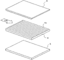
図2は、前述の構成のバックライトユニット1における導光板4、反射シート5及び光学シート(特に、プリズムシート8)の重ね合わせ状態を示すものである。導光板4の上面は、プリズム山4aが形成されてプリズム面とされており、前記プリズム山4aの形成方向が発光ダイオード2からの光の入光方向と概ね平行となるように設置されている。
FIG. 2 shows an overlapping state of the
導光板4の下面は、いわゆるパターン面とされており、当該パターン面と対向して反射シート5が重ねられている。一方、導光板4の上面(プリズム面)上には、プリズムシート8がプリズム面同士が対向し、且つプリズム山の形成方向が互いに略直交するように重ねられている。これら構成により、導光板4の端面から入光された光は、導光板4のプリズム面から出射され、プリズムシート8を介して例えば液晶表示パネル等に効率的に照射される。また、導光板4の上面がプリズム面とされているので、プリズムシートを1枚省略することができ、部品点数を削減することができる。
The lower surface of the
ここで、前記導光板4の上面をプリズム面とする場合、先ず第1に、図3に示すように、プリズム山4aが連続する形で形成(プリズム山4a間に平坦面が無い状態で形成)することが考えられる。この場合には、光の伝搬等の点で不満が残る可能性があり、また、プリズム金型の傷つきの問題が生じたり、導光板4のプリズム面とプリズムシート8のプリズム面の密着具合によっては貼り付きムラが発生する等、表示品位を低下する原因となるおそれがある。
Here, when the upper surface of the
そこで、本発明においては、図4に示すように、導光板4のプリズム面において、連続して形成されていたプリズム山4aの一部を削減し、プリズム山4a間に平坦面4bを形成するようにしている。この場合、プリズム山4aの形成ピッチは、例えば30μm程度であり、プリズム山4aの幅は15μm程度、平坦面4bの幅は5〜10μm程度(例えば、6,7μm)とすればよい。勿論、これに限らず、寸法は要求される光学特性等に応じて適宜設定すればよいが、前記平坦面4bの幅は、最低でも2,3μmとすることが好ましい。
Therefore, in the present invention, as shown in FIG. 4, a part of the
前述のように、導光板4のプリズム面において、プリズム山4a間に平坦面4bを形成することにより、光の伝搬が良好なものとなり、導光板4の面内において、場所によって暗くなる等の問題を改善することができる。
As described above, by forming the
ただし、プリズム山4a間に平坦面4bを形成した場合、プリズム面の機能が低下することになり、例えば輝度が低下する等の問題が生ずる。また、平坦面4bに傷が形成されると、面光源として見た場合に傷が目立つという問題もある。
However, when the
そこで、本実施形態の導光板4では、前記平坦面4bに微細な凹凸面を形成し、いわゆる粗面化することで、前記問題を解消するようにしている。プリズム山4a間の平坦面4bを粗面化することで、輝度を向上することができ、平坦面4bに傷が入った場合にも、目立たなくすることができる。
Therefore, in the
前記平坦面4bに形成する微細な凹凸(粗面)は、平坦面4bを散乱面とすることができるものであれば如何なるものであってもよく、いわゆる梨地面のように、ブラスト処理等の粗面化処理によって形成される微細凹凸面であってもよい。凹凸の深さも任意であるが、例えば0.5μm程度とすることが好ましい。
The fine unevenness (rough surface) formed on the
前記凹凸形成(粗面化)は、前記平坦面4bに施せばよいが、さらにプリズム山4aも含めてプリズム面全体に施すことも可能である。例えばブラスト処理等により粗面化する場合、プリズム面全体を粗面化する方が簡単に行うことが可能である。なお、プリズム面全体に粗面化処理を施すと、プリズムの機能が低下する可能性もあるので、この点を考慮すると、平坦面4bにのみ凹凸を形成し粗面化することが好ましい。
The unevenness formation (roughening) may be performed on the
平坦面4bにのみ凹凸を形成し粗面化するには、例えば導光板4を成形する際に使用する金型を形成するに際し、金型母材のプリズム面に対応する面を予めブラスト処理等により全面粗面化処理しておき、ここにプリズム山4aに対応する断面三角形の溝を形成すればよい。断面三角形の溝を形成する際に鏡面加工すれば、プリズム山4aの表面は鏡面化され、プリズム山4a間の平坦面4bは、前記金型母材の粗面化処理によって凹凸面(粗面)とされる。
In order to form unevenness only on the
また、平坦面4bを粗面化するに当たって、凹凸の密度を場所によって変えることで、輝度ムラの解消を図ることも可能である。例えば、平坦面4bを粗面化した場合、凹凸の密度が高いほど輝度向上の効果が大きい。したがって、導光板4の面内において、暗い部分の凹凸密度を高めることで、相対的な輝度の差を解消することができ、輝度ムラが解消される。
Further, when the
例えば、図5に示すように、発光ダイオード2の光が入光される端面4c近傍の輝度が発光ダイオード2の光の直進性によって他の部分よりも低い場合には、平坦面4bの前記端面4cに近い部分4dに形成される凹凸密度を他の部分より高めることで、この部分の輝度を向上することができ、導光板4全体の輝度を均一にすることが可能になる。あるいは、発光ダイオード2の配列方向の両端部において輝度が低い場合には、図6に示すように、プリズム山4aの配列方向の両端に位置する平坦面4fにおける凹凸密度を他の平坦面4bに比べて高くすることで、やはり導光板4全体の輝度を均一にすることが可能になる。また、図5及び図6に示す構成を組み合わせて、両者の凹凸を混在させて構成すれば、より導光板4の輝度の均一化に貢献させることが可能となる。
For example, as shown in FIG. 5, when the luminance in the vicinity of the
以上の構成を有するバックライトユニット1は、液晶表示装置において、面光源装置として組み込まれる。そこで次に、前述のバックライトユニット1を組み込んだ液晶表示装置について説明する。
The
図7は、面光源装置であるバックライトユニット1が組み込まれた液晶表示装置を分解して示すものである。本実施形態の液晶表示装置は、図7に示すように、液晶表示パネル21と前述のバックライトユニット1とを備え、これらを金属材料や樹脂材料等で形成された外筐22(フロントケースは図示省略)で保持するようにしている。
FIG. 7 is an exploded view of a liquid crystal display device in which the
液晶表示パネル21は、例えばアレイ基板と対向基板の間に液晶材料を封入することにより構成され、アレイ基板には表示画素に対応して画素電極及びスイッチング素子(薄膜トランジスタ)がマトリクス状に形成されている。また、アレイ基板には、画素電極に電気信号を送るための信号線と、スイッチング素子である薄膜トランジスタにスイッチング信号を供給するためのゲート線とが互いに直交して配線されている。一方、対向基板には、対向電極が透明電極材料(例えばITO等)によりほぼ全面に形成されており、各画素に対応してカラーフィルタ層が形成されている。さらに、前記アレイ基板と対向基板の外表面には、それぞれ偏光板が偏光軸を互いに直交させて貼り合わされている。
The liquid
液晶表示パネル21の額縁領域には、薄膜トランジスタ等の駆動トランジスタを備え駆動信号を供給する駆動回路部が形成されており、外部回路基板からの駆動信号に基づいて前記スイッチング素子が駆動されることで画像表示が行われる。この画像表示が行われる領域が表示領域であり、前記液晶表示パネル21は多数の画素が配列された表示領域を有する。
In the frame area of the liquid
前記バックライトユニット1は、前記液晶表示パネル21の光源として組み込まれるものであり、発光ダイオード2から出射された光は、導光板4へ導かれ、導光板4のプリズム面から出射され、プリズムシート8を含む光学シート6を介して、平面光として液晶表示パネル21の有効表示エリアに照射される。液晶表示パネル21では照射された光が透過もしくは遮断され、文字や映像等の画像が所定の明るさで表示される。
The
前述の液晶表示装置においては、本発明のバックライトユニット1を組み込んでいるので、輝度が高く表示品位の高い液晶表示装置を実現することが可能である。また、部品点数が少なくて済むので、製造コストを低減し、生産性を向上することができるというメリットも有する。
Since the above-described liquid crystal display device incorporates the
1 バックライトユニット、2 発光ダイオード、3 フレキシブル配線基板、4 導光板、4a プリズム山、4b 平坦面、5 反射シート、6 光学シート、7 バックケース、8 プリズムシート、21 液晶表示パネル、22 外筺
DESCRIPTION OF
Claims (5)
前記導光板の光出射面は、断面三角形の複数のプリズム山が略平行に配列されてプリズム面とされており、
前記各プリズム山間に平坦面が配置されるとともに、前記平坦面が粗面化されていることを特徴とする面光源装置。 A surface light source device comprising a light source and a light guide plate that converts light from the light source into planar light,
The light exit surface of the light guide plate is a prism surface in which a plurality of prism peaks having a triangular cross section are arranged substantially in parallel.
A surface light source device, wherein a flat surface is disposed between the prism peaks, and the flat surface is roughened.
Priority Applications (1)
| Application Number | Priority Date | Filing Date | Title |
|---|---|---|---|
| JP2009093322A JP2010244902A (en) | 2009-04-07 | 2009-04-07 | Surface light source device and liquid crystal display device provided with the surface light source device |
Applications Claiming Priority (1)
| Application Number | Priority Date | Filing Date | Title |
|---|---|---|---|
| JP2009093322A JP2010244902A (en) | 2009-04-07 | 2009-04-07 | Surface light source device and liquid crystal display device provided with the surface light source device |
Publications (1)
| Publication Number | Publication Date |
|---|---|
| JP2010244902A true JP2010244902A (en) | 2010-10-28 |
Family
ID=43097689
Family Applications (1)
| Application Number | Title | Priority Date | Filing Date |
|---|---|---|---|
| JP2009093322A Pending JP2010244902A (en) | 2009-04-07 | 2009-04-07 | Surface light source device and liquid crystal display device provided with the surface light source device |
Country Status (1)
| Country | Link |
|---|---|
| JP (1) | JP2010244902A (en) |
Cited By (3)
| Publication number | Priority date | Publication date | Assignee | Title |
|---|---|---|---|---|
| JP2012252340A (en) * | 2011-06-03 | 2012-12-20 | Gunko Kagi (Shenzhen) Yugenkoshi | Optical sheet, method for manufacturing the same, and liquid crystal display device using the same |
| KR101551648B1 (en) | 2013-10-23 | 2015-09-09 | (주)휴넷플러스 | Integrated light guide pannel |
| TWI627475B (en) * | 2017-05-31 | 2018-06-21 | 蘇州璨宇光學有限公司 | Backlight module |
-
2009
- 2009-04-07 JP JP2009093322A patent/JP2010244902A/en active Pending
Cited By (3)
| Publication number | Priority date | Publication date | Assignee | Title |
|---|---|---|---|---|
| JP2012252340A (en) * | 2011-06-03 | 2012-12-20 | Gunko Kagi (Shenzhen) Yugenkoshi | Optical sheet, method for manufacturing the same, and liquid crystal display device using the same |
| KR101551648B1 (en) | 2013-10-23 | 2015-09-09 | (주)휴넷플러스 | Integrated light guide pannel |
| TWI627475B (en) * | 2017-05-31 | 2018-06-21 | 蘇州璨宇光學有限公司 | Backlight module |
Similar Documents
| Publication | Publication Date | Title |
|---|---|---|
| KR100978078B1 (en) | Prism sheet and liquid crystal display device having same | |
| CN102003658A (en) | Optical sheet, backlight unit and liquid crystal display device having the same and method of fabricating optical sheet | |
| TW201104320A (en) | Backlight unit | |
| CN102597603A (en) | Planar lighting device and display apparatus provided with same | |
| US20110090427A1 (en) | Light guide plate, backlight device and liquid crystal display device | |
| CN101477272A (en) | Optical plate, backlight assembly and display device including the same | |
| CN106019667A (en) | Display device | |
| KR20110064743A (en) | Backlight unit and liquid crystal display device having same | |
| CN103133945A (en) | Backlight module for providing light source to display panel and display device thereof | |
| WO2016194716A1 (en) | Edge-lit backlight device and liquid crystal display device | |
| JP2012238431A (en) | Edge-light type backlight unit, and liquid crystal module using the same | |
| JP2009117272A (en) | Liquid crystal display device | |
| WO2015136625A1 (en) | Light source apparatus, display apparatus, and light source apparatus manufacturing method | |
| KR102087965B1 (en) | Backlight assembly and display device comprising the same | |
| KR20090086759A (en) | A prism sheet having a prism acid having a longitudinal wave pattern with improved front luminance, a backlight unit employing the same, and a liquid crystal display device having the backlight unit. | |
| CN105652352B (en) | Prismatic lens and liquid crystal display device with the prismatic lens | |
| JP6266803B2 (en) | Light guide unit, light source device, and display device | |
| CN103105695A (en) | Liquid crystal panel assembly and image display apparatus having the same | |
| KR102030412B1 (en) | Light guide plate having rounded polyggon pattern and liquid cyrstal display device having thereof | |
| US7471354B2 (en) | Backlight module and liquid crystal display | |
| TWI405102B (en) | Backlight module and optical touch panel | |
| KR100838332B1 (en) | Backlight structure for flat panel display | |
| JP7249779B2 (en) | Displays and electronics | |
| JP2012154970A (en) | Liquid crystal module | |
| JP5492519B2 (en) | Backlight unit and video display device using the same |