JP2010263109A - 受発光装置 - Google Patents
受発光装置 Download PDFInfo
- Publication number
- JP2010263109A JP2010263109A JP2009113492A JP2009113492A JP2010263109A JP 2010263109 A JP2010263109 A JP 2010263109A JP 2009113492 A JP2009113492 A JP 2009113492A JP 2009113492 A JP2009113492 A JP 2009113492A JP 2010263109 A JP2010263109 A JP 2010263109A
- Authority
- JP
- Japan
- Prior art keywords
- light
- layer
- light receiving
- electrode
- light emitting
- Prior art date
- Legal status (The legal status is an assumption and is not a legal conclusion. Google has not performed a legal analysis and makes no representation as to the accuracy of the status listed.)
- Granted
Links
Images




Classifications
-
- H—ELECTRICITY
- H10—SEMICONDUCTOR DEVICES; ELECTRIC SOLID-STATE DEVICES NOT OTHERWISE PROVIDED FOR
- H10F—INORGANIC SEMICONDUCTOR DEVICES SENSITIVE TO INFRARED RADIATION, LIGHT, ELECTROMAGNETIC RADIATION OF SHORTER WAVELENGTH OR CORPUSCULAR RADIATION
- H10F99/00—Subject matter not provided for in other groups of this subclass
-
- H—ELECTRICITY
- H01—ELECTRIC ELEMENTS
- H01S—DEVICES USING THE PROCESS OF LIGHT AMPLIFICATION BY STIMULATED EMISSION OF RADIATION [LASER] TO AMPLIFY OR GENERATE LIGHT; DEVICES USING STIMULATED EMISSION OF ELECTROMAGNETIC RADIATION IN WAVE RANGES OTHER THAN OPTICAL
- H01S5/00—Semiconductor lasers
- H01S5/02—Structural details or components not essential to laser action
- H01S5/026—Monolithically integrated components, e.g. waveguides, monitoring photo-detectors, drivers
- H01S5/0262—Photo-diodes, e.g. transceiver devices, bidirectional devices
-
- H—ELECTRICITY
- H10—SEMICONDUCTOR DEVICES; ELECTRIC SOLID-STATE DEVICES NOT OTHERWISE PROVIDED FOR
- H10F—INORGANIC SEMICONDUCTOR DEVICES SENSITIVE TO INFRARED RADIATION, LIGHT, ELECTROMAGNETIC RADIATION OF SHORTER WAVELENGTH OR CORPUSCULAR RADIATION
- H10F30/00—Individual radiation-sensitive semiconductor devices in which radiation controls the flow of current through the devices, e.g. photodetectors
- H10F30/20—Individual radiation-sensitive semiconductor devices in which radiation controls the flow of current through the devices, e.g. photodetectors the devices having potential barriers, e.g. phototransistors
- H10F30/21—Individual radiation-sensitive semiconductor devices in which radiation controls the flow of current through the devices, e.g. photodetectors the devices having potential barriers, e.g. phototransistors the devices being sensitive to infrared, visible or ultraviolet radiation
- H10F30/22—Individual radiation-sensitive semiconductor devices in which radiation controls the flow of current through the devices, e.g. photodetectors the devices having potential barriers, e.g. phototransistors the devices being sensitive to infrared, visible or ultraviolet radiation the devices having only one potential barrier, e.g. photodiodes
- H10F30/221—Individual radiation-sensitive semiconductor devices in which radiation controls the flow of current through the devices, e.g. photodetectors the devices having potential barriers, e.g. phototransistors the devices being sensitive to infrared, visible or ultraviolet radiation the devices having only one potential barrier, e.g. photodiodes the potential barrier being a PN homojunction
- H10F30/2215—Individual radiation-sensitive semiconductor devices in which radiation controls the flow of current through the devices, e.g. photodetectors the devices having potential barriers, e.g. phototransistors the devices being sensitive to infrared, visible or ultraviolet radiation the devices having only one potential barrier, e.g. photodiodes the potential barrier being a PN homojunction the devices comprising active layers made of only Group III-V materials
-
- H—ELECTRICITY
- H10—SEMICONDUCTOR DEVICES; ELECTRIC SOLID-STATE DEVICES NOT OTHERWISE PROVIDED FOR
- H10F—INORGANIC SEMICONDUCTOR DEVICES SENSITIVE TO INFRARED RADIATION, LIGHT, ELECTROMAGNETIC RADIATION OF SHORTER WAVELENGTH OR CORPUSCULAR RADIATION
- H10F30/00—Individual radiation-sensitive semiconductor devices in which radiation controls the flow of current through the devices, e.g. photodetectors
- H10F30/20—Individual radiation-sensitive semiconductor devices in which radiation controls the flow of current through the devices, e.g. photodetectors the devices having potential barriers, e.g. phototransistors
- H10F30/21—Individual radiation-sensitive semiconductor devices in which radiation controls the flow of current through the devices, e.g. photodetectors the devices having potential barriers, e.g. phototransistors the devices being sensitive to infrared, visible or ultraviolet radiation
- H10F30/22—Individual radiation-sensitive semiconductor devices in which radiation controls the flow of current through the devices, e.g. photodetectors the devices having potential barriers, e.g. phototransistors the devices being sensitive to infrared, visible or ultraviolet radiation the devices having only one potential barrier, e.g. photodiodes
- H10F30/223—Individual radiation-sensitive semiconductor devices in which radiation controls the flow of current through the devices, e.g. photodetectors the devices having potential barriers, e.g. phototransistors the devices being sensitive to infrared, visible or ultraviolet radiation the devices having only one potential barrier, e.g. photodiodes the potential barrier being a PIN barrier
-
- H—ELECTRICITY
- H10—SEMICONDUCTOR DEVICES; ELECTRIC SOLID-STATE DEVICES NOT OTHERWISE PROVIDED FOR
- H10F—INORGANIC SEMICONDUCTOR DEVICES SENSITIVE TO INFRARED RADIATION, LIGHT, ELECTROMAGNETIC RADIATION OF SHORTER WAVELENGTH OR CORPUSCULAR RADIATION
- H10F55/00—Radiation-sensitive semiconductor devices covered by groups H10F10/00, H10F19/00 or H10F30/00 being structurally associated with electric light sources and electrically or optically coupled thereto
- H10F55/20—Radiation-sensitive semiconductor devices covered by groups H10F10/00, H10F19/00 or H10F30/00 being structurally associated with electric light sources and electrically or optically coupled thereto wherein the electric light source controls the radiation-sensitive semiconductor devices, e.g. optocouplers
- H10F55/25—Radiation-sensitive semiconductor devices covered by groups H10F10/00, H10F19/00 or H10F30/00 being structurally associated with electric light sources and electrically or optically coupled thereto wherein the electric light source controls the radiation-sensitive semiconductor devices, e.g. optocouplers wherein the radiation-sensitive devices and the electric light source are all semiconductor devices
- H10F55/255—Radiation-sensitive semiconductor devices covered by groups H10F10/00, H10F19/00 or H10F30/00 being structurally associated with electric light sources and electrically or optically coupled thereto wherein the electric light source controls the radiation-sensitive semiconductor devices, e.g. optocouplers wherein the radiation-sensitive devices and the electric light source are all semiconductor devices formed in, or on, a common substrate
-
- H—ELECTRICITY
- H10—SEMICONDUCTOR DEVICES; ELECTRIC SOLID-STATE DEVICES NOT OTHERWISE PROVIDED FOR
- H10H—INORGANIC LIGHT-EMITTING SEMICONDUCTOR DEVICES HAVING POTENTIAL BARRIERS
- H10H29/00—Integrated devices, or assemblies of multiple devices, comprising at least one light-emitting semiconductor element covered by group H10H20/00
- H10H29/10—Integrated devices comprising at least one light-emitting semiconductor component covered by group H10H20/00
-
- H—ELECTRICITY
- H10—SEMICONDUCTOR DEVICES; ELECTRIC SOLID-STATE DEVICES NOT OTHERWISE PROVIDED FOR
- H10H—INORGANIC LIGHT-EMITTING SEMICONDUCTOR DEVICES HAVING POTENTIAL BARRIERS
- H10H20/00—Individual inorganic light-emitting semiconductor devices having potential barriers, e.g. light-emitting diodes [LED]
- H10H20/80—Constructional details
- H10H20/81—Bodies
- H10H20/813—Bodies having a plurality of light-emitting regions, e.g. multi-junction LEDs or light-emitting devices having photoluminescent regions within the bodies
-
- H—ELECTRICITY
- H10—SEMICONDUCTOR DEVICES; ELECTRIC SOLID-STATE DEVICES NOT OTHERWISE PROVIDED FOR
- H10H—INORGANIC LIGHT-EMITTING SEMICONDUCTOR DEVICES HAVING POTENTIAL BARRIERS
- H10H20/00—Individual inorganic light-emitting semiconductor devices having potential barriers, e.g. light-emitting diodes [LED]
- H10H20/80—Constructional details
- H10H20/81—Bodies
- H10H20/822—Materials of the light-emitting regions
- H10H20/824—Materials of the light-emitting regions comprising only Group III-V materials, e.g. GaP
Landscapes
- Physics & Mathematics (AREA)
- Electromagnetism (AREA)
- Condensed Matter Physics & Semiconductors (AREA)
- General Physics & Mathematics (AREA)
- Optics & Photonics (AREA)
- Light Receiving Elements (AREA)
- Led Devices (AREA)
- Photo Coupler, Interrupter, Optical-To-Optical Conversion Devices (AREA)
Abstract
【解決手段】同一基板上に設けられた発光部100と受光部200a,200bとを含み、発光部は、第1クラッド層および第2クラッド層に挟まれた活性層と、第1クラッド層に電気的に接続された第1電極と、第2クラッド層に電気的に接続された第2電極と、を有し、受光部は、光吸収層を有し、活性層の少なくとも一部は、第1電極と第2電極の間の電流経路に利得領域140を構成し、利得領域は、活性層の第1側面105から第1側面と平行な第2側面107まで、第1側面の垂線に対して傾いた方向に向かって設けられ、利得領域に生じる光は、利得領域の第1側面側の端面151および第2側面側の端面152の少なくとも一方において、外部に出射される光と、反射される光と、に分けられ、反射される光は、受光部において受光される。
【選択図】図1
Description
同一基板上に設けられた発光部と受光部とを含み、
前記発光部は、
第1クラッド層および第2クラッド層に挟まれた活性層と、
前記第1クラッド層に電気的に接続された第1電極と、
前記第2クラッド層に電気的に接続された第2電極と、
を有し、
前記受光部は、光吸収層を有し、
前記活性層の少なくとも一部は、前記第1電極と前記第2電極の間の電流経路に利得領域を構成し、
前記利得領域は、平面的に見て、前記活性層の第1側面から前記第1側面と平行な第2側面まで、前記第1側面の垂線に対して傾いた方向に向かって設けられ、
前記利得領域に生じる光は、前記利得領域の前記第1側面側の端面および前記第2側面側の端面の少なくとも一方において、外部に出射される光と、反射される光と、に分けられ、
前記反射される光は、前記受光部において受光される。
方」という文言を用いている。
前記受光部は、前記第1側面側と前記第2側面側とに設けられていることができる。
前記発光部と前記受光部とを電気的に分離する分離溝を有することができる。
前記分離溝は、平面的に見て、前記受光部の周囲を囲んでいることができる。
前記活性層と前記光吸収層は、連続した1つの層であることができる。
前記活性層の下面の位置は、前記光吸収層の下面の位置より上方であり、
前記活性層の上面の位置は、前記光吸収層の上面の位置より下方であることができる。
前記利得領域では、前記第1側面側から平面的に見て、前記第1側面側の端面と、前記第2側面側の端面とは、重なっていないことができる。
前記利得領域は、複数配列され、
複数の前記利得領域の各々に対応して、前記受光部が設けられていることができる。
まず、本実施形態に係る受発光装置1000について説明する。
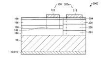
発光部100は、図2に示すように、第1クラッド層104および第2クラッド層108に挟まれた活性層106と、第1電極120と、第2電極122と、を有する。発光部100は、さらに、第1コンタクト層109を有することができる。
受光部200a,200bは、図1および図2に示すように、光吸収層206を含む。受光部200a,200bは、さらに、例えば、第3クラッド層204と、第4クラッド層208と、第2コンタクト層209と、第3電極210と、第4電極212と、を有することができる。
受発光装置1000の発光部100では、第1電極120と第2電極122との間に、pinダイオードの順バイアス電圧を印加すると、活性層106の利得領域140において電子と正孔との再結合が起こる。この再結合により発光が生じる。この生じた光を起点として、連鎖的に誘導放出が起こり、利得領域140内で光の強度が増幅される。例えば、図1に示すように、利得領域140に生じる光のうち、第1端面151に向かう光2は、利得領域140内で増幅された後、第1端面151から第1出射光2aとして出射される。同様に、利得領域140に生じる光のうち、第2端面152に向かう光4は、利得領域140内で増幅された後、第2端面152から第2出射光4aとして出射される。ここで、第1端面151に向かう光2および第2端面152に向かう光4の一部は、第1端面151および第2端面152で反射され、第1反射光2bおよび第2反射光4bとして受発光装置1000内を進行するものもある。すなわち、利得領域140に生じる光のうち、第1端面151に向かう光2は、第1端面151において、第1出射光2aと、第1反射光2bとに分けられる。第2端面152に向かう光4についても同様に、第2端面152において、第2出射光4aと、第2反射光4bとに分けられる。第1反射光2bは、受発光装置1000内を進行して第1受光部200aに至る。第2反射光4bも同様に、受発光装置1000内を進行して第2受光部200bに至る。なお、図1の例では、第1端面151および第2端面152の両方から光が出射される場合について説明したが、いずれか一方の端面から光が出射されてもよい。
次に、受発光装置1000の製造方法の一例について、図面を参照しながら説明する。
次に本実施形態に係る受発光装置の変形例について説明する。なお、上述した図1〜図2に示す受発光装置1000の例と異なる点について説明し、同様の点については同一の符号を付し説明を省略する。
まず、第1の変形例について説明する。
次に、第2の変形例について説明する。
次に、第3の変形例について説明する。
次に、第4の変形例について説明する。
Claims (8)
- 同一基板上に設けられた発光部と受光部とを含み、
前記発光部は、
第1クラッド層および第2クラッド層に挟まれた活性層と、
前記第1クラッド層に電気的に接続された第1電極と、
前記第2クラッド層に電気的に接続された第2電極と、
を有し、
前記受光部は、光吸収層を有し、
前記活性層の少なくとも一部は、前記第1電極と前記第2電極の間の電流経路に利得領域を構成し、
前記利得領域は、平面的に見て、前記活性層の第1側面から前記第1側面と平行な第2側面まで、前記第1側面の垂線に対して傾いた方向に向かって設けられ、
前記利得領域に生じる光は、前記利得領域の前記第1側面側の端面および前記第2側面側の端面の少なくとも一方において、外部に出射される光と、反射される光と、に分けられ、
前記反射される光は、前記受光部において受光される、受発光装置。 - 請求項1において、
前記受光部は、前記第1側面側と前記第2側面側とに設けられている、受発光装置。 - 請求項1または2において、
前記発光部と前記受光部とを電気的に分離する分離溝を有する、受発光装置。 - 請求項3において、
前記分離溝は、平面的に見て、前記受光部を周囲を囲んでいる、受発光装置。 - 請求項1乃至4のいずれか一項において、
前記活性層と前記光吸収層は、連続した1つの層である、受発光装置。 - 請求項1乃至5のいずれか一項において、
前記活性層の下面の位置は、前記光吸収層の下面の位置より上方であり、
前記活性層の上面の位置は、前記光吸収層の上面の位置より下方である、受発光装置。 - 請求項1乃至6のいずれか一項において、
前記利得領域では、前記第1側面側から平面的に見て、前記第1側面側の端面と、前記第2側面側の端面とは、重なっていない、発光装置。 - 請求項1乃至7のいずれか一項において、
前記利得領域は、複数配列され、
複数の前記利得領域の各々に対応して、前記受光部が設けられている、受発光装置。
Priority Applications (3)
| Application Number | Priority Date | Filing Date | Title |
|---|---|---|---|
| JP2009113492A JP5447794B2 (ja) | 2009-05-08 | 2009-05-08 | 発光装置 |
| US12/767,103 US8344393B2 (en) | 2009-05-08 | 2010-04-26 | Light receiving and emitting device |
| US13/693,624 US8629461B2 (en) | 2009-05-08 | 2012-12-04 | Light receiving and emitting device |
Applications Claiming Priority (1)
| Application Number | Priority Date | Filing Date | Title |
|---|---|---|---|
| JP2009113492A JP5447794B2 (ja) | 2009-05-08 | 2009-05-08 | 発光装置 |
Publications (3)
| Publication Number | Publication Date |
|---|---|
| JP2010263109A true JP2010263109A (ja) | 2010-11-18 |
| JP2010263109A5 JP2010263109A5 (ja) | 2012-06-21 |
| JP5447794B2 JP5447794B2 (ja) | 2014-03-19 |
Family
ID=43061841
Family Applications (1)
| Application Number | Title | Priority Date | Filing Date |
|---|---|---|---|
| JP2009113492A Expired - Fee Related JP5447794B2 (ja) | 2009-05-08 | 2009-05-08 | 発光装置 |
Country Status (2)
| Country | Link |
|---|---|
| US (2) | US8344393B2 (ja) |
| JP (1) | JP5447794B2 (ja) |
Cited By (1)
| Publication number | Priority date | Publication date | Assignee | Title |
|---|---|---|---|---|
| US8727031B2 (en) | 2008-12-12 | 2014-05-20 | Amrona Ag | System and method for preventing or extinguishing fire |
Families Citing this family (8)
| Publication number | Priority date | Publication date | Assignee | Title |
|---|---|---|---|---|
| JP5447794B2 (ja) * | 2009-05-08 | 2014-03-19 | セイコーエプソン株式会社 | 発光装置 |
| JP5447799B2 (ja) * | 2009-06-18 | 2014-03-19 | セイコーエプソン株式会社 | 発光装置およびその駆動方法、並びに、プロジェクター |
| ITMI20111446A1 (it) * | 2011-07-29 | 2013-01-30 | E T C Srl | Transistor organico elettroluminescente |
| ITMI20111447A1 (it) | 2011-07-29 | 2013-01-30 | E T C Srl | Transistor organico elettroluminescente |
| US20140184062A1 (en) * | 2012-12-27 | 2014-07-03 | GE Lighting Solutions, LLC | Systems and methods for a light emitting diode chip |
| US10022741B2 (en) | 2014-08-22 | 2018-07-17 | Nse Products, Inc. | Selectively actuated fluid dispenser |
| US10840406B2 (en) * | 2017-04-17 | 2020-11-17 | Hamamatsu Photonics K.K. | Optical semiconductor element and method of driving optical semiconductor element |
| WO2025117622A1 (en) * | 2023-11-27 | 2025-06-05 | Massachusetts Institute Of Technology | An integrated pixel cell for a display device and/or optical communication device |
Citations (2)
| Publication number | Priority date | Publication date | Assignee | Title |
|---|---|---|---|---|
| JPH0426159A (ja) * | 1990-05-22 | 1992-01-29 | Ricoh Co Ltd | 半導体光集積装置 |
| JP2005216954A (ja) * | 2004-01-27 | 2005-08-11 | Sumitomo Electric Ind Ltd | 半導体光素子 |
Family Cites Families (11)
| Publication number | Priority date | Publication date | Assignee | Title |
|---|---|---|---|---|
| JPH0433386A (ja) | 1990-05-30 | 1992-02-04 | Omron Corp | 端面出射型半導体発光素子およびその駆動方法 |
| JPH08162669A (ja) | 1994-12-06 | 1996-06-21 | Nippondenso Co Ltd | スーパールミネッセントダイオード |
| JPH103691A (ja) | 1996-04-18 | 1998-01-06 | Matsushita Electric Ind Co Ltd | 光ピックアップ装置 |
| US6459716B1 (en) * | 2001-02-01 | 2002-10-01 | Nova Crystals, Inc. | Integrated surface-emitting laser and modulator device |
| KR100575964B1 (ko) * | 2003-12-16 | 2006-05-02 | 삼성전자주식회사 | 광검출기가 모놀리식 집적된 전계 흡수형 광변조 모듈 |
| JP5168476B2 (ja) | 2008-03-26 | 2013-03-21 | セイコーエプソン株式会社 | 発光装置 |
| JP5411440B2 (ja) | 2008-03-26 | 2014-02-12 | セイコーエプソン株式会社 | 発光装置 |
| JP2009238846A (ja) | 2008-03-26 | 2009-10-15 | Seiko Epson Corp | 発光装置 |
| JP2009238845A (ja) | 2008-03-26 | 2009-10-15 | Seiko Epson Corp | 発光モジュール及びその製造方法 |
| JP5382289B2 (ja) | 2008-03-26 | 2014-01-08 | セイコーエプソン株式会社 | 発光装置 |
| JP5447794B2 (ja) * | 2009-05-08 | 2014-03-19 | セイコーエプソン株式会社 | 発光装置 |
-
2009
- 2009-05-08 JP JP2009113492A patent/JP5447794B2/ja not_active Expired - Fee Related
-
2010
- 2010-04-26 US US12/767,103 patent/US8344393B2/en not_active Expired - Fee Related
-
2012
- 2012-12-04 US US13/693,624 patent/US8629461B2/en not_active Expired - Fee Related
Patent Citations (2)
| Publication number | Priority date | Publication date | Assignee | Title |
|---|---|---|---|---|
| JPH0426159A (ja) * | 1990-05-22 | 1992-01-29 | Ricoh Co Ltd | 半導体光集積装置 |
| JP2005216954A (ja) * | 2004-01-27 | 2005-08-11 | Sumitomo Electric Ind Ltd | 半導体光素子 |
Cited By (1)
| Publication number | Priority date | Publication date | Assignee | Title |
|---|---|---|---|---|
| US8727031B2 (en) | 2008-12-12 | 2014-05-20 | Amrona Ag | System and method for preventing or extinguishing fire |
Also Published As
| Publication number | Publication date |
|---|---|
| US20130092959A1 (en) | 2013-04-18 |
| US8629461B2 (en) | 2014-01-14 |
| US8344393B2 (en) | 2013-01-01 |
| JP5447794B2 (ja) | 2014-03-19 |
| US20100283063A1 (en) | 2010-11-11 |
Similar Documents
| Publication | Publication Date | Title |
|---|---|---|
| JP5447794B2 (ja) | 発光装置 | |
| JP5196179B2 (ja) | 発光装置 | |
| JP2010263109A5 (ja) | ||
| US8467427B2 (en) | Light emitting and receiving device | |
| US20100232467A1 (en) | Light emitting device | |
| JP5088498B2 (ja) | 発光装置 | |
| JP5187525B2 (ja) | 発光装置 | |
| JP5382289B2 (ja) | 発光装置 | |
| JP2010016172A (ja) | 発光装置 | |
| US8194714B2 (en) | Light emitting and receiving device | |
| JP2011066138A (ja) | プロジェクター | |
| JP2010212347A (ja) | 受発光装置 | |
| JP2010225737A (ja) | 発光装置および発光モジュール | |
| JP2009238845A (ja) | 発光モジュール及びその製造方法 | |
| JP2010141241A (ja) | 発光装置の製造方法および発光装置 | |
| JP2010161104A (ja) | 発光装置および積層型発光装置 | |
| JP5168476B2 (ja) | 発光装置 | |
| JP2009238846A (ja) | 発光装置 | |
| JP5534259B2 (ja) | 発光装置 | |
| JP2010219199A (ja) | 受発光装置 | |
| JP5403305B2 (ja) | 発光装置 | |
| JP2010267642A (ja) | 発光装置 | |
| JP2010212348A (ja) | 発光装置 | |
| JP2015087693A (ja) | 発光装置およびプロジェクター | |
| JP2009238827A (ja) | 発光装置 |
Legal Events
| Date | Code | Title | Description |
|---|---|---|---|
| A521 | Request for written amendment filed |
Free format text: JAPANESE INTERMEDIATE CODE: A523 Effective date: 20120502 |
|
| A621 | Written request for application examination |
Free format text: JAPANESE INTERMEDIATE CODE: A621 Effective date: 20120502 |
|
| A131 | Notification of reasons for refusal |
Free format text: JAPANESE INTERMEDIATE CODE: A131 Effective date: 20130724 |
|
| A977 | Report on retrieval |
Free format text: JAPANESE INTERMEDIATE CODE: A971007 Effective date: 20130724 |
|
| A521 | Request for written amendment filed |
Free format text: JAPANESE INTERMEDIATE CODE: A523 Effective date: 20130924 |
|
| TRDD | Decision of grant or rejection written | ||
| A01 | Written decision to grant a patent or to grant a registration (utility model) |
Free format text: JAPANESE INTERMEDIATE CODE: A01 Effective date: 20131204 |
|
| A61 | First payment of annual fees (during grant procedure) |
Free format text: JAPANESE INTERMEDIATE CODE: A61 Effective date: 20131217 |
|
| R150 | Certificate of patent or registration of utility model |
Free format text: JAPANESE INTERMEDIATE CODE: R150 |
|
| S531 | Written request for registration of change of domicile |
Free format text: JAPANESE INTERMEDIATE CODE: R313531 |
|
| R350 | Written notification of registration of transfer |
Free format text: JAPANESE INTERMEDIATE CODE: R350 |
|
| LAPS | Cancellation because of no payment of annual fees |