JP2011021237A - Transparent conductive film and method for forming the same - Google Patents
Transparent conductive film and method for forming the same Download PDFInfo
- Publication number
- JP2011021237A JP2011021237A JP2009166999A JP2009166999A JP2011021237A JP 2011021237 A JP2011021237 A JP 2011021237A JP 2009166999 A JP2009166999 A JP 2009166999A JP 2009166999 A JP2009166999 A JP 2009166999A JP 2011021237 A JP2011021237 A JP 2011021237A
- Authority
- JP
- Japan
- Prior art keywords
- transparent conductive
- conductive film
- flow rate
- target
- film
- Prior art date
- Legal status (The legal status is an assumption and is not a legal conclusion. Google has not performed a legal analysis and makes no representation as to the accuracy of the status listed.)
- Pending
Links
Images
Landscapes
- Physical Vapour Deposition (AREA)
- Non-Insulated Conductors (AREA)
- Manufacturing Of Electric Cables (AREA)
Abstract
Description
本発明は、薄型ディスプレイ、太陽電池、バイオ刺激電極などに適用可能な透明導電膜およびその形成方法に関するものである。 The present invention relates to a transparent conductive film applicable to thin displays, solar cells, biostimulation electrodes, and the like, and a method for forming the same.
現在、薄型ディスプレイのような電子機器に最も多く使用されている透明導電膜は、ITO(Indium Tin Oxide)である。しかし、ITOの主材料であるインジウムは、希少金属であるため、太陽電池用には、専らGaドープZnOやAlドープZnOなどが使用されている。 At present, the transparent conductive film most frequently used in electronic devices such as thin displays is ITO (Indium Tin Oxide). However, since indium, which is the main material of ITO, is a rare metal, Ga-doped ZnO, Al-doped ZnO, and the like are exclusively used for solar cells.
一方、より入手しやすいTiを母体材料とするTiNが、透明導電性を有することが知られている。TiNは、AuやNiなどの極薄膜を透明導電膜として流用するのに比較すれば可視光透過率は高いものの、黄金色を帯びた金属光沢を示し、透過率はあまり高くない。 On the other hand, it is known that TiN having Ti as a base material, which is easier to obtain, has transparent conductivity. TiN has a high visible light transmittance compared to diverting an ultra-thin film such as Au or Ni as a transparent conductive film, but exhibits a golden metallic luster and the transmittance is not so high.
他方、Tiを母体材料とするTiO2は無色透明であるが、絶縁体である。TiOx(x〜2)膜は、酸素欠損による導電性を示すようになるが、もしもこの膜が十分に透明で結晶構造がアナターゼ相であれば、TiOx(x〜2)膜の抵抗率は10Ωcm程度を示し、これでは透明導電膜として使えない。 On the other hand, TiO 2 having Ti as a base material is colorless and transparent, but is an insulator. The TiO x (x˜2) film exhibits conductivity due to oxygen deficiency, but if this film is sufficiently transparent and the crystal structure is anatase phase, the resistivity of the TiO x (x˜2) film Indicates about 10 Ωcm, which cannot be used as a transparent conductive film.
これに対し、最近では、TiO2にNbをドープした透明導電膜Nb:TiO2が報告されている(非特許文献1)。用いる基板の種類にも依存するが、TiO2を構成しているTi原子の一部をNb原子置き換えることにより、10-1Ωcmから10-4Ωcm台に入る程度の抵抗率が得られている。 In contrast, recently, a transparent conductive film Nb doped with Nb on TiO 2: TiO 2 has been reported (Non-Patent Document 1). Although depending on the type of substrate to be used, a resistivity that is in the range of 10 -1 Ωcm to 10 -4 Ωcm is obtained by replacing a part of Ti atoms constituting TiO 2 with Nb atoms. .
しかしながら、透明導電膜Nb:TiO2は、PLD法やスパッタ法により形成できるが、生産性に優れるスパッタ法を用いて高速成膜するのは困難であるという問題がある。金属Tiをターゲットに用いた反応性スパッタリングにおいては、ターゲット表面に金属領域が存在する間は、スパッタ速度は非常に大きい。しかしターゲット表面がすべて酸素で覆われるとスパッタ速度は急激に低下する。このように急激な変化はTiO2という材料に特有なものである。一方、TiO2ターゲットを用いてスパッタ成膜を行うには、ターゲットが相当な還元状態のTiOxを使用しない限り、十分なスパッタ速度を得ることができない。このように、透明導電膜Nb:TiO2は、スパッタ法では高速な成膜が容易ではない。 However, although the transparent conductive film Nb: TiO 2 can be formed by a PLD method or a sputtering method, there is a problem that it is difficult to form a film at a high speed using a sputtering method having excellent productivity. In reactive sputtering using metal Ti as a target, the sputtering rate is very high while a metal region exists on the target surface. However, when the entire target surface is covered with oxygen, the sputtering rate decreases rapidly. Such a rapid change is peculiar to a material called TiO 2 . On the other hand, when performing sputtering film formation using a TiO 2 target, a sufficient sputtering rate cannot be obtained unless the target uses TiO x in a considerably reduced state. Thus, the transparent conductive film Nb: TiO 2 is not easily formed at high speed by sputtering.
さらにNb:TiO2の透明導電性を発現させるためには、アナターゼ結晶の状態にすることが必要であり、成膜中あるいは成膜後に350〜500℃程度でアニールする工程が入る。よって熱に弱いプラスチック基板などは用いることができないという問題点があった。 Further, in order to develop the transparent conductivity of Nb: TiO 2 , it is necessary to be in the state of anatase crystal, and a step of annealing at about 350 to 500 ° C. is performed during or after film formation. Therefore, there is a problem that a plastic substrate which is weak against heat cannot be used.
本発明は、以上のような問題点を解消するためになされたものであり、より入手しやすいTiを母体材料とした透明導電膜の提供を目的とする。 The present invention has been made to solve the above-described problems, and an object of the present invention is to provide a transparent conductive film using Ti as a base material that is easier to obtain.
本発明に係る透明導電膜は、TiONの結晶から構成されている。ここで、結晶は、面心立方格子構造のTiOもしくはTiNの回折点(200)と同じ位置にX線の回折ピークを示す結晶性を有するものであればよい。 The transparent conductive film according to the present invention is composed of TiON crystals. Here, the crystal may have any crystallinity that exhibits an X-ray diffraction peak at the same position as the diffraction point (200) of TiO or TiN having a face-centered cubic lattice structure.
本発明に係る透明導電膜の形成方法は、不活性ガス,酸素ガス,および窒素ガスかなるプラズマを生成し、金属Tiから構成されたターゲットに負のバイアスを印加してプラズマより発生した粒子をターゲットに衝突させてスパッタ現象を起こし、ターゲットを構成する材料を基板の上に堆積することで、基板の上にTiONの結晶から構成された透明導電膜を形成する工程を備え、酸素ガスの流量は、ターゲットの表面に金属Tiが露出した状態が定常的に保持される上限の流量よりも少ない流量とする。 In the method for forming a transparent conductive film according to the present invention, a plasma composed of an inert gas, an oxygen gas, and a nitrogen gas is generated, and a negative bias is applied to a target composed of metal Ti to generate particles generated from the plasma. A process of forming a transparent conductive film composed of TiON crystals on the substrate by causing a sputtering phenomenon by colliding with the target and depositing a material constituting the target on the substrate, and a flow rate of oxygen gas The flow rate is lower than the upper limit flow rate at which the state where the metal Ti is exposed on the surface of the target is constantly maintained.
上記透明導電膜の形成方法において、透明導電膜の形成は、基板を加熱しながら行うことよい。また、プラズマは、電子サイクロトロン共鳴により生成されて発散磁界により運動エネルギーが与えられた電子サイクロトロン共鳴プラズマであるとよい。 In the method for forming a transparent conductive film, the transparent conductive film may be formed while heating the substrate. The plasma may be an electron cyclotron resonance plasma generated by electron cyclotron resonance and given kinetic energy by a divergent magnetic field.
以上説明したように、本発明によれば、透明導電膜をTiONの結晶から構成したので、より入手しやすいTiを母体材料とした透明導電膜が提供できるようになる。 As described above, according to the present invention, since the transparent conductive film is composed of TiON crystals, it is possible to provide a transparent conductive film using Ti as a base material, which is easier to obtain.
以下、本発明の実施の形態について図を参照して説明する。本発明に係る透明導電膜は、TiONの結晶から構成されたものである。この結晶は、後述するように、面心立方格子構造のTiOもしくはTiNの回折点(200)と同じ位置にX線の回折ピークを示す結晶性を有するものである。 Hereinafter, embodiments of the present invention will be described with reference to the drawings. The transparent conductive film according to the present invention is composed of TiON crystals. As will be described later, this crystal has crystallinity showing an X-ray diffraction peak at the same position as the diffraction point (200) of TiO or TiN having a face-centered cubic lattice structure.
TiOx(0<x<1)は、金属的な伝導を示すため、抵抗率は低いが透明度も低い。これに対し、TiOxは、x=1を超えて酸素量がx=2に近づくにつれて、アナターゼ相やルチル相の結晶形が現れ、抵抗率も急に高くなる。この状態では、膜の透明性は高いが、抵抗率も高い。 TiO x (0 <x <1) exhibits metallic conduction, and thus has low resistivity but low transparency. On the other hand, as TiO x exceeds x = 1 and the oxygen amount approaches x = 2, the crystal form of anatase phase or rutile phase appears, and the resistivity suddenly increases. In this state, the transparency of the film is high, but the resistivity is also high.
一方、金属Tiターゲットを用いた反応性スパッタによりTiN膜を形成する場合には、窒素ガスの流量に応じてスパッタ速度は変化するものの、酸素ガスの反応性スパッタによりTiO2膜を形成する場合に比べれば、スパッタ速度はずっと緩やかに移り変わる。TiN膜の抵抗率は窒素の導入量により変化するが、概して、抵抗率および透過率ともに低いという特徴がある。 On the other hand, when a TiN film is formed by reactive sputtering using a metal Ti target, the sputtering rate varies depending on the flow rate of nitrogen gas, but when a TiO 2 film is formed by reactive sputtering of oxygen gas. In comparison, the sputtering rate changes much more slowly. The resistivity of the TiN film varies depending on the amount of nitrogen introduced, but generally has a characteristic that both resistivity and transmittance are low.
以上の知見をもとに、TiO2の透明性とTiNの伝導性をある程度両立できるTiONを透明導電膜として利用するものとしたところに、本発明の特徴がある。また、TiONを反応性スパッタ法により形成する場合、酸素ガスと窒素ガスの流量を適切に設定することで、特性の良い透明導電膜を実現することができることが判明した。 Based on the above knowledge, the present invention is characterized in that TiON, which can satisfy both the transparency of TiO 2 and the conductivity of TiN, is used as a transparent conductive film. In addition, when TiON is formed by reactive sputtering, it has been found that a transparent conductive film with good characteristics can be realized by appropriately setting the flow rates of oxygen gas and nitrogen gas.
以下、より詳細に説明する。 This will be described in more detail below.
はじめに、形成方法について説明する。本実施の形態におけるTiONからなる透明導電膜は、金属Tiターゲットを用いる反応性スパッタ法により形成すればよい。より詳細に示すと、不活性ガス,酸素ガス,および窒素ガスかなるプラズマを生成し、金属Tiから構成されたターゲットに負のバイアスを印加してプラズマより発生した粒子をターゲットに衝突させてスパッタ現象を起こし、ターゲットを構成する材料(Ti)を基板の上に堆積することで、基板の上にTiONの結晶から構成された透明導電膜を形成すればよい。スパッタ源の種類、装置の排気速度、投入パワー、プラズマ密度などにより、成膜条件は様々であるが、共通する特徴と手順を述べる。 First, the forming method will be described. The transparent conductive film made of TiON in this embodiment may be formed by a reactive sputtering method using a metal Ti target. More specifically, a plasma composed of an inert gas, an oxygen gas, and a nitrogen gas is generated, and a negative bias is applied to a target made of metal Ti to cause particles generated from the plasma to collide with the target to perform sputtering. A transparent conductive film made of TiON crystals may be formed on the substrate by causing a phenomenon and depositing a material (Ti) constituting the target on the substrate. The film forming conditions vary depending on the type of sputtering source, the exhaust speed of the apparatus, the input power, the plasma density, etc., but common features and procedures are described.
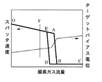
図1は、酸素ガスだけを導入した反応性スパッタによりTiOx膜を形成する場合の、スパッタ速度とターゲットセルフバイアス電位の変化を概念的に示した特性図である。図1において、実線は、スパッタ速度の変化を示し、点線は、ターゲットバイアス電圧の変化を示している。酸素ガス流量をゼロから増やしていくと、酸素ガス流量が低いうちはターゲット表面に金属Tiが露出しているため、いわゆるメタルモードのスパッタリングが進行する(O−A間)、このメタルモードにおいては、スパッタ速度も大きく、ターゲット電位も低い状態(マイナスの大きな値)にある。 FIG. 1 is a characteristic diagram conceptually showing changes in sputtering rate and target self-bias potential when a TiO x film is formed by reactive sputtering in which only oxygen gas is introduced. In FIG. 1, the solid line indicates the change in the sputtering rate, and the dotted line indicates the change in the target bias voltage. When the oxygen gas flow rate is increased from zero, so-called metal mode sputtering proceeds (between OA) because the metal Ti is exposed on the target surface while the oxygen gas flow rate is low. In this metal mode, The sputtering rate is high and the target potential is low (a large negative value).
これに対し、ターゲット表面がすべて酸化されると、ターゲット電位が急に上昇すると同時にスパッタ速度も1桁以上低下する(A→B)。この状態よりさらに酸素ガス流量を増やしても、スパッタ速度にあまり変化はない(B−C間)。この状態が、いわゆる酸化物モードのスパッタである。この状態より逆に、供給する酸素ガス流量を減らしていくと、今度は、C→D→E→Oのラインに沿ってスパッタ速度が変わる。このように、酸素ガスだけを用いた反応性スパッタによるTiOx膜の形成では、酸素ガス流量を増やしたときと減らしたときでは、図1に示すようなヒステリシスが生じる。 On the other hand, when the entire target surface is oxidized, the target potential rises rapidly, and at the same time, the sputtering rate decreases by one digit or more (A → B). Even if the oxygen gas flow rate is further increased from this state, the sputtering rate does not change much (between B and C). This state is so-called oxide mode sputtering. On the contrary, if the flow rate of the supplied oxygen gas is decreased, the sputtering rate changes along the line C → D → E → O. Thus, in the formation of the TiO x film by reactive sputtering using only oxygen gas, hysteresis as shown in FIG. 1 occurs when the oxygen gas flow rate is increased and decreased.
本実施の形態における透明導電膜の形成方法では、上述した酸素流量を変化させる中の遷移領域を避け、図1中のEの状態よりも左側のメタルモードの状態で、TiONの成膜を行うところに特徴がある。言い換えると、酸素ガスの供給流量を、ターゲットの表面に金属Tiが露出した状態が定常的に保持される上限の流量よりも少ない流量とし、上述した反応性スパッタによりTiONの成膜を行えばよい。 In the method for forming a transparent conductive film in the present embodiment, TiON film formation is performed in the metal mode state on the left side of the state E in FIG. 1 while avoiding the transition region in which the oxygen flow rate is changed as described above. There is a feature. In other words, the supply flow rate of oxygen gas may be set to a flow rate lower than the upper limit flow rate at which the state where metal Ti is exposed on the surface of the target is constantly maintained, and TiON film formation may be performed by the reactive sputtering described above. .
例えば、まず、TiONの形成に用いる反応性スパッタ装置において、図1を用いて説明したような酸素ガスの供給流量に対するスパッタ速度およびターゲットバイアス電圧の変化特性を取得しておき、メタルモードの酸素ガス流量の範囲を確定しておく。 For example, in the reactive sputtering apparatus used for forming TiON, first, the change characteristics of the sputtering rate and the target bias voltage with respect to the oxygen gas supply flow rate as described with reference to FIG. Determine the flow range.
次に、図1の例えばFの状態の酸素ガス流量において、窒素ガスも同時に導入してスパッタを行う。この場合、窒素ガス流量を増やしていくとスパッタ速度は緩やかに低下するものの、酸素ガス流量に対する変化ほど急激ではない。 Next, sputtering is performed by simultaneously introducing nitrogen gas at the oxygen gas flow rate in the state of F in FIG. 1, for example. In this case, the sputtering rate gradually decreases as the nitrogen gas flow rate is increased, but is not as rapid as the change with respect to the oxygen gas flow rate.
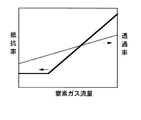
上述したことにより形成されるTiON膜の抵抗率と透過率を、窒素ガス流量に対してプロットすると、図2のようになる。図2において、実線は、形成されたTiON膜の抵抗率の変化を示し、点線は、透過率の変化を示している。窒素ガス流量が低い条件では、窒素ガス流量によらず抵抗率は一定である。これは酸素に結合していないTiの結合手に窒素原子が結合するためであり、透過率は向上するが、酸化度が変わらないため抵抗率はあまり影響を受けない。 The resistivity and transmittance of the TiON film formed as described above are plotted against the nitrogen gas flow rate as shown in FIG. In FIG. 2, the solid line shows the change in resistivity of the formed TiON film, and the dotted line shows the change in transmittance. Under the condition where the nitrogen gas flow rate is low, the resistivity is constant regardless of the nitrogen gas flow rate. This is because nitrogen atoms are bonded to Ti bonds that are not bonded to oxygen, and the transmittance is improved, but the resistivity is not significantly affected because the degree of oxidation does not change.
これに対し、窒素ガス流量をさらに増やしていくと、過剰に窒素原子が薄膜内に取り込まれるため、抵抗率は増大していくが、膜の透過率もより向上する。このように抵抗率と透過率とはトレードオフの関係にある。従って、より低抵抗なTiON膜が必要な場合には、多少透過率を犠牲にして、反応性スパッタにより成膜するときに供給する窒素ガス流量を低めに設定するとよい。これに対し、より高透過率なTiON膜が必要な場合には、供給する窒素ガスを多めに流せばよい。 On the other hand, when the nitrogen gas flow rate is further increased, excessive nitrogen atoms are taken into the thin film, so that the resistivity is increased, but the transmittance of the film is further improved. Thus, there is a trade-off relationship between resistivity and transmittance. Accordingly, when a TiON film having a lower resistance is required, the flow rate of nitrogen gas supplied when forming by reactive sputtering may be set lower, at the expense of some transmittance. On the other hand, when a TiON film having a higher transmittance is required, a larger amount of nitrogen gas may be supplied.
次に、金属Tiターゲットを用いた電子サイクロトロン共鳴(ECR)プラズマスパッタ法により、実際にガラス基板の上にTiON膜を形成した結果について説明する。ECRスパッタ法は、低ダメージ成膜を特徴とし、適切なガス流量の設定により低抵抗のZnO透明導電膜を形成できることが知られている。 Next, the results of actually forming a TiON film on a glass substrate by electron cyclotron resonance (ECR) plasma sputtering using a metal Ti target will be described. The ECR sputtering method is characterized by low damage film formation, and it is known that a low resistance ZnO transparent conductive film can be formed by setting an appropriate gas flow rate.
まず、本実施の形態におけるECRプラズマスパッタ法によるTiON膜の形成では、供給する酸素ガス流量に対して定常的にメタルモードが保たれる酸素ガス流量は、1.2sccm以下であった。なお、sccmは流量の単位であり、0℃・1気圧の流体が1分間に1cm3流れることを示す。 First, in the formation of the TiON film by the ECR plasma sputtering method in this embodiment, the oxygen gas flow rate at which the metal mode is constantly maintained with respect to the supplied oxygen gas flow rate is 1.2 sccm or less. Note that sccm is a unit of flow rate, and indicates that a fluid at 0 ° C. and 1 atm flows 1 cm 3 per minute.
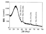
次に、形成したTiON膜の典型的なX線回折パタンを図3に示す。成膜の条件は、酸素ガス流量0.3sccm、窒素ガス流量0.6sccmである。この条件で形成したTiON膜は、抵抗率が0.63mΩcmであった。基板温度は室温(23℃程度)であるが、400℃においても同様なX線回折パタンが得られた。図3からわかるように、本実施の形態の形成法によるTiON膜は、面心立方格子構造のTiOやTiNの回折角とほぼ一致した位置に、(200)、(220)、(311)などのピークが見られる。このことから、TiONはTiOやTiNの面心立方格子構造と同じ構造を取ることが分かる。なお、この状態は、形成した膜中に、複数のTiONの微結晶粒が分散している状態と考えることができる。 Next, a typical X-ray diffraction pattern of the formed TiON film is shown in FIG. The film forming conditions are an oxygen gas flow rate of 0.3 sccm and a nitrogen gas flow rate of 0.6 sccm. The TiON film formed under these conditions had a resistivity of 0.63 mΩcm. The substrate temperature was room temperature (about 23 ° C.), but a similar X-ray diffraction pattern was obtained even at 400 ° C. As can be seen from FIG. 3, the TiON film formed by the formation method of the present embodiment has (200), (220), (311), etc. at positions substantially coincident with the diffraction angles of TiO and TiN having a face-centered cubic lattice structure. The peak is seen. This indicates that TiON has the same structure as the face-centered cubic lattice structure of TiO and TiN. This state can be considered as a state in which a plurality of fine crystal grains of TiON are dispersed in the formed film.
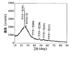
一方、酸素ガス流量0.6sccm、窒素ガス流量0.8sccmと、Tiが十分に酸化された状態になる条件でスパッタした膜のX線回折パタンを図4に示す。なお、成膜時の基板温度は450℃としている。図4に示すように、アナターゼ相に対応する回折ピーク(101),(004),(200),(105),(213)、および、ルチル相に対応する回折ピーク(110)が見られる。結晶構造がアナターゼ相のTiO2に近いことから、組成はTiO2-xNx(x〜2)であり、窒素原子は、アナターゼ相の結晶構造にあまり影響しないような格子間位置に入っていると推測される。この試料の抵抗率は、2.6Ωcmと高く、透明導電膜としての利用には向いていない。 On the other hand, FIG. 4 shows an X-ray diffraction pattern of a sputtered film under conditions where the oxygen gas flow rate is 0.6 sccm and the nitrogen gas flow rate is 0.8 sccm, and Ti is sufficiently oxidized. Note that the substrate temperature during film formation is 450 ° C. As shown in FIG. 4, diffraction peaks (101), (004), (200), (105), (213) corresponding to the anatase phase and a diffraction peak (110) corresponding to the rutile phase are observed. Since the crystal structure is close to TiO 2 in the anatase phase, the composition is TiO 2−x N x (x˜2), and the nitrogen atoms enter interstitial positions that do not significantly affect the crystal structure of the anatase phase. It is estimated that This sample has a high resistivity of 2.6 Ωcm and is not suitable for use as a transparent conductive film.
以上の結果から、Tiの酸化度がTiOに近い場合とTiO2に近い場合では、結晶構造が全く異なることがわかる。透明導電膜に適しているのは、前者の「Tiの酸化度がTiOに近い場合」である。よって、透明導電膜への適応性は、X線回折パタンにより判断することができる。 From the above results, it can be seen that the crystal structure is completely different when the oxidation degree of Ti is close to TiO and when it is close to TiO 2 . The former “when the oxidation degree of Ti is close to TiO” is suitable for the transparent conductive film. Therefore, the adaptability to the transparent conductive film can be determined by the X-ray diffraction pattern.
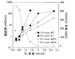
酸素ガス流量は、0.2sccmおよび0.3sccm、基板温度は、室温(RT)および400℃の各々の条件について、窒素ガス流量を変えたときの抵抗率を図5に示す。図5において、黒丸は、酸素ガス流量0.2sccm、基板温度は室温である。また、黒四角は、酸素ガス流量0.3sccm、基板温度は室温である。また、白丸は、酸素ガス流量0.3sccm、基板温度は400℃である。また、白四角は、酸素ガス流量0.3sccm、基板温度は400℃である。なお、白三角は、酸素ガス流量0.2sccm、基板温度を室温としたときの(200)回折ピーク強度の変化を示している。 FIG. 5 shows the resistivity when the nitrogen gas flow rate is changed under the conditions that the oxygen gas flow rate is 0.2 sccm and 0.3 sccm, the substrate temperature is room temperature (RT), and 400 ° C. In FIG. 5, black circles indicate an oxygen gas flow rate of 0.2 sccm, and the substrate temperature is room temperature. Further, the black squares represent an oxygen gas flow rate of 0.3 sccm and the substrate temperature is room temperature. White circles indicate an oxygen gas flow rate of 0.3 sccm and a substrate temperature of 400.degree. In the white square, the oxygen gas flow rate is 0.3 sccm, and the substrate temperature is 400 ° C. The white triangle indicates the change in (200) diffraction peak intensity when the oxygen gas flow rate is 0.2 sccm and the substrate temperature is room temperature.
黒丸、黒四角、白丸、および白四角の全般に、窒素ガス流量の増大に伴って高抵抗化している。室温での成膜(黒丸、黒四角)と400℃での成膜(白丸、白四角)とを比較すると、400℃での成膜の方がより低い抵抗率を示している。これは、高い温度でより結晶化が進んだ状態となり、この結晶化により電子の移動度が大きくなるためである。 The black circles, black squares, white circles, and white squares generally increase in resistance as the nitrogen gas flow rate increases. When film formation at room temperature (black circles, black squares) and film formation at 400 ° C. (white circles, white squares) are compared, the film formation at 400 ° C. shows a lower resistivity. This is because crystallization becomes more advanced at a high temperature, and the mobility of electrons increases due to this crystallization.
また、図5の白三角に示すように、窒素ガス流量を増やすと回折ピーク強度は減少し、形成される膜は、非晶質状態に近くなっている。窒素ガス流量1.5sccmまでは有為の回折ピーク強度があるが、これよりさらに高窒素ガス流量においては、非晶質である。 Further, as shown by the white triangles in FIG. 5, when the nitrogen gas flow rate is increased, the diffraction peak intensity decreases, and the formed film is close to an amorphous state. There is a significant diffraction peak intensity up to a nitrogen gas flow rate of 1.5 sccm, but it is amorphous at higher nitrogen gas flow rates.
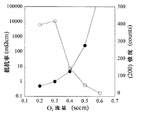
一方、窒素ガス流量0.8sccmにおいて、酸素ガス流量を変えたときの抵抗率の変化を図6に示す。図6において、白丸は、形成したTiON膜の抵抗率の変化を示し、黒丸は、(200)回折ピーク強度の変化を示している。酸素流量においては、この流量を増やすと急激に抵抗率が増大している。このことは、図5の結果も合わせ、酸素原子および窒素原子ともに、TiON膜内に過剰に取り込まれると高抵抗化することを示している。なお、図6に示すように、酸素ガス流量においては、わずかに0.3sccmの酸素ガス流量の変化で抵抗率が2桁変わるが、図5に示すように、窒素ガス流量においては、同様の抵抗変化を起こすためには、1sccmの窒素ガス流量変化を要している。このように、TiON膜においては、窒素よりも酸素の方が抵抗を高める効果がはるかに大きい。 On the other hand, FIG. 6 shows the change in resistivity when the oxygen gas flow rate is changed at a nitrogen gas flow rate of 0.8 sccm. In FIG. 6, white circles indicate changes in resistivity of the formed TiON film, and black circles indicate changes in (200) diffraction peak intensity. In the oxygen flow rate, when this flow rate is increased, the resistivity rapidly increases. This also shows that, together with the result of FIG. 5, when both oxygen atoms and nitrogen atoms are excessively taken into the TiON film, the resistance is increased. As shown in FIG. 6, in the oxygen gas flow rate, the resistivity changes by two orders of magnitude by a slight change in the oxygen gas flow rate of 0.3 sccm, but as shown in FIG. In order to cause a resistance change, a nitrogen gas flow rate change of 1 sccm is required. Thus, in the TiON film, the effect of increasing the resistance of oxygen is much greater than that of nitrogen.
また、図5に示す結果では、抵抗率が測定できる範囲に留まっているが、図6に示す結果では、酸素ガス流量0.6sccmの場合は、抵抗率はグラフの縦軸の範囲を大きくはみ出している。また酸素ガス流量0.5sccmまでは(200)回折ピークが何とか確認できるが、これ以上では観測されず、結晶になっていない。 In addition, in the result shown in FIG. 5, the resistivity remains within the measurable range. However, in the result shown in FIG. 6, when the oxygen gas flow rate is 0.6 sccm, the resistivity greatly exceeds the range of the vertical axis of the graph. ing. Further, although the (200) diffraction peak can be confirmed somehow up to an oxygen gas flow rate of 0.5 sccm, it is not observed beyond this and is not a crystal.
以上の図5および図6に示す結果より、TiON膜の抵抗率が透明導電膜として使える範囲に入るには、これが結晶となっていることを示す、面心立方格子構造の(200)回折ピークが出現することが必要条件とすることができる。 From the results shown in FIG. 5 and FIG. 6, the (200) diffraction peak of the face-centered cubic lattice structure indicates that the TiON film has a crystal in order to enter the range where the resistivity of the TiON film can be used as a transparent conductive film. Can be a prerequisite.
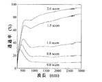
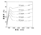
次に、金属Tiターゲットを用いたECRプラズマスパッタ法によるTiON膜の形成において、酸素ガス流量0.3sccmの条件の下、窒素ガス流量を変えて成膜したTiON膜の透過率の変化について図7および図8を用いて説明する。図7は、基板温度を室温としたときの、窒素ガス流量と形成されるTiON膜の透過率の変化との関係を示す特性図である。また、図8は、基板温度を400℃としたときの、窒素ガス流量と形成されるTiON膜の透過率の変化との関係を示す特性である。 Next, in the formation of a TiON film by ECR plasma sputtering using a metal Ti target, the change in transmittance of the TiON film formed by changing the nitrogen gas flow rate under the condition of the oxygen gas flow rate of 0.3 sccm is shown in FIG. This will be described with reference to FIG. FIG. 7 is a characteristic diagram showing the relationship between the nitrogen gas flow rate and the change in transmittance of the formed TiON film when the substrate temperature is room temperature. FIG. 8 is a characteristic showing the relationship between the flow rate of nitrogen gas and the change in transmittance of the formed TiON film when the substrate temperature is 400 ° C.
図7および図8に示すように、どちらの基板温度条件においても、窒素ガス流量の増大に伴って透過率は増大している。 As shown in FIGS. 7 and 8, the transmittance increases with an increase in the nitrogen gas flow rate in both substrate temperature conditions.
ここで、基板温度条件が、室温と400℃との結果を比較する。室温での成膜の場合、窒素ガス流量1.0sccmのとき、波長400〜800nmの可視光域の平均透過率は、40%であり、このとき抵抗率は4mΩcmである。窒素ガス流量1.5sccmのとき、可視域の平均透過率は60%であり、抵抗率は0.2Ωcmである。一方、400℃成膜の場合、窒素ガス流量1.0sccmのとき、平均透過率は50%であり、抵抗率は2.3mΩcmである。また、窒素ガス流量1.5sccmのとき、可視域の平均透過率は57%であり、抵抗率は6mΩcmである。これらのことより明らかに、同じガス流量であれば、室温成膜よりも400℃成膜の方が透過率はより高く、抵抗率はより低い。 Here, the substrate temperature condition is compared between room temperature and 400 ° C. In the case of film formation at room temperature, when the nitrogen gas flow rate is 1.0 sccm, the average transmittance in the visible light region having a wavelength of 400 to 800 nm is 40%, and the resistivity is 4 mΩcm. When the nitrogen gas flow rate is 1.5 sccm, the average transmittance in the visible region is 60%, and the resistivity is 0.2 Ωcm. On the other hand, in the case of forming a film at 400 ° C., when the nitrogen gas flow rate is 1.0 sccm, the average transmittance is 50% and the resistivity is 2.3 mΩcm. When the nitrogen gas flow rate is 1.5 sccm, the average transmittance in the visible region is 57% and the resistivity is 6 mΩcm. Obviously, at the same gas flow rate, the film formation at 400 ° C. has a higher transmittance and the resistivity is lower than the film formation at room temperature.
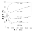
なお、金属Tiターゲットを用いたECRプラズマスパッタ法によるTiON膜の形成において、窒素ガス流量0.8sccmと同一条件とし、酸素ガス流量を0.2sccmから0.6sccmまで変化させたときの透過率の変化を図9に示す。この場合もやはり酸素ガス流量の増大とともに、TiON膜の透過率は増大している。ただし、前述したように、酸素ガス流量が大きい条件で形成したTiON膜の抵抗率は、高いものとなり、導電膜には適していないものとなる。 In the formation of a TiON film by an ECR plasma sputtering method using a metallic Ti target, the transmittance is the same when the nitrogen gas flow rate is the same as 0.8 sccm and the oxygen gas flow rate is changed from 0.2 sccm to 0.6 sccm. The change is shown in FIG. In this case as well, the transmittance of the TiON film increases as the oxygen gas flow rate increases. However, as described above, the resistivity of the TiON film formed under a condition where the oxygen gas flow rate is large is high and is not suitable for the conductive film.
以上に説明したように、金属Tiターゲットを用いた反応性スパッタ法で、酸素ガスの流量を、ターゲットの表面に金属Tiが露出した状態が定常的に保持される上限の流量よりも少ない流量とする条件としてTiON膜を形成することで、TiOxやTiNよりも透過率が高く、TiO2よりも抵抗率の低い透明導電膜TiONを得ることができる。 As described above, in the reactive sputtering method using a metal Ti target, the flow rate of oxygen gas is smaller than the upper limit flow rate at which the state where the metal Ti is exposed on the surface of the target is constantly maintained. By forming a TiON film as a condition for this, it is possible to obtain a transparent conductive film TiON having a higher transmittance than TiO x and TiN and a lower resistivity than TiO 2 .
TiONは、ZnやInよりもクラーク数が大きなTiという、地球上に豊富に存在する元素を主成分としている。また、Nbのような希少金属のドーピング材料を使用していない。従って、ITO、ZnO系透明導電膜、およびNbドープTiO2などに比較し、本発明の透明導電膜は、環境適合性が高く、低コストで形成することができる。また、成膜時の基板温度条件を室温程度としていても、相応の透明性および導電性を発現することができるため、ZnO系とは別系列の透明導電膜として使用することができる。 TiON is mainly composed of an element abundant on the earth called Ti, which has a larger Clark number than Zn and In. Further, a rare metal doping material such as Nb is not used. Accordingly, the transparent conductive film of the present invention has higher environmental compatibility and can be formed at lower cost than ITO, ZnO-based transparent conductive film, Nb-doped TiO 2 and the like. Further, even if the substrate temperature condition during film formation is about room temperature, it can exhibit appropriate transparency and conductivity, and therefore can be used as a transparent conductive film of a different series from the ZnO system.
Claims (5)
前記結晶は、面心立方格子構造のTiOもしくはTiNの回折点(200)と同じ位置にX線の回折ピークを示す結晶性を有することを特徴とする透明導電膜。 The transparent conductive film according to claim 1,
The transparent conductive film characterized in that the crystal has crystallinity showing an X-ray diffraction peak at the same position as a diffraction point (200) of TiO or TiN having a face-centered cubic lattice structure.
前記酸素ガスの流量は、前記ターゲットの表面に金属Tiが露出した状態が定常的に保持される上限の流量よりも少ない流量とする
ことを特徴とする透明導電膜の形成方法。 A plasma composed of an inert gas, an oxygen gas, and a nitrogen gas is generated, a negative bias is applied to a target composed of metal Ti, and particles generated from the plasma collide with the target to cause a sputtering phenomenon, Depositing a material constituting the target on a substrate to form a transparent conductive film composed of TiON crystals on the substrate;
The method for forming a transparent conductive film is characterized in that the flow rate of the oxygen gas is lower than an upper limit flow rate at which the state where the metal Ti is exposed on the surface of the target is constantly maintained.
前記透明導電膜の形成は、前記基板を加熱しながら行うことを特徴とする透明導電膜の形成方法。 In the formation method of the transparent conductive film of Claim 3,
The formation of the transparent conductive film is performed while heating the substrate.
前記プラズマは、電子サイクロトロン共鳴により生成されて発散磁界により運動エネルギーが与えられた電子サイクロトロン共鳴プラズマであることを特徴とする透明導電膜の形成方法。 In the formation method of the transparent conductive film of Claim 3,
The method of forming a transparent conductive film, wherein the plasma is electron cyclotron resonance plasma generated by electron cyclotron resonance and given kinetic energy by a divergent magnetic field.
Priority Applications (1)
| Application Number | Priority Date | Filing Date | Title |
|---|---|---|---|
| JP2009166999A JP2011021237A (en) | 2009-07-15 | 2009-07-15 | Transparent conductive film and method for forming the same |
Applications Claiming Priority (1)
| Application Number | Priority Date | Filing Date | Title |
|---|---|---|---|
| JP2009166999A JP2011021237A (en) | 2009-07-15 | 2009-07-15 | Transparent conductive film and method for forming the same |
Publications (1)
| Publication Number | Publication Date |
|---|---|
| JP2011021237A true JP2011021237A (en) | 2011-02-03 |
Family
ID=43631553
Family Applications (1)
| Application Number | Title | Priority Date | Filing Date |
|---|---|---|---|
| JP2009166999A Pending JP2011021237A (en) | 2009-07-15 | 2009-07-15 | Transparent conductive film and method for forming the same |
Country Status (1)
| Country | Link |
|---|---|
| JP (1) | JP2011021237A (en) |
Cited By (3)
| Publication number | Priority date | Publication date | Assignee | Title |
|---|---|---|---|---|
| JP2013014832A (en) * | 2011-07-06 | 2013-01-24 | Toyota Central R&D Labs Inc | Transparent conductive film, conductive member and method for producing the same |
| JP2016194110A (en) * | 2015-03-31 | 2016-11-17 | デクセリアルズ株式会社 | Production of multilayer film structure |
| WO2022038676A1 (en) * | 2020-08-18 | 2022-02-24 | 日本電信電話株式会社 | Amorphous semiconductor thin film |
Citations (4)
| Publication number | Priority date | Publication date | Assignee | Title |
|---|---|---|---|---|
| JPH0610125A (en) * | 1992-06-26 | 1994-01-18 | Sony Corp | Thin film formation method |
| JP2000294738A (en) * | 1999-04-08 | 2000-10-20 | Nec Corp | Thin film resistor and manufacturing method thereof |
| JP2003231966A (en) * | 2002-02-08 | 2003-08-19 | Central Glass Co Ltd | Process for forming titanium oxide film |
| JP2008229419A (en) * | 2007-03-16 | 2008-10-02 | Bridgestone Corp | Photocatalytic nitrogen-doped titanium oxide thin film and its depositing method |
-
2009
- 2009-07-15 JP JP2009166999A patent/JP2011021237A/en active Pending
Patent Citations (4)
| Publication number | Priority date | Publication date | Assignee | Title |
|---|---|---|---|---|
| JPH0610125A (en) * | 1992-06-26 | 1994-01-18 | Sony Corp | Thin film formation method |
| JP2000294738A (en) * | 1999-04-08 | 2000-10-20 | Nec Corp | Thin film resistor and manufacturing method thereof |
| JP2003231966A (en) * | 2002-02-08 | 2003-08-19 | Central Glass Co Ltd | Process for forming titanium oxide film |
| JP2008229419A (en) * | 2007-03-16 | 2008-10-02 | Bridgestone Corp | Photocatalytic nitrogen-doped titanium oxide thin film and its depositing method |
Non-Patent Citations (1)
| Title |
|---|
| JPN6013007492; A. Armigliato, et al.: 'Characterization of titanium nitride films deposited onto silicon' Thin Solid Films Volume 92, Issue 4, 1982, Pages 341-346 * |
Cited By (3)
| Publication number | Priority date | Publication date | Assignee | Title |
|---|---|---|---|---|
| JP2013014832A (en) * | 2011-07-06 | 2013-01-24 | Toyota Central R&D Labs Inc | Transparent conductive film, conductive member and method for producing the same |
| JP2016194110A (en) * | 2015-03-31 | 2016-11-17 | デクセリアルズ株式会社 | Production of multilayer film structure |
| WO2022038676A1 (en) * | 2020-08-18 | 2022-02-24 | 日本電信電話株式会社 | Amorphous semiconductor thin film |
Similar Documents
| Publication | Publication Date | Title |
|---|---|---|
| CN101910450B (en) | Preparation method of a-IGZO oxide film | |
| TWI532862B (en) | A sputtering target, a method for forming an amorphous oxide film using the same, and a method for manufacturing a thin film transistor | |
| Bitla et al. | Oxide heteroepitaxy for flexible optoelectronics | |
| JP5376750B2 (en) | Semiconductor thin film, manufacturing method thereof, thin film transistor, active matrix drive display panel | |
| JP5005772B2 (en) | Conductive laminate and manufacturing method thereof | |
| CN107074662B (en) | Metal oxide thin film, method for depositing metal oxide thin film, and apparatus including metal oxide thin film | |
| JP5492479B2 (en) | Method for producing transparent conductive film | |
| JP2010070409A (en) | Method for producing oxide sintered compact | |
| KR20200029109A (en) | Composition for Sputtering Target for Thin Film and Method for Making Sputtering Target | |
| CN102666429B (en) | Indium oxide sintered body and indium oxide transparent conductive film | |
| US8062777B2 (en) | Semiconductor thin film and process for producing the same | |
| JPH06290641A (en) | Noncrystal transparent conductive membrane | |
| JP2011021237A (en) | Transparent conductive film and method for forming the same | |
| JP5243459B2 (en) | Method for forming transparent conductive film | |
| CN101997081A (en) | Resistive random access memory and preparation method thereof | |
| Yamada et al. | Enhanced carrier transport in uniaxially (001)-oriented anatase Ti0. 94Nb0. 06O2 films grown on nanosheet seed layers | |
| Kuppan et al. | Structural, optical and magnetic properties of Ni-doped SnO2 thin films prepared by flash evaporation technique | |
| JP4370868B2 (en) | Oxide sintered body, sputtering target, and method for producing oxide transparent electrode film | |
| JP5702447B2 (en) | Semiconductor thin film, manufacturing method thereof, and thin film transistor | |
| Cho et al. | Effect of Ga doping concentrations, substrate temperatures and working pressures on the electrical and optical properties of ZnO thin films | |
| CN101104548A (en) | A kind of indium-aluminum co-doped low-resistance P-type tin dioxide film material and its manufacturing method | |
| Balada et al. | Influence of an Al‐Doped ZnO Interface Layer on the Thermochromic Properties of VO2 Thin Films Deposited by RF Magnetron Sputtering | |
| JP2011179021A (en) | Conductor and method for manufacturing conductor | |
| KR20110111230A (en) | Transparent electrode material, manufacturing method thereof and manufacturing method of transparent electrode | |
| JP5678149B2 (en) | Semiconductor thin film, manufacturing method thereof, thin film transistor, active matrix drive display panel |
Legal Events
| Date | Code | Title | Description |
|---|---|---|---|
| RD02 | Notification of acceptance of power of attorney |
Free format text: JAPANESE INTERMEDIATE CODE: A7422 Effective date: 20111108 |
|
| RD04 | Notification of resignation of power of attorney |
Free format text: JAPANESE INTERMEDIATE CODE: A7424 Effective date: 20111108 |
|
| A621 | Written request for application examination |
Free format text: JAPANESE INTERMEDIATE CODE: A621 Effective date: 20111121 |
|
| A977 | Report on retrieval |
Free format text: JAPANESE INTERMEDIATE CODE: A971007 Effective date: 20130213 |
|
| A131 | Notification of reasons for refusal |
Free format text: JAPANESE INTERMEDIATE CODE: A131 Effective date: 20130226 |
|
| A02 | Decision of refusal |
Free format text: JAPANESE INTERMEDIATE CODE: A02 Effective date: 20130709 |