JP2011040468A - Antireflection film for solid-state image pickup element - Google Patents
Antireflection film for solid-state image pickup element Download PDFInfo
- Publication number
- JP2011040468A JP2011040468A JP2009184495A JP2009184495A JP2011040468A JP 2011040468 A JP2011040468 A JP 2011040468A JP 2009184495 A JP2009184495 A JP 2009184495A JP 2009184495 A JP2009184495 A JP 2009184495A JP 2011040468 A JP2011040468 A JP 2011040468A
- Authority
- JP
- Japan
- Prior art keywords
- film
- layer
- light
- phase inversion
- antireflection
- Prior art date
- Legal status (The legal status is an assumption and is not a legal conclusion. Google has not performed a legal analysis and makes no representation as to the accuracy of the status listed.)
- Granted
Links
Images
Landscapes
- Solid State Image Pick-Up Elements (AREA)
- Surface Treatment Of Optical Elements (AREA)
Abstract
【課題】固体撮像素子の受光部以外の箇所に被膜される遮光用金属膜上に設けられる反射防止膜において、近赤外領域の光に対する反射防止効果を向上させる。
【解決手段】反射防止膜1は、遮光用金属膜3の上層にある位相反転用絶縁層4と、この位相反転用絶縁層4の上層にある表層金属層5と、表層金属層5の上層にある保護膜層6と、を備える。また、位相反転用絶縁層4は、その屈折率をn、対象波長の波長をλとしたときに、略λ/4nとなる膜厚に成膜され、表層金属層5は、シート抵抗が略100〜450Ω/□となる膜厚に成膜される。この構成によれば、遮光用金属膜3の表面に入射した光の一部を、位相反転用絶縁層4の表面と遮光用金属膜3の表面との間で、位相反転させながら繰り返し再反射させて消衰させることにより、高い反射防止効果を実現できる。
【選択図】図1An antireflection film provided on a light-shielding metal film coated on a portion other than a light receiving portion of a solid-state imaging device improves an antireflection effect on light in the near infrared region.
An antireflection film includes a phase inversion insulating layer overlying a light shielding metal film, a surface metal layer overlying the phase inversion insulating layer, and an upper layer of the surface metal layer. And a protective film layer 6. The phase inversion insulating layer 4 is formed to a thickness of approximately λ / 4n when the refractive index is n and the wavelength of the target wavelength is λ, and the surface metal layer 5 has a sheet resistance of approximately The film is formed to a thickness of 100 to 450Ω / □. According to this configuration, a part of light incident on the surface of the light shielding metal film 3 is repeatedly rereflected while being phase-inverted between the surface of the phase inversion insulating layer 4 and the surface of the light shielding metal film 3. By making them extinguish, a high antireflection effect can be realized.
[Selection] Figure 1
Description
本発明は、固体撮像素子の遮光用金属膜上に設けられる固体撮像素子用の反射防止膜に関する。 The present invention relates to an antireflection film for a solid-state image sensor provided on a light-shielding metal film of a solid-state image sensor.
従来から、対象となる空間に光を照射して、その光が反射して返ってくるまでの到達時間を画素毎に計測すると共に、それらの画像情報を重ねることで、対象となる画像と、その対象までの距離とを画素毎に出力する距離画像センサが知られている。一般に、この種の距離画像センサにおいては、人の目視等や通常の撮像に影響を与えないように、計測用の照射光として近赤外線が用いられる。 Conventionally, by irradiating the target space with light, measuring the arrival time until the light is reflected and returned for each pixel, and overlapping the image information, the target image, A distance image sensor that outputs the distance to the target for each pixel is known. In general, in this type of distance image sensor, near infrared rays are used as irradiation light for measurement so as not to affect human visual observation or normal imaging.
例えば、CCD撮像素子を用いた周囲光消去型の距離画像センサにおける撮像部は、複数の画素を構成する光電変換部(受光部)と、各画素の仕切りとなる周囲光消去機能領域とが設けられている。そして、この周囲光消去機能領域といった、受光部を除く所定箇所には遮光用金属膜が選択的に成膜されている。 For example, an imaging unit in an ambient light erasing type distance image sensor using a CCD imaging device includes a photoelectric conversion unit (light receiving unit) that constitutes a plurality of pixels and an ambient light erasing function region that serves as a partition for each pixel. It has been. A light-shielding metal film is selectively formed at a predetermined location excluding the light receiving portion, such as the ambient light erasing function region.
しかし、これら遮光用金属膜で反射した近赤外線は、パッケージ封止ガラスやレンズ等といった光学部材で再反射して、当該画素以外の画素の受光部に入射してしまい、各画素における距離情報の取得を阻害することがある。そのため、このような遮光用金属膜上には、所定波長の光の反射を防止するための反射防止膜が設けられている。例えば、特許文献1には、遮光用金属膜上に、窒化チタン(TiN)から成る反射防止膜を、その膜厚が25nm以上となるように形成した例が記載されている。
However, near-infrared rays reflected by these light-shielding metal films are reflected again by an optical member such as a package sealing glass and a lens, and enter a light-receiving portion of a pixel other than the pixel. May interfere with acquisition. Therefore, an antireflection film for preventing reflection of light having a predetermined wavelength is provided on such a light shielding metal film. For example,
しかしながら、上記特許文献1に記載された反射防止膜は、波長450〜550nmの入射光に対する相対反射率が50%以下であるが、長波長側へ向かうほど相対反射率が増加する。すなわち、長波長の光に対する反射防止効果が低下する。しかも、近赤外線領域、特に距離画像センサで頻用される短波長側の近赤外線領域(一般に波長750〜1100nm)においては、相対反射率が60%以上であり、距離画素センサ用の反射防止膜としては、その反射防止効果が十分でない。
However, the antireflection film described in
本発明は、上記課題を解決するものであり、距離画素センサ等に用いられる固体撮像素子の遮光用金属膜上に設けられ、所望の波長領域の光に対する反射率を効果的に低下させることができる反射防止膜を提供することを目的とする。 The present invention solves the above-described problems, and is provided on a light-shielding metal film of a solid-state imaging device used for a distance pixel sensor or the like, and can effectively reduce the reflectance with respect to light in a desired wavelength region. An object of the present invention is to provide an antireflection film that can be used.
上記課題を解決するため、請求項1の発明は、固体撮像素子の受光部以外の箇所に選択的に被膜される遮光用金属膜上に設けられる固体撮像素子用の反射防止膜であって、前記遮光用金属膜の上層に設けられる位相反転用絶縁層と、該位相反転用絶縁層の上層に設けられる表層金属層と、該表層金属層の上層に設けられる保護膜層と、を備え、前記位相反転用絶縁層は、その屈折率をn、対象波長の波長をλとしたときに、略λ/4nとなる膜厚に成膜され、前記表層金属層は、シート抵抗が略100〜450Ω/□となる膜厚に成膜されたものである。
In order to solve the above-mentioned problem, the invention of
請求項2の発明は、請求項1に記載の固体撮像素子用の反射防止膜において、前記表層金属層が窒化チタン又はチタンを含む材料から成るものである。 According to a second aspect of the present invention, in the antireflection film for a solid-state imaging device according to the first aspect, the surface metal layer is made of titanium nitride or a material containing titanium.
請求項3の発明は、請求項1又は請求項2に記載の固体撮像素子用の反射防止膜において、前記位相反転用絶縁層と前記遮光メタル層との間に、窒化チタンを含む材料から成る層を更に設けたものである。 According to a third aspect of the present invention, in the antireflection film for a solid-state imaging device according to the first or second aspect, the antireflection film for a solid-state imaging device is made of a material containing titanium nitride between the phase inversion insulating layer and the light shielding metal layer. A layer is further provided.
請求項4の発明は、請求項1乃至請求項3のいずれか一項に記載の固体撮像素子用の反射防止膜において、前記保護膜層の上層に、樹脂保護層を更に設けたものである。 According to a fourth aspect of the present invention, in the antireflection film for a solid-state imaging device according to any one of the first to third aspects, a resin protective layer is further provided on the protective film layer. .
請求項1及び請求項2の発明によれば、遮光用金属膜の表面に入射した光の一部を、位相反転用絶縁層の表面と遮光用金属膜の表面との間で、位相反転させながら繰り返し再反射させて消衰させることにより、高い反射防止効果を実現できる。 According to the first and second aspects of the present invention, a part of the light incident on the surface of the light shielding metal film is phase-inverted between the surface of the phase inversion insulating layer and the surface of the light shielding metal film. However, a high antireflection effect can be realized by repeatedly rereflecting and extinguishing.
請求項3の発明によれば、窒化チタンを含む材料から成る内層金属層に入射した光の一部が全反射し、位相反転用絶縁層に戻されるので、上述した再反射の繰り返しによる反射光の消衰効果を更に高めることができる。 According to the third aspect of the present invention, part of the light incident on the inner metal layer made of the material containing titanium nitride is totally reflected and returned to the phase inversion insulating layer. The extinction effect of can be further enhanced.
請求項4の発明によれば、アクリル保護層が設けられることにより、反射防止膜の膜強度が向上する。
According to invention of
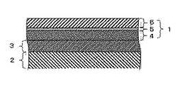
本発明の第1の実施形態に係る固体撮像素子用の反射防止膜(以下、反射防止膜1という)について、図1を参照して説明する。本実施形態の反射防止膜1は、固体撮像素子の受光部を除く箇所、ここではSiO2等から成る基材2上に、選択的に被膜される遮光用金属膜3上に設けられるものである。反射防止膜1は、上記遮光用金属膜3の上層に設けられる位相反転用絶縁層4と、この位相反転用絶縁層4の上層に設けられる表層金属層5と、この表層金属層5の上層に設けられる保護膜層6とを備える。
An antireflection film (hereinafter referred to as an antireflection film 1) for a solid-state imaging device according to a first embodiment of the present invention will be described with reference to FIG. The
遮光用金属膜3には、基材2との接着性が良く、反射率が高い金属材料、例えばアルミニウム(Al)等が用いられる。
The light
位相反転用絶縁層4は、その屈折率がn、対象波長の波長をλであるときに、略λ/4nとなる膜厚に成膜され、好ましくは、窒化シリコン(例えばSi3N4)又は酸化シリコン(例えばSiO2)等を含む透光性材料から形成されるものである。
The phase
表層金属層5は、シート抵抗が略100〜400Ω/□となる膜厚に成膜され、好ましくは、窒化チタン(TiN)又はチタン(Ti)を含む透光性材料から形成される。 The surface metal layer 5 is formed to a film thickness with a sheet resistance of approximately 100 to 400Ω / □, and is preferably formed from a light-transmitting material containing titanium nitride (TiN) or titanium (Ti).
保護膜層6は、成膜時における膜厚制御が可能であり、比較的屈折率が低い透光性材料であれば特に限定されないが、好ましくは、酸化シリコン等を含む透光性材料から形成される。表層金属層5は、光の透過率が確保されるように、位相反転用絶縁層4や遮光用金属膜3に比べて薄く形成されているので、耐久性が低い。そのため、保護膜層6が設けられることにより、物理的又は化学的ダメージから表層金属層5を保護することができる。
The protective film layer 6 is not particularly limited as long as the film thickness can be controlled at the time of film formation and is a light-transmitting material having a relatively low refractive index, but preferably formed from a light-transmitting material containing silicon oxide or the like. Is done. Since the surface metal layer 5 is formed thinner than the phase
本実施形態の反射防止膜1においては、位相反転用絶縁層4の上層に表層金属層5が設けられるので、遮光用金属膜3の表面で反射されて、位相反転用絶縁層4の表面(位相反転用絶縁層4と表層金属層5との界面)に入射した光の一部は、この界面で全反射し、遮光用金属膜3の表面に再入射する。すなわち、遮光用金属膜3の表面に入射した光の一部は、位相反転用絶縁層4の表面と遮光用金属膜3の表面との間で、位相反転しながら反射を繰り返す。このようにして、本実施形態の反射防止膜1は、位相反転用絶縁層4内で光を導波させて、これを消衰させることにより、反射防止効果を実現する。
In the
また、上述したように、位相反転用絶縁層4は、略λ/4nとなる膜厚に成膜されている。そのため、遮光用金属膜3の表面(位相反転用絶縁層4と遮光用金属膜3との界面)に入射した光は、位相反転用絶縁層4の表面(表層金属層5と位相反転用絶縁層4との界面)で反射した光に対して、位相が反転された状態で反射する。こうして、遮光用金属膜3の表面及び位相反転用絶縁層4の夫々の表面で反射した光が打ち消しあうことにより、一般の反射防止膜と同様の反射防止効果が実現される。すなわち、上述したように、位相反転用絶縁層4内で光を消衰させると共に、位相反転された光の打ち消しにより、より効果的な反射防止効果が得られる。
Further, as described above, the phase
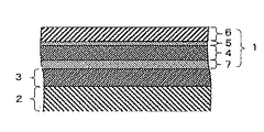
次に、本発明の第2の実施形態に係る反射防止膜について、図2を参照して説明する。本実施形態の反射防止膜1は、上述した第1の実施形態の反射防止膜1において、位相反転用絶縁層4と遮光金属膜3との間に、窒化チタンを含む材料から成る内層金属層7が更に設けられたものである。この内層金属層7の膜厚は、25nm以下であることが望ましい。この構成によれば、内層金属層7に入射した光の一部が全反射し、位相反転用絶縁層4に戻される。そのため、上述した再反射の繰り返しによる反射光の消衰効果を更に高めることができる。
Next, an antireflection film according to a second embodiment of the present invention will be described with reference to FIG. The
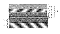
次に、本発明の第3の実施形態に係る反射防止膜について、図3を参照して説明する。本実施形態の反射防止膜1は、上述した第2の実施形態の反射防止膜1において、保護膜層6の上層に、樹脂保護層8が更に設けられたものである。樹脂保護層8としては、例えば、マイクロレンズ用のアクリル膜等が用いられる。この樹脂保護層8が設けられることにより、反射防止膜1の膜強度が向上する。なお、樹脂保護層8を構成する樹脂材料中に、例えば、染料等を添加して反射防止膜1に着色性を持たせてもよいし、紫外線吸収剤等を添加して、基材2等の外光による劣化を抑制できるようにしてもよい。
Next, an antireflection film according to a third embodiment of the present invention will be described with reference to FIG. The
以下、上述した第1〜第3の実施形態の夫々に対応する実施例1〜3について、比較例と対比して説明する。なお、これら実施例1〜3及び比較例は、近赤外領域にある波長870nmの光を反射防止の対象とする。 Hereinafter, Examples 1 to 3 corresponding to the first to third embodiments described above will be described in comparison with a comparative example. In addition, these Examples 1-3 and a comparative example make the light of wavelength 870nm in a near infrared region the object of antireflection.
(実施例1)
実施例1に係る反射防止膜1は、二酸化ケイ素(SiO2)等から成る基材2上に膜厚1μmのアルミニウムから成る遮光用金属膜3を形成しておき、この遮光用金属膜3上に形成される。より具体的には、この反射防止膜1は、位相反転用絶縁層4として膜厚110nmの窒化シリコン(SiN)から成る層(屈折率n=2.0)と、表層金属層5として膜厚10nm(シート抵抗200Ω/□に相当する)の窒化チタン(TiN)から成る層と、保護膜層6として膜厚400nmの酸化シリコン(SiO2)から成る層とが遮光用金属膜3上に積層されたものである。
Example 1
The
(実施例2)
実施例2に係る反射防止膜1は、位相反転用絶縁層4と遮光金属膜3との間に、内層金属層7として、膜厚15nmのTiNを設けた点が上記実施例1と異なる。
(Example 2)
The
(実施例3)
実施例2に係る反射防止膜1は、保護膜層6上に、樹脂保護層8として、マイクロレンズ用樹脂膜を3μm形成した点が上記実施例2と異なる。
(Example 3)
The
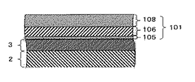
(比較例)
比較例に係る反射防止膜101の構成を図4に示す。反射防止膜101は、位相反転用絶縁層4が設けられておらず、表層金属層105として膜厚100nmの窒化チタン(TiN)から成る層と、保護膜層106として膜厚400nmの酸化シリコン(SiO2)から成る層と、樹脂保護層108として膜厚3μmの樹脂膜とが遮光用金属層3上に積層されたものである。他の構成は、実施例1と同様である。
(Comparative example)
The configuration of the
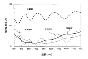
図5は、上述した実施例1〜3及び比較例における相対反射率のスペクトルを示す。これら相対反射率は、表層金属層105の膜厚が15nmである例(従来構造の反射防止膜(図4参照))の反射率を100%とした場合の相対反射率を示す。比較例に係る反射防止膜は、波長900nmの光における相対反射率が約70%であった。すなわち、特許文献1(特開2000−294755号公報)に示されるような、遮光金属膜上に形成される表層金属層(TiN)の膜厚を25nm以上にした場合であっても、波長900nmの光に対する反射防止効率はあまり向上しないことが示された。これに対して、実施例1に係る反射防止膜は、波長900nmの光における相対反射率が約8%であり、比較例に比べて反射防止効率が大幅に向上した。
FIG. 5 shows the spectrum of relative reflectance in Examples 1 to 3 and the comparative example described above. These relative reflectivities indicate relative reflectivities when the reflectivity of an example in which the thickness of the
また、実施例2に係る反射防止膜1は、波長900nmの光における相対反射率は約6%であり、比較例に対して反射防止効率が向上した。この実施例2は、実施例1に比べて、波長略900nm以上の相対的に長波長側の光の反射防止効果に優れていた。
Further, the
実施例3に係る反射防止膜1は、波長900nmの光における相対反射率は約8%であり、比較例に対して反射防止効率が向上した。この実施例3は、波長によって相対反射率がやや低くなる領域と、やや高くなる領域とがあり、その反射防止特性として波長依存性を有するものの、概して実施例1,2と同等の反射防止効果を有するものであった。
The
上記実施例1〜3は、いずれも波長900nmの光における相対反射率が10%以下であり、比較例に比べて優れた反射防止効果を示した。また、波長750n〜1100nmの光に対しても優れた反射防止効果を示した。これらの結果は、近赤外線を用いて距離情報を取得する固体撮像素子にとって、好適な反射防止膜を実現するものである。ただし、上述した反射防止膜1は、固体撮像素子以外の用途に対しても当然に適用し得るものである。なお、本発明は、位相反転用絶縁層4の表面と遮光用金属膜3の表面との間で、再反射を繰り返させてこれを消衰させるよう構成されたものであれば、必ずしも上述の実施形態に示す構成に限られるものではない。
In each of Examples 1 to 3, the relative reflectance in light having a wavelength of 900 nm was 10% or less, and an antireflection effect superior to that of the comparative example was exhibited. Moreover, the antireflection effect which was excellent also with respect to the light of wavelength 750n-1100nm was shown. These results realize an antireflection film suitable for a solid-state imaging device that acquires distance information using near infrared rays. However, the above-described
1 反射防止膜
2 基材
3 遮光用金属膜
4 位相反転用絶縁層
5 表層金属層
6 保護膜層
7 内層金属層
8 樹脂保護層
DESCRIPTION OF
Claims (4)
前記遮光用金属膜の上層に設けられる位相反転用絶縁層と、該位相反転用絶縁層の上層に設けられる表層金属層と、該表層金属層の上層に設けられる保護膜層と、を備え、
前記位相反転用絶縁層は、その屈折率をn、対象波長の波長をλとしたときに、略λ/4nとなる膜厚に成膜され、
前記表層金属層は、シート抵抗が略100〜450Ω/□となる膜厚に成膜されたことを特徴とする固体撮像素子用の反射防止膜。 An antireflection film for a solid-state image sensor provided on a light-shielding metal film that is selectively coated on a portion other than the light receiving portion of the solid-state image sensor,
An insulating layer for phase inversion provided on an upper layer of the light shielding metal film, a surface metal layer provided on an upper layer of the insulating layer for phase inversion, and a protective film layer provided on an upper layer of the surface metal layer,
The insulating layer for phase inversion is formed to a film thickness of approximately λ / 4n, where n is the refractive index and λ is the wavelength of the target wavelength.
The antireflection film for a solid-state imaging device, wherein the surface metal layer is formed to a film thickness with a sheet resistance of about 100 to 450 Ω / □.
Priority Applications (1)
| Application Number | Priority Date | Filing Date | Title |
|---|---|---|---|
| JP2009184495A JP5413040B2 (en) | 2009-08-07 | 2009-08-07 | Antireflection film for solid-state image sensor |
Applications Claiming Priority (1)
| Application Number | Priority Date | Filing Date | Title |
|---|---|---|---|
| JP2009184495A JP5413040B2 (en) | 2009-08-07 | 2009-08-07 | Antireflection film for solid-state image sensor |
Publications (2)
| Publication Number | Publication Date |
|---|---|
| JP2011040468A true JP2011040468A (en) | 2011-02-24 |
| JP5413040B2 JP5413040B2 (en) | 2014-02-12 |
Family
ID=43767965
Family Applications (1)
| Application Number | Title | Priority Date | Filing Date |
|---|---|---|---|
| JP2009184495A Expired - Fee Related JP5413040B2 (en) | 2009-08-07 | 2009-08-07 | Antireflection film for solid-state image sensor |
Country Status (1)
| Country | Link |
|---|---|
| JP (1) | JP5413040B2 (en) |
Cited By (1)
| Publication number | Priority date | Publication date | Assignee | Title |
|---|---|---|---|---|
| WO2021059850A1 (en) * | 2019-09-27 | 2021-04-01 | 三井化学株式会社 | Light-transmitting member and method for producing lens and light-transmitting member |
Families Citing this family (1)
| Publication number | Priority date | Publication date | Assignee | Title |
|---|---|---|---|---|
| IT201800009060A1 (en) | 2018-10-01 | 2020-04-01 | Salvagnini Italia Spa | HYDRAULIC DRIVE SYSTEM FOR A PUNCHING APPARATUS |
Citations (5)
| Publication number | Priority date | Publication date | Assignee | Title |
|---|---|---|---|---|
| JPH04199876A (en) * | 1990-11-29 | 1992-07-21 | Nec Corp | Solid state image sensing device and manufacture thereof |
| JPH06342896A (en) * | 1993-06-01 | 1994-12-13 | Matsushita Electron Corp | Solid-state image sensor and manufacture thereof |
| JPH10223871A (en) * | 1997-02-07 | 1998-08-21 | Denso Corp | Integrated optical sensor |
| JP2000298062A (en) * | 1999-04-14 | 2000-10-24 | Nec Corp | Thermal type functional device, energy detection device, and method of driving thermal type functional device |
| JP2007305675A (en) * | 2006-05-09 | 2007-11-22 | Sony Corp | Solid-state imaging device, imaging device |
-
2009
- 2009-08-07 JP JP2009184495A patent/JP5413040B2/en not_active Expired - Fee Related
Patent Citations (5)
| Publication number | Priority date | Publication date | Assignee | Title |
|---|---|---|---|---|
| JPH04199876A (en) * | 1990-11-29 | 1992-07-21 | Nec Corp | Solid state image sensing device and manufacture thereof |
| JPH06342896A (en) * | 1993-06-01 | 1994-12-13 | Matsushita Electron Corp | Solid-state image sensor and manufacture thereof |
| JPH10223871A (en) * | 1997-02-07 | 1998-08-21 | Denso Corp | Integrated optical sensor |
| JP2000298062A (en) * | 1999-04-14 | 2000-10-24 | Nec Corp | Thermal type functional device, energy detection device, and method of driving thermal type functional device |
| JP2007305675A (en) * | 2006-05-09 | 2007-11-22 | Sony Corp | Solid-state imaging device, imaging device |
Cited By (1)
| Publication number | Priority date | Publication date | Assignee | Title |
|---|---|---|---|---|
| WO2021059850A1 (en) * | 2019-09-27 | 2021-04-01 | 三井化学株式会社 | Light-transmitting member and method for producing lens and light-transmitting member |
Also Published As
| Publication number | Publication date |
|---|---|
| JP5413040B2 (en) | 2014-02-12 |
Similar Documents
| Publication | Publication Date | Title |
|---|---|---|
| US10833114B2 (en) | Image sensors | |
| JP6589061B2 (en) | Camera structure, imaging device | |
| JP6448842B2 (en) | Solid-state imaging device and imaging apparatus | |
| CN103794614B (en) | For the ghost image that reduces infrared external reflection noise infrared external reflection/absorbed layer and use its imaging sensor | |
| JP5617063B1 (en) | Near-infrared cut filter | |
| KR100874954B1 (en) | Rear receiving image sensor | |
| JP4193870B2 (en) | Solid-state imaging device, imaging device | |
| WO2014103921A1 (en) | Ir cut filter and image capture device including same | |
| CN112216729A (en) | light-emitting device | |
| JP6082794B2 (en) | Image sensor device, CIS structure, and formation method thereof | |
| KR101427431B1 (en) | Infrared absorber and thermal infrared detector | |
| JP2007013061A5 (en) | ||
| JP7520558B2 (en) | Photoelectric conversion devices and equipment | |
| JP5413040B2 (en) | Antireflection film for solid-state image sensor | |
| JP2015005665A (en) | Imaging apparatus and design method and manufacturing method for the same | |
| TWI357510B (en) | Color filter layer having color decision layer, im | |
| JP2006319037A5 (en) | ||
| JP2016162454A (en) | Touch panel | |
| JP6039530B2 (en) | Photoelectric conversion device and imaging system using the same | |
| WO2021261295A1 (en) | Electronic device | |
| JP4848876B2 (en) | Solid-state imaging device cover and solid-state imaging device | |
| JP2016100738A (en) | Cover member and solid-state imaging device | |
| KR102176796B1 (en) | Lens for camera module | |
| JP2006060250A5 (en) | ||
| TWI306515B (en) |
Legal Events
| Date | Code | Title | Description |
|---|---|---|---|
| A711 | Notification of change in applicant |
Free format text: JAPANESE INTERMEDIATE CODE: A712 Effective date: 20120111 |
|
| A621 | Written request for application examination |
Free format text: JAPANESE INTERMEDIATE CODE: A621 Effective date: 20120711 |
|
| RD01 | Notification of change of attorney |
Free format text: JAPANESE INTERMEDIATE CODE: A7421 Effective date: 20121217 |
|
| A977 | Report on retrieval |
Free format text: JAPANESE INTERMEDIATE CODE: A971007 Effective date: 20131009 |
|
| A01 | Written decision to grant a patent or to grant a registration (utility model) |
Free format text: JAPANESE INTERMEDIATE CODE: A01 Effective date: 20131015 |
|
| A61 | First payment of annual fees (during grant procedure) |
Free format text: JAPANESE INTERMEDIATE CODE: A61 Effective date: 20131028 |
|
| LAPS | Cancellation because of no payment of annual fees |