JP2011102879A - 画素回路、表示装置および検査方法 - Google Patents
画素回路、表示装置および検査方法 Download PDFInfo
- Publication number
- JP2011102879A JP2011102879A JP2009257527A JP2009257527A JP2011102879A JP 2011102879 A JP2011102879 A JP 2011102879A JP 2009257527 A JP2009257527 A JP 2009257527A JP 2009257527 A JP2009257527 A JP 2009257527A JP 2011102879 A JP2011102879 A JP 2011102879A
- Authority
- JP
- Japan
- Prior art keywords
- voltage
- transistor
- signal
- reference potential
- line
- Prior art date
- Legal status (The legal status is an assumption and is not a legal conclusion. Google has not performed a legal analysis and makes no representation as to the accuracy of the status listed.)
- Granted
Links
Images








Classifications
-
- G—PHYSICS
- G09—EDUCATION; CRYPTOGRAPHY; DISPLAY; ADVERTISING; SEALS
- G09G—ARRANGEMENTS OR CIRCUITS FOR CONTROL OF INDICATING DEVICES USING STATIC MEANS TO PRESENT VARIABLE INFORMATION
- G09G3/00—Control arrangements or circuits, of interest only in connection with visual indicators other than cathode-ray tubes
- G09G3/20—Control arrangements or circuits, of interest only in connection with visual indicators other than cathode-ray tubes for presentation of an assembly of a number of characters, e.g. a page, by composing the assembly by combination of individual elements arranged in a matrix no fixed position being assigned to or needed to be assigned to the individual characters or partial characters
-
- G—PHYSICS
- G09—EDUCATION; CRYPTOGRAPHY; DISPLAY; ADVERTISING; SEALS
- G09G—ARRANGEMENTS OR CIRCUITS FOR CONTROL OF INDICATING DEVICES USING STATIC MEANS TO PRESENT VARIABLE INFORMATION
- G09G3/00—Control arrangements or circuits, of interest only in connection with visual indicators other than cathode-ray tubes
- G09G3/006—Electronic inspection or testing of displays and display drivers, e.g. of LED or LCD displays
-
- G—PHYSICS
- G09—EDUCATION; CRYPTOGRAPHY; DISPLAY; ADVERTISING; SEALS
- G09G—ARRANGEMENTS OR CIRCUITS FOR CONTROL OF INDICATING DEVICES USING STATIC MEANS TO PRESENT VARIABLE INFORMATION
- G09G3/00—Control arrangements or circuits, of interest only in connection with visual indicators other than cathode-ray tubes
- G09G3/20—Control arrangements or circuits, of interest only in connection with visual indicators other than cathode-ray tubes for presentation of an assembly of a number of characters, e.g. a page, by composing the assembly by combination of individual elements arranged in a matrix no fixed position being assigned to or needed to be assigned to the individual characters or partial characters
- G09G3/22—Control arrangements or circuits, of interest only in connection with visual indicators other than cathode-ray tubes for presentation of an assembly of a number of characters, e.g. a page, by composing the assembly by combination of individual elements arranged in a matrix no fixed position being assigned to or needed to be assigned to the individual characters or partial characters using controlled light sources
- G09G3/30—Control arrangements or circuits, of interest only in connection with visual indicators other than cathode-ray tubes for presentation of an assembly of a number of characters, e.g. a page, by composing the assembly by combination of individual elements arranged in a matrix no fixed position being assigned to or needed to be assigned to the individual characters or partial characters using controlled light sources using electroluminescent panels
- G09G3/32—Control arrangements or circuits, of interest only in connection with visual indicators other than cathode-ray tubes for presentation of an assembly of a number of characters, e.g. a page, by composing the assembly by combination of individual elements arranged in a matrix no fixed position being assigned to or needed to be assigned to the individual characters or partial characters using controlled light sources using electroluminescent panels semiconductive, e.g. using light-emitting diodes [LED]
- G09G3/3208—Control arrangements or circuits, of interest only in connection with visual indicators other than cathode-ray tubes for presentation of an assembly of a number of characters, e.g. a page, by composing the assembly by combination of individual elements arranged in a matrix no fixed position being assigned to or needed to be assigned to the individual characters or partial characters using controlled light sources using electroluminescent panels semiconductive, e.g. using light-emitting diodes [LED] organic, e.g. using organic light-emitting diodes [OLED]
- G09G3/3225—Control arrangements or circuits, of interest only in connection with visual indicators other than cathode-ray tubes for presentation of an assembly of a number of characters, e.g. a page, by composing the assembly by combination of individual elements arranged in a matrix no fixed position being assigned to or needed to be assigned to the individual characters or partial characters using controlled light sources using electroluminescent panels semiconductive, e.g. using light-emitting diodes [LED] organic, e.g. using organic light-emitting diodes [OLED] using an active matrix
- G09G3/3233—Control arrangements or circuits, of interest only in connection with visual indicators other than cathode-ray tubes for presentation of an assembly of a number of characters, e.g. a page, by composing the assembly by combination of individual elements arranged in a matrix no fixed position being assigned to or needed to be assigned to the individual characters or partial characters using controlled light sources using electroluminescent panels semiconductive, e.g. using light-emitting diodes [LED] organic, e.g. using organic light-emitting diodes [OLED] using an active matrix with pixel circuitry controlling the current through the light-emitting element
-
- G—PHYSICS
- G09—EDUCATION; CRYPTOGRAPHY; DISPLAY; ADVERTISING; SEALS
- G09G—ARRANGEMENTS OR CIRCUITS FOR CONTROL OF INDICATING DEVICES USING STATIC MEANS TO PRESENT VARIABLE INFORMATION
- G09G2300/00—Aspects of the constitution of display devices
- G09G2300/08—Active matrix structure, i.e. with use of active elements, inclusive of non-linear two terminal elements, in the pixels together with light emitting or modulating elements
- G09G2300/0809—Several active elements per pixel in active matrix panels
- G09G2300/0842—Several active elements per pixel in active matrix panels forming a memory circuit, e.g. a dynamic memory with one capacitor
-
- G—PHYSICS
- G09—EDUCATION; CRYPTOGRAPHY; DISPLAY; ADVERTISING; SEALS
- G09G—ARRANGEMENTS OR CIRCUITS FOR CONTROL OF INDICATING DEVICES USING STATIC MEANS TO PRESENT VARIABLE INFORMATION
- G09G2310/00—Command of the display device
- G09G2310/02—Addressing, scanning or driving the display screen or processing steps related thereto
- G09G2310/0243—Details of the generation of driving signals
- G09G2310/0251—Precharge or discharge of pixel before applying new pixel voltage
Landscapes
- Engineering & Computer Science (AREA)
- Physics & Mathematics (AREA)
- Computer Hardware Design (AREA)
- General Physics & Mathematics (AREA)
- Theoretical Computer Science (AREA)
- Control Of El Displays (AREA)
- Electroluminescent Light Sources (AREA)
- Control Of Indicators Other Than Cathode Ray Tubes (AREA)
Abstract
【解決手段】信号線DTCに基準信号電圧Vrefが設定されている期間に、駆動トランジスタ10Cのゲート・ソース間電圧を駆動トランジスタ10Cの閾値電圧以上として保持容量10Bに基準信号電圧Vrefと基準電源電圧Vref_rの差電圧を充電する。と共に、前記駆動トランジスタ10Cのソースの電圧を基準電源電圧Vref_rに設定することで前記発光素子への印加電圧をその閾値電圧以下とする。その後、前記発光素子10Eへの印加電圧をその閾値電圧以下に維持したまま、前記保持容量10Bに前記駆動トランジスタ10Cの閾値電圧に相当する電圧を保持し、信号線DTCに表示信号電圧が設定されている期間に、前記サンプリングトランジスタ10Aを導通させ前記信号電圧をサンプリングし、保持容量の保持していた閾値電圧に前記信号電圧を重畳する。
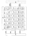
【選択図】図2
Description
Vgs_10C=Vref−Vref_r>Vth_10C・・・・・・1
Vgs_11C=Vref−Vref_r>Vth_11C・・・・・・2
VEE+Vth_10E>Vref_r・・・・・・3
VEE+Vth_11E>Vref_r ・・・・・・4
Vs_10C=Vref−Vth_10C・・・・・・5
Vs_11C=Vref−Vth_11C・・・・・・6
となる。従って、保持容量10B、11Bには、Vth_10C、Vth_11Cがそれぞれ保持される。
VEE+Vth_10E>Vs_10C・・・・・・7
VEE+Vth_11E>Vs_11C・・・・・・8
を満足する必要がある。
VEE+Vth_10E+Vth_10C>Vref・・・・・・9
Vs_10C=Vref−Vth_10C+(Vsig0−Vref)xCap_10E/(Cap_10B+Cap_10E)+VEExCap_10B/(Cap_10B+Cap_10E)
={Cap_10Bx(VEE+Vref)+Cap_10ExVsig0}/(Cap_10B+Cap_10E)−Vth_10C
となり、ゲ−ト電極−ソ−ス電極間の電圧は、
Vgs_10C=Cap_10B/(Cap_10B+Cap_10E)(Vsig0−VEE−Vref)+Vth_10C
となる。
Vs_11C=Vref−Vth_11C+(Vsig0−Vref)xCap_11E/(Cap_11B+Cap_11E)+VEExCap_11B/(Cap_11B+Cap_11E)
となり、ゲ−ト電極−ソ−ス電極間の電圧は、
Vgs_11C=Cap_11B/(Cap_11B+Cap_11E)x(Vsig0−VEE−Vref)+Vth_11C
となる。
Ids0=β/2{Cap_10B/(Cap_10B+Cap_10E)x(Vsig0−VEE−Vref)}2
Ids1=β/2{Cap_11B/(Cap_11B+Cap_11E)x(Vsig1−VEE−Vref)}2
となり、Vthの項は補正され、駆動電流のばらつきを抑えることができる。
Claims (8)
- 一端が信号線に接続され、第1走査線によってオンオフされるサンプリングトランジスタと、
このサンプリングトランジスタの他端にゲートが接続され、ドレインが第1電源に接続される駆動トランジスタと、
この駆動トランジスタのソースと第2電源との間に接続され、前記駆動トランジスタに流れる電流によって駆動される発光素子と、
前記駆動トランジスタのゲート・ソース間に接続される保持容量と、
前記駆動トランジスタのソースと基準電位線の間に配置され、第2走査線によってオンオフされるスイッチングトランジスタと、
を含み、
前記信号線に基準信号電圧が設定されている期間に、前記サンプリングトランジスタと前記スイッチングトランジスタを導通させ、前記駆動トランジスタのゲート・ソース間電圧を前記駆動トランジスタの閾値電圧以上とした状態で前記保持容量に基準信号電圧と基準電位の差電圧を充電すると共に、前記駆動トランジスタのソースの電圧を基準電位に設定することで前記発光素子への印加電圧をその閾値電圧以下とし、
その後、前記信号線に基準信号電圧が設定されている期間に、前記サンプリングトランジスタと前記スイッチングトランジスタを導通させるとともに、前記スイッチングトランジスタをオフにすることで、前記発光素子への印加電圧をその閾値電圧以下に維持したまま、前記保持容量に前記駆動トランジスタの閾値電圧に相当する電圧を保持し、
前記信号線に表示信号電圧が設定されている期間に、前記サンプリングトランジスタを導通させ前記信号電圧をサンプリングし、前記保持容量の保持していた閾値電圧に前記信号電圧を重畳する、
画素回路。 - 複数の画素をマトリクス状に配置した表示装置であって、
複数の信号線と、
この複数の信号線を駆動する信号線駆動回路と、
複数の第1走査線と、
この第1走査線を駆動する第1走査線駆動回路と、
複数の第2走査線と、
この第2走査線を駆動する第2走査線駆動回路と、
基準電位が供給される基準電位線と、
を含み、
各画素は、
一端が信号線に接続され、第1走査線によってオンオフされるサンプリングトランジスタと、
このサンプリングトランジスタの他端にゲートが接続され、ドレインが第1電源に接続される駆動トランジスタと、
この駆動トランジスタのソースと第2電源との間に接続され、前記駆動トランジスタに流れる電流によって駆動される発光素子と、
前記駆動トランジスタのゲート・ソース間に接続される保持容量と、
前記駆動トランジスタのソースと基準電位線の間に配置され、第2走査線によってオンオフされるスイッチングトランジスタと、
を含み、
前記信号線に基準信号電圧が設定されている期間に、前記サンプリングトランジスタと前記スイッチングトランジスタを導通させ、前記駆動トランジスタのゲート・ソース間電圧を前記駆動トランジスタの閾値電圧以上とした状態で前記保持容量に基準信号電圧と基準電位の差電圧を充電すると共に、前記駆動トランジスタのソースの電圧を基準電位に設定することで前記発光素子への印加電圧をその閾値電圧以下とし、
その後、前記信号線に基準信号電圧が設定されている期間に、前記サンプリングトランジスタと前記スイッチングトランジスタを導通させるとともに、前記スイッチングトランジスタをオフにすることで、前記発光素子への印加電圧をその閾値電圧以下に維持したまま、前記保持容量に前記駆動トランジスタの閾値電圧に相当する電圧を保持し、
前記信号線に表示信号電圧が設定されている期間に、前記サンプリングトランジスタを導通させ前記信号電圧をサンプリングし、前記保持容量の保持していた閾値電圧に前記信号電圧を重畳する、
表示装置。 - 請求項2に記載の表示装置であって、
前記基準電位線は、2行の画素に共通であって画素の2行毎に行方向に配置されている表示装置。 - 請求項2に記載の表示装置であって、
前記基準電位線は、2列の画素に共通であって画素の2列毎に列方向に配置されている表示装置。 - 請求項2〜4のいずれか1つに記載の表示装置であって、
前記画素が配列される表示領域の外部において、前記基準電位線をまとめて接続している表示装置。 - 請求項5に記載の表示装置であって、
前記基準電位線に接続されるプローブポイントであって、少なくとも前記発光素子の形成前に、プローブにより外部からポイント可能プローブポイントを有する表示装置。 - 請求項2〜6に記載の表示装置であって、
前記第2走査線は、2行の画素に共通であって画素の2行毎に行方向に配置されている表示装置。 - 請求項2〜7に記載の表示装置についての検査方法であって、
前記発光素子の形成前において、基準電位線にプローブを接続し、各画素における前記サンプリングトランジスタ、スイッチングトランジスタのオンオフを制御して、基準電位線から流れ出る電流を検出することで、駆動トランジスタの電流−電圧特性を測定する表示装置の検査方法。
Priority Applications (8)
| Application Number | Priority Date | Filing Date | Title |
|---|---|---|---|
| JP2009257527A JP5503255B2 (ja) | 2009-11-10 | 2009-11-10 | 画素回路、表示装置および検査方法 |
| KR1020127013445A KR20120105453A (ko) | 2009-11-10 | 2010-11-04 | 픽셀회로, 디스플레이 디바이스 및 검사방법 |
| US13/508,713 US8754882B2 (en) | 2009-11-10 | 2010-11-04 | Pixel circuit, display device, and inspection method |
| EP10830537A EP2499632A4 (en) | 2009-11-10 | 2010-11-04 | PIXEL CIRCUIT, DISPLAY DEVICE, AND INSPECTION METHOD |
| PCT/US2010/055368 WO2011059867A1 (en) | 2009-11-10 | 2010-11-04 | Pixel circuit, display device, and inspection method |
| CN2010800507459A CN102598097A (zh) | 2009-11-10 | 2010-11-04 | 像素电路、显示装置和检查方法 |
| TW099138105A TW201128610A (en) | 2009-11-10 | 2010-11-05 | Pixel circuit, display device, and inspection method |
| US14/276,392 US9569991B2 (en) | 2009-11-10 | 2014-05-13 | Pixel circuit, display device, and inspection method |
Applications Claiming Priority (1)
| Application Number | Priority Date | Filing Date | Title |
|---|---|---|---|
| JP2009257527A JP5503255B2 (ja) | 2009-11-10 | 2009-11-10 | 画素回路、表示装置および検査方法 |
Publications (2)
| Publication Number | Publication Date |
|---|---|
| JP2011102879A true JP2011102879A (ja) | 2011-05-26 |
| JP5503255B2 JP5503255B2 (ja) | 2014-05-28 |
Family
ID=43991963
Family Applications (1)
| Application Number | Title | Priority Date | Filing Date |
|---|---|---|---|
| JP2009257527A Active JP5503255B2 (ja) | 2009-11-10 | 2009-11-10 | 画素回路、表示装置および検査方法 |
Country Status (7)
| Country | Link |
|---|---|
| US (2) | US8754882B2 (ja) |
| EP (1) | EP2499632A4 (ja) |
| JP (1) | JP5503255B2 (ja) |
| KR (1) | KR20120105453A (ja) |
| CN (1) | CN102598097A (ja) |
| TW (1) | TW201128610A (ja) |
| WO (1) | WO2011059867A1 (ja) |
Cited By (2)
| Publication number | Priority date | Publication date | Assignee | Title |
|---|---|---|---|---|
| KR20140117742A (ko) * | 2013-03-26 | 2014-10-08 | 엘지디스플레이 주식회사 | 유기발광 표시장치 및 그 보상장치 |
| KR20150064787A (ko) * | 2013-12-03 | 2015-06-12 | 엘지디스플레이 주식회사 | 유기발광 표시장치 및 그 열화 보상 방법 |
Families Citing this family (15)
| Publication number | Priority date | Publication date | Assignee | Title |
|---|---|---|---|---|
| CN104112432B (zh) * | 2013-04-17 | 2016-10-26 | 瀚宇彩晶股份有限公司 | 显示器 |
| JP6164059B2 (ja) * | 2013-11-15 | 2017-07-19 | ソニー株式会社 | 表示装置、電子機器、及び表示装置の駆動方法 |
| US9443469B2 (en) | 2013-11-22 | 2016-09-13 | Global Oled Technology Llc | Pixel circuit, driving method, display device, and inspection method |
| KR102196908B1 (ko) * | 2014-07-18 | 2020-12-31 | 삼성디스플레이 주식회사 | 유기전계발광 표시장치 및 그의 구동방법 |
| KR102177216B1 (ko) * | 2014-10-10 | 2020-11-11 | 삼성디스플레이 주식회사 | 표시 장치 및 표시 장치 제어 방법 |
| KR102230928B1 (ko) * | 2014-10-13 | 2021-03-24 | 삼성디스플레이 주식회사 | 유기 발광 표시 장치 및 이의 구동 방법 |
| CN104464586B (zh) * | 2014-12-30 | 2017-02-22 | 京东方科技集团股份有限公司 | 显示面板检测装置及显示面板的检测方法 |
| CN104658482B (zh) * | 2015-03-16 | 2017-05-31 | 深圳市华星光电技术有限公司 | Amoled像素驱动电路及像素驱动方法 |
| JP6804255B2 (ja) * | 2015-12-15 | 2020-12-23 | 三星エスディアイ株式会社Samsung SDI Co., Ltd. | 電極形成用組成物ならびにこれを用いて製造された電極および太陽電池 |
| KR102526484B1 (ko) * | 2015-12-30 | 2023-04-26 | 엘지디스플레이 주식회사 | 유기발광다이오드표시장치 및 이의 구동방법 |
| KR102366285B1 (ko) * | 2015-12-31 | 2022-02-23 | 엘지디스플레이 주식회사 | 유기발광 표시장치 및 이의 구동방법 |
| CN108091301B (zh) * | 2017-12-14 | 2020-06-09 | 京东方科技集团股份有限公司 | 电压采样电路、方法及显示装置 |
| KR102732236B1 (ko) * | 2019-04-17 | 2024-11-21 | 삼성디스플레이 주식회사 | 복수의 데이터 드라이버들을 포함하는 표시 장치 |
| CN111044874B (zh) * | 2019-12-31 | 2022-05-24 | 武汉天马微电子有限公司 | 一种显示模组、检测方法及电子设备 |
| KR102164276B1 (ko) * | 2020-02-27 | 2020-10-12 | 엘지디스플레이 주식회사 | 유기전계발광 표시장치와, 그 표시패널 및 구동방법 |
Citations (7)
| Publication number | Priority date | Publication date | Assignee | Title |
|---|---|---|---|---|
| JP2004191603A (ja) * | 2002-12-10 | 2004-07-08 | Semiconductor Energy Lab Co Ltd | 表示装置およびその検査方法 |
| JP2004334204A (ja) * | 2003-04-30 | 2004-11-25 | Eastman Kodak Co | 4色有機発光デバイス |
| JP2005285631A (ja) * | 2004-03-30 | 2005-10-13 | Casio Comput Co Ltd | 画素回路基板、画素回路基板の検査方法、トランジスタ群、トランジスタ群の検査方法、検査装置 |
| JP2006139079A (ja) * | 2004-11-12 | 2006-06-01 | Eastman Kodak Co | 発光パネル用基板、発光パネル用基板の検査方法及び発光パネル |
| JP2008052111A (ja) * | 2006-08-25 | 2008-03-06 | Mitsubishi Electric Corp | Tftアレイ基板、その検査方法および表示装置 |
| JP2009157019A (ja) * | 2007-12-26 | 2009-07-16 | Sony Corp | 表示装置と電子機器 |
| WO2009087746A1 (ja) * | 2008-01-07 | 2009-07-16 | Panasonic Corporation | 表示装置、電子装置及び駆動方法 |
Family Cites Families (19)
| Publication number | Priority date | Publication date | Assignee | Title |
|---|---|---|---|---|
| DE3235119A1 (de) * | 1982-09-22 | 1984-03-22 | Siemens AG, 1000 Berlin und 8000 München | Anordnung fuer die pruefung von mikroverdrahtungen und verfahren zu ihrem betrieb |
| JP3800404B2 (ja) * | 2001-12-19 | 2006-07-26 | 株式会社日立製作所 | 画像表示装置 |
| JP3613253B2 (ja) | 2002-03-14 | 2005-01-26 | 日本電気株式会社 | 電流制御素子の駆動回路及び画像表示装置 |
| GB0218170D0 (en) | 2002-08-06 | 2002-09-11 | Koninkl Philips Electronics Nv | Electroluminescent display devices |
| JP4409821B2 (ja) * | 2002-11-21 | 2010-02-03 | 奇美電子股▲ふん▼有限公司 | El表示装置 |
| US7265572B2 (en) | 2002-12-06 | 2007-09-04 | Semicondcutor Energy Laboratory Co., Ltd. | Image display device and method of testing the same |
| GB0307475D0 (en) | 2003-04-01 | 2003-05-07 | Koninkl Philips Electronics Nv | Active matrix display devices |
| US7173590B2 (en) | 2004-06-02 | 2007-02-06 | Sony Corporation | Pixel circuit, active matrix apparatus and display apparatus |
| CA2472671A1 (en) * | 2004-06-29 | 2005-12-29 | Ignis Innovation Inc. | Voltage-programming scheme for current-driven amoled displays |
| US7071717B2 (en) * | 2004-10-28 | 2006-07-04 | Agilent Technologies, Inc. | Universal test fixture |
| US7317434B2 (en) | 2004-12-03 | 2008-01-08 | Dupont Displays, Inc. | Circuits including switches for electronic devices and methods of using the electronic devices |
| CN101313349B (zh) * | 2005-11-29 | 2010-12-01 | 京瓷株式会社 | 图像显示装置 |
| FR2900492B1 (fr) * | 2006-04-28 | 2008-10-31 | Thales Sa | Ecran electroluminescent organique |
| KR101245218B1 (ko) * | 2006-06-22 | 2013-03-19 | 엘지디스플레이 주식회사 | 유기발광다이오드 표시소자 |
| KR101031694B1 (ko) | 2007-03-29 | 2011-04-29 | 도시바 모바일 디스플레이 가부시키가이샤 | El 표시 장치 |
| KR101361981B1 (ko) * | 2008-02-19 | 2014-02-21 | 엘지디스플레이 주식회사 | 유기발광다이오드 표시장치와 그 구동방법 |
| JP4737221B2 (ja) * | 2008-04-16 | 2011-07-27 | ソニー株式会社 | 表示装置 |
| US7863123B2 (en) * | 2009-01-19 | 2011-01-04 | International Business Machines Corporation | Direct contact between high-κ/metal gate and wiring process flow |
| TWI417840B (zh) * | 2009-08-26 | 2013-12-01 | Au Optronics Corp | 畫素電路、主動式矩陣有機發光二極體顯示器及畫素電路之驅動方法 |
-
2009
- 2009-11-10 JP JP2009257527A patent/JP5503255B2/ja active Active
-
2010
- 2010-11-04 EP EP10830537A patent/EP2499632A4/en not_active Withdrawn
- 2010-11-04 US US13/508,713 patent/US8754882B2/en active Active
- 2010-11-04 CN CN2010800507459A patent/CN102598097A/zh active Pending
- 2010-11-04 KR KR1020127013445A patent/KR20120105453A/ko not_active Withdrawn
- 2010-11-04 WO PCT/US2010/055368 patent/WO2011059867A1/en not_active Ceased
- 2010-11-05 TW TW099138105A patent/TW201128610A/zh unknown
-
2014
- 2014-05-13 US US14/276,392 patent/US9569991B2/en active Active
Patent Citations (7)
| Publication number | Priority date | Publication date | Assignee | Title |
|---|---|---|---|---|
| JP2004191603A (ja) * | 2002-12-10 | 2004-07-08 | Semiconductor Energy Lab Co Ltd | 表示装置およびその検査方法 |
| JP2004334204A (ja) * | 2003-04-30 | 2004-11-25 | Eastman Kodak Co | 4色有機発光デバイス |
| JP2005285631A (ja) * | 2004-03-30 | 2005-10-13 | Casio Comput Co Ltd | 画素回路基板、画素回路基板の検査方法、トランジスタ群、トランジスタ群の検査方法、検査装置 |
| JP2006139079A (ja) * | 2004-11-12 | 2006-06-01 | Eastman Kodak Co | 発光パネル用基板、発光パネル用基板の検査方法及び発光パネル |
| JP2008052111A (ja) * | 2006-08-25 | 2008-03-06 | Mitsubishi Electric Corp | Tftアレイ基板、その検査方法および表示装置 |
| JP2009157019A (ja) * | 2007-12-26 | 2009-07-16 | Sony Corp | 表示装置と電子機器 |
| WO2009087746A1 (ja) * | 2008-01-07 | 2009-07-16 | Panasonic Corporation | 表示装置、電子装置及び駆動方法 |
Cited By (4)
| Publication number | Priority date | Publication date | Assignee | Title |
|---|---|---|---|---|
| KR20140117742A (ko) * | 2013-03-26 | 2014-10-08 | 엘지디스플레이 주식회사 | 유기발광 표시장치 및 그 보상장치 |
| KR102017673B1 (ko) * | 2013-03-26 | 2019-09-04 | 엘지디스플레이 주식회사 | 유기발광 표시장치 및 그 보상장치 |
| KR20150064787A (ko) * | 2013-12-03 | 2015-06-12 | 엘지디스플레이 주식회사 | 유기발광 표시장치 및 그 열화 보상 방법 |
| KR102067228B1 (ko) * | 2013-12-03 | 2020-01-17 | 엘지디스플레이 주식회사 | 유기발광 표시장치 및 그 열화 보상 방법 |
Also Published As
| Publication number | Publication date |
|---|---|
| TW201128610A (en) | 2011-08-16 |
| US8754882B2 (en) | 2014-06-17 |
| WO2011059867A8 (en) | 2013-06-06 |
| EP2499632A1 (en) | 2012-09-19 |
| EP2499632A4 (en) | 2013-04-03 |
| KR20120105453A (ko) | 2012-09-25 |
| US20130016083A1 (en) | 2013-01-17 |
| WO2011059867A1 (en) | 2011-05-19 |
| JP5503255B2 (ja) | 2014-05-28 |
| CN102598097A (zh) | 2012-07-18 |
| US20140239961A1 (en) | 2014-08-28 |
| US9569991B2 (en) | 2017-02-14 |
Similar Documents
| Publication | Publication Date | Title |
|---|---|---|
| JP5503255B2 (ja) | 画素回路、表示装置および検査方法 | |
| US11217154B2 (en) | Pixel circuit and display panel | |
| JP4203773B2 (ja) | 表示装置 | |
| JP4203772B2 (ja) | 表示装置およびその駆動方法 | |
| US7106089B2 (en) | Inspection device and inspection method for active matrix panel, and manufacturing method for active matrix organic light emitting diode panel | |
| JP5308796B2 (ja) | 表示装置および画素回路 | |
| US9640109B2 (en) | Pixel driving circuit, pixel driving method, display panel and display device | |
| US10783827B2 (en) | Display device and driving method thereof | |
| CN100495507C (zh) | 发光显示器 | |
| CN101996582B (zh) | 有机发光二极管的像素驱动电路 | |
| JP2008032863A (ja) | 表示装置およびその駆動方法 | |
| CN101430862A (zh) | 有机电致发光显示器件的驱动装置 | |
| JP2007310311A (ja) | 表示装置及びその駆動方法 | |
| CN101996579A (zh) | 有源有机电致发光显示器的像素驱动电路及其驱动方法 | |
| US20070195019A1 (en) | Image display apparatus | |
| KR20140135618A (ko) | 전기 광학 장치 및 그 구동 방법 | |
| JP2008122632A (ja) | 表示装置 | |
| JP2008032863A5 (ja) | ||
| CN101697268A (zh) | 有机发光二极管显示器、像素电路及数据电流写入方法 | |
| CN101221723B (zh) | 电致发光显示装置和电致发光显示装置的显示偏差补偿方法 | |
| JP2008139520A (ja) | 表示装置 | |
| CN209785530U (zh) | 一种像素补偿电路 | |
| JP2008310075A (ja) | 画像表示装置 | |
| KR20160083613A (ko) | 유기발광 표시장치와 이의 구동방법 | |
| KR20150141451A (ko) | 유기발광다이오드 표시장치 및 그 제조방법 |
Legal Events
| Date | Code | Title | Description |
|---|---|---|---|
| A621 | Written request for application examination |
Free format text: JAPANESE INTERMEDIATE CODE: A621 Effective date: 20120611 |
|
| A977 | Report on retrieval |
Free format text: JAPANESE INTERMEDIATE CODE: A971007 Effective date: 20130115 |
|
| A131 | Notification of reasons for refusal |
Free format text: JAPANESE INTERMEDIATE CODE: A131 Effective date: 20130219 |
|
| A521 | Request for written amendment filed |
Free format text: JAPANESE INTERMEDIATE CODE: A523 Effective date: 20130507 |
|
| A521 | Request for written amendment filed |
Free format text: JAPANESE INTERMEDIATE CODE: A523 Effective date: 20130520 |
|
| A131 | Notification of reasons for refusal |
Free format text: JAPANESE INTERMEDIATE CODE: A131 Effective date: 20130806 |
|
| A521 | Request for written amendment filed |
Free format text: JAPANESE INTERMEDIATE CODE: A523 Effective date: 20131001 |
|
| A131 | Notification of reasons for refusal |
Free format text: JAPANESE INTERMEDIATE CODE: A131 Effective date: 20131210 |
|
| A521 | Request for written amendment filed |
Free format text: JAPANESE INTERMEDIATE CODE: A523 Effective date: 20131219 |
|
| TRDD | Decision of grant or rejection written | ||
| A01 | Written decision to grant a patent or to grant a registration (utility model) |
Free format text: JAPANESE INTERMEDIATE CODE: A01 Effective date: 20140311 |
|
| A61 | First payment of annual fees (during grant procedure) |
Free format text: JAPANESE INTERMEDIATE CODE: A61 Effective date: 20140314 |
|
| R150 | Certificate of patent or registration of utility model |
Ref document number: 5503255 Country of ref document: JP Free format text: JAPANESE INTERMEDIATE CODE: R150 |
|
| R250 | Receipt of annual fees |
Free format text: JAPANESE INTERMEDIATE CODE: R250 |
|
| R250 | Receipt of annual fees |
Free format text: JAPANESE INTERMEDIATE CODE: R250 |
|
| R250 | Receipt of annual fees |
Free format text: JAPANESE INTERMEDIATE CODE: R250 |
|
| R250 | Receipt of annual fees |
Free format text: JAPANESE INTERMEDIATE CODE: R250 |
|
| R250 | Receipt of annual fees |
Free format text: JAPANESE INTERMEDIATE CODE: R250 |
|
| R250 | Receipt of annual fees |
Free format text: JAPANESE INTERMEDIATE CODE: R250 |
|
| R250 | Receipt of annual fees |
Free format text: JAPANESE INTERMEDIATE CODE: R250 |
|
| R250 | Receipt of annual fees |
Free format text: JAPANESE INTERMEDIATE CODE: R250 |
|
| R250 | Receipt of annual fees |
Free format text: JAPANESE INTERMEDIATE CODE: R250 |
|
| R250 | Receipt of annual fees |
Free format text: JAPANESE INTERMEDIATE CODE: R250 |