JP2011106987A - Electricity source and method for determining useful life of capacitor - Google Patents
Electricity source and method for determining useful life of capacitor Download PDFInfo
- Publication number
- JP2011106987A JP2011106987A JP2009262922A JP2009262922A JP2011106987A JP 2011106987 A JP2011106987 A JP 2011106987A JP 2009262922 A JP2009262922 A JP 2009262922A JP 2009262922 A JP2009262922 A JP 2009262922A JP 2011106987 A JP2011106987 A JP 2011106987A
- Authority
- JP
- Japan
- Prior art keywords
- smoothing capacitor
- power supply
- charging
- life
- voltage
- Prior art date
- Legal status (The legal status is an assumption and is not a legal conclusion. Google has not performed a legal analysis and makes no representation as to the accuracy of the status listed.)
- Withdrawn
Links
Images

Classifications
-
- Y—GENERAL TAGGING OF NEW TECHNOLOGICAL DEVELOPMENTS; GENERAL TAGGING OF CROSS-SECTIONAL TECHNOLOGIES SPANNING OVER SEVERAL SECTIONS OF THE IPC; TECHNICAL SUBJECTS COVERED BY FORMER USPC CROSS-REFERENCE ART COLLECTIONS [XRACs] AND DIGESTS
- Y02—TECHNOLOGIES OR APPLICATIONS FOR MITIGATION OR ADAPTATION AGAINST CLIMATE CHANGE
- Y02B—CLIMATE CHANGE MITIGATION TECHNOLOGIES RELATED TO BUILDINGS, e.g. HOUSING, HOUSE APPLIANCES OR RELATED END-USER APPLICATIONS
- Y02B20/00—Energy efficient lighting technologies, e.g. halogen lamps or gas discharge lamps
- Y02B20/40—Control techniques providing energy savings, e.g. smart controller or presence detection
Landscapes
- Testing Electric Properties And Detecting Electric Faults (AREA)
- Circuit Arrangement For Electric Light Sources In General (AREA)
- Rectifiers (AREA)
- Power Conversion In General (AREA)
Abstract
【課題】直流を平滑するコンデンサの寿命を正確に判定することができる電源装置及びコンデンサ寿命判定方法を提供する。
【解決手段】電源電圧の0V電圧のタイミングで平滑コンデンサ3に充電を行い、充電開始直後の平滑コンデンサ3の充電電流のピーク値ΔVと、該ピーク値ΔVに到達するまでのピーク電流到達時間Δtを求める。そして、求めたピーク値ΔVを寿命の判定基準値Vrefと比較し、さらにピーク電流到達時間Δtを判定基準時間Trefと比較する。この比較において、ピーク値ΔVが寿命の判定基準値Vref以下で、かつピーク電流到達時間Δtが判定基準時間Tref以下であれば、平滑コンデンサ3が寿命であると判定する。
【選択図】図1A power supply device and a capacitor life determination method capable of accurately determining the life of a capacitor that smoothes a direct current are provided.
The smoothing capacitor is charged at the timing of 0 V voltage of the power supply voltage, the peak value ΔV of the charging current of the smoothing capacitor immediately after the start of charging, and the peak current arrival time Δt until the peak value ΔV is reached. Ask for. Then, the obtained peak value ΔV is compared with the lifetime determination reference value Vref, and the peak current arrival time Δt is compared with the determination reference time Tref. In this comparison, if the peak value ΔV is equal to or less than the lifetime determination reference value Vref and the peak current arrival time Δt is equal to or less than the determination reference time Tref, it is determined that the smoothing capacitor 3 is at the lifetime.
[Selection] Figure 1
Description
本発明は、直流電源をコンデンサで平滑して直流電圧を出力する電源装置及びコンデンサ寿命判定方法に関する。 The present invention relates to a power supply apparatus that outputs a DC voltage by smoothing a DC power supply with a capacitor and a capacitor life determination method.
従来、特許文献1や特許文献2にも記載されているように、直流電源を平滑するコンデンサ(主に電解コンデンサ)の電気的な特性を検出して寿命を判断する方法が案出されている。すなわち、特許文献1には、点灯装置内のコンデンサの容量が寿命末期に低下することにより、充放電の時間が初期に比べて短くなることを検出して寿命を判定する技術が開示されている。特許文献2には、コンデンサの放電時間を計測するカウンタを備えて、計測した放電時間が基準となる放電時間よりも短くなったときに、コンデンサが交換時期である旨を表示器で表示する技術が開示されている。
Conventionally, as described in
しかしながら、特許文献1に記載されている電源投入時にコンデンサの電圧を検出する方法では、電源投入の位相角により波形が異なることを考慮していないため 、コンデンサの端子電圧を正確に検出することができない。また、この文献には、力率改善回路(PFC(Power Factor Control)回路)に対応する検出回路が開示されていない。特許文献2に記載されている電源遮断時にコンデンサの端子電圧を検出する方法では、電源遮断時においてコンデンサの特性を検知するので、コンデンサの動作中における容量抜け等の異常を検知することができない。このように、特許文献1及び2に記載された技術では、コンデンサの寿命を正確に判定することは困難である。
However, the method for detecting the voltage of the capacitor at the time of power-on described in
本発明は、係る事情に鑑みてなされたものであり、直流を平滑するコンデンサの寿命を正確に判定することができる電源装置及びコンデンサ寿命判定方法を提供することを目的とする。 The present invention has been made in view of such circumstances, and an object of the present invention is to provide a power supply device and a capacitor life determination method that can accurately determine the life of a capacitor that smoothes a direct current.
本発明の電源装置は、交流電源を整流する整流器と、前記整流器から出力される直流電源を平滑して直流電圧を出力する平滑コンデンサと、前記交流電源の周波数及びピーク電圧値を計測する電源計測手段と、前記電源計測手段による計測に基づき、0V電圧のタイミングで前記平滑コンデンサに充電を行う充電制御手段と、前記平滑コンデンサの充電時における充電電流を検出する充電電流検出手段と、前記充電電流検出手段で検出された充電開始直後の前記平滑コンデンサへの突入電流特性から前記平滑コンデンサの寿命を判定する平滑コンデンサ寿命判定手段と、を備えた。 The power supply apparatus of the present invention includes a rectifier that rectifies an AC power supply, a smoothing capacitor that outputs a DC voltage by smoothing a DC power output from the rectifier, and a power supply measurement that measures a frequency and a peak voltage value of the AC power supply. Means, charging control means for charging the smoothing capacitor at a timing of 0 V voltage based on measurement by the power supply measuring means, charging current detection means for detecting a charging current when charging the smoothing capacitor, and the charging current Smoothing capacitor life judging means for judging the life of the smoothing capacitor from the inrush current characteristic to the smoothing capacitor immediately after the start of charging detected by the detecting means.
上記構成によれば、電源電圧の0V電圧のタイミングで平滑コンデンサに充電を行い、充電開始直後の平滑コンデンサへの突入電流特性から平滑コンデンサの寿命を判定するので、電源位相や電圧変化による誤差を低減でき、正確に平滑コンデンサの寿命を判定することができる。また、電源電圧0V位相から充電を開始するので、突入電流の抑制ができるので、突入電流を抑制するための専用の回路が不要となり、コストの低減が可能となる。 According to the above configuration, the smoothing capacitor is charged at the timing of 0 V of the power supply voltage, and the life of the smoothing capacitor is determined from the inrush current characteristics to the smoothing capacitor immediately after the start of charging. The life of the smoothing capacitor can be accurately determined. In addition, since charging is started from the phase of the power supply voltage 0V, the inrush current can be suppressed, so that a dedicated circuit for suppressing the inrush current is not necessary, and the cost can be reduced.
上記構成において、前記整流器の出力端と前記平滑コンデンサの間に直列に介挿される第1のスイッチと抵抗からなる直列回路と、前記直列回路と並列に介挿される第2のスイッチと、を備え、前記充電制御手段は、0V電圧のタイミングで前記直列回路の前記第1のスイッチをオン状態にして前記平滑コンデンサに充電を行い、前記平滑コンデンサへの充電が完了すると前記第2のスイッチをオンする。 In the above configuration, a first circuit inserted in series between the output terminal of the rectifier and the smoothing capacitor and a resistor, and a second switch inserted in parallel with the series circuit are provided. The charging control means turns on the first switch of the series circuit at a timing of 0 V voltage to charge the smoothing capacitor, and turns on the second switch when the charging to the smoothing capacitor is completed. To do.
上記構成によれば、平滑コンデンサの寿命判定後に、平滑コンデンサの充電電流を検出するための抵抗を回路から外すことができ、この抵抗による電力消費を削減できる。 According to the above configuration, after determining the life of the smoothing capacitor, the resistor for detecting the charging current of the smoothing capacitor can be removed from the circuit, and power consumption due to this resistor can be reduced.
上記構成において、前記平滑コンデンサ寿命判定手段は、前記平滑コンデンサの充電電流のピーク値から前記平滑コンデンサの寿命を判定する。 The said structure WHEREIN: The said smoothing capacitor lifetime determination means determines the lifetime of the said smoothing capacitor from the peak value of the charging current of the said smoothing capacitor.
上記構成によれば、平滑コンデンサの充電電流のピーク値の違いで平滑コンデンサの寿命を判定することができる。平滑コンデンサの静電容量が小さいときは充電電流のピーク値が小さくなり、静電容量が大きいときは充電電流のピーク値は大きくなる。コンデンサは寿命近くなると静電容量が小さくなることから、充電電流のピーク値の違いをみることで平滑コンデンサの寿命を容易に判定することができる。 According to the said structure, the lifetime of a smoothing capacitor can be determined by the difference in the peak value of the charging current of a smoothing capacitor. When the capacitance of the smoothing capacitor is small, the peak value of the charging current is small, and when the capacitance is large, the peak value of the charging current is large. Since the capacitance of the capacitor becomes smaller when it is near the end of its life, the life of the smoothing capacitor can be easily determined by looking at the difference in the peak value of the charging current.
上記構成において、前記平滑コンデンサ寿命判定手段は、前記平滑コンデンサの充電電流のピーク値到達時間変化から前記平滑コンデンサの寿命を判定する。 In the above-described configuration, the smoothing capacitor life determination means determines the life of the smoothing capacitor from a change in the peak value arrival time of the charging current of the smoothing capacitor.
上記構成によれば、平滑コンデンサの充電電流のピーク値到達時間変化から平滑コンデンサの寿命を判定することができる。平滑コンデンサの静電容量が小さいときは充電電流のピーク値に到達するまでの時間が早くなり、静電容量が大きいときは充電電流のピーク値に到達するまでの時間が遅くなる。コンデンサは寿命近くなると静電容量が小さくなることから、充電電流のピーク値に到達するまでの時間の違いをみることで平滑コンデンサの寿命を容易に判定することができる。 According to the above configuration, the life of the smoothing capacitor can be determined from the change in the peak value arrival time of the charging current of the smoothing capacitor. When the capacitance of the smoothing capacitor is small, the time until the peak value of the charging current is reached is shortened, and when the capacitance is large, the time until the peak value of the charging current is reached is delayed. Since the capacitance of the capacitor decreases as it approaches the end of its life, the life of the smoothing capacitor can be easily determined by looking at the difference in time until the peak value of the charging current is reached.
上記構成において、前記平滑コンデンサ寿命判定手段は、前記平滑コンデンサの充電電流のピーク値と該ピーク値までの到達時間から前記平滑コンデンサの寿命を判定する。 In the above configuration, the smoothing capacitor life determination means determines the life of the smoothing capacitor from the peak value of the charging current of the smoothing capacitor and the arrival time to the peak value.
上記構成によれば、平滑コンデンサの充電電流のピーク値の違いと、ピーク値到達時間変化の両面からみることで、それぞれを単独でみる場合よりもさらに正確に平滑コンデンサの寿命を判定することができる。 According to the above configuration, the lifetime of the smoothing capacitor can be determined more accurately than in the case where each is viewed alone, by looking at both the difference in the peak value of the charging current of the smoothing capacitor and the change in the peak value arrival time. it can.
本発明の照明装置は、上記電源装置を備えた。 The illuminating device of this invention was equipped with the said power supply device.
上記構成によれば、平滑コンデンサの寿命を正確に判定することができる照明装置を提供でき、常に効率の良い照明が可能となる。 According to the said structure, the illuminating device which can determine the lifetime of a smoothing capacitor correctly can be provided, and always efficient illumination is attained.
本発明のコンデンサ寿命判定方法は、交流電源を整流する整流器から出力される直流電源を平滑して直流電圧を出力する平滑コンデンサ備える電源装置における前記平滑コンデンサの寿命を判定するコンデンサ寿命判定方法であって、前記交流電源の周波数及びピーク電圧値を計測する電源計測ステップと、前記電源計測ステップによる計測に基づき、0V電圧のタイミングで前記平滑コンデンサに充電を行う充電ステップと、前記平滑コンデンサの充電時における充電電流を検出する充電電流検出ステップと、前記充電電流検出ステップで検出された充電開始直後の前記平滑コンデンサへの突入電流特性から前記平滑コンデンサの寿命を判定する平滑コンデンサ寿命判定ステップと、を備えた。 The capacitor life determination method of the present invention is a capacitor life determination method for determining the life of the smoothing capacitor in a power supply device including a smoothing capacitor that outputs a DC voltage by smoothing a DC power output from a rectifier that rectifies an AC power supply. A power source measuring step for measuring the frequency and peak voltage value of the AC power source, a charging step for charging the smoothing capacitor at a timing of 0 V voltage based on the measurement by the power source measuring step, and at the time of charging the smoothing capacitor A charging current detection step for detecting a charging current in step, and a smoothing capacitor life determination step for determining the life of the smoothing capacitor from the inrush current characteristics to the smoothing capacitor immediately after the start of charging detected in the charging current detection step. Prepared.
上記方法によれば、電源電圧の0V電圧のタイミングで平滑コンデンサに充電を行い、充電開始直後の平滑コンデンサへの突入電流特性から平滑コンデンサの寿命を判定するので、電源位相や電圧変化による誤差を低減でき、正確に平滑コンデンサの寿命を判定することができる。また、電源電圧0V位相から充電を開始するので、突入電流の抑制ができるので、突入電流を抑制するための専用の回路が不要となり、コストの低減が可能となる。 According to the above method, the smoothing capacitor is charged at the timing of 0 V of the power supply voltage, and the life of the smoothing capacitor is determined from the inrush current characteristic to the smoothing capacitor immediately after the start of charging. The life of the smoothing capacitor can be accurately determined. In addition, since charging is started from the phase of the power supply voltage 0V, the inrush current can be suppressed, so that a dedicated circuit for suppressing the inrush current is not necessary, and the cost can be reduced.
本発明は、電源装置における平滑コンデンサの寿命を正確に判定することができる。 The present invention can accurately determine the life of a smoothing capacitor in a power supply device.
以下、本発明を実施するための好適な実施の形態について、図面を参照して詳細に説明する。 DESCRIPTION OF EXEMPLARY EMBODIMENTS Hereinafter, preferred embodiments for carrying out the invention will be described in detail with reference to the drawings.
(実施の形態1)
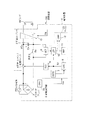
図1は、本発明の実施の形態1に係る電源装置の回路構成図である。同図において、本実施の形態の電源装置1は、ダイオードブリッジ2と、平滑コンデンサ(電解コンデンサ)3と、平滑コンデンサ充電スイッチ4と、抵抗(Rs)5と、平滑コンデンサ電流検出回路(DET)6と、入力電源電圧検出回路(DET2)7と、充電開始信号出力回路(LDC)8と、充電制御回路(CC1)9と、ピーク電流・時間検出回路(ΔV)10と、基準電圧発生回路(REF)11と、比較回路(CMP)12と、制御電源回路(CPS)14と、インバータ回路15と、を備える。
(Embodiment 1)
FIG. 1 is a circuit configuration diagram of a power supply device according to
ダイオードブリッジ2は、交流電源を全波整流して直流電源を出力する。平滑コンデンサ3は、ダイオードブリッジ2から出力される直流電源を平滑する。平滑コンデンサ充電スイッチ4は、例えばサイリスタで構成され、ダイオードブリッジ2と平滑コンデンサ3の間の高圧側に直列に介挿される。平滑コンデンサ充電スイッチ4は、充電制御回路9からのオン信号でオン状態(導通状態)となる。なお、平滑コンデンサ充電スイッチ4をサイリスタで構成する場合、サイリスタのカソードが平滑コンデンサ3側(インバータ回路15側)に接続され、アノードがダイオードブリッジ2側に接続され、ゲートが充電制御回路9に接続されることで平滑コンデンサ充電スイッチ4をオン状態にする。
The
ピーク電流・時間検出回路10は、充電開始信号出力回路8から充電開始信号S1が出力されるタイミングで、平滑コンデンサ電流検出回路6から出力された平滑コンデンサ3の充電電流のピーク値ΔVを検出し、また該ピーク値ΔVに至るまでの時間(ピーク電流到達時間)Δtを求める。
The peak current /
基準電圧発生回路11は、ピーク電流・時間検出回路10で検出された平滑コンデンサ3のピーク値ΔVが供給される比較回路12に接続される。
The reference
抵抗5は、ダイオードブリッジ2と平滑コンデンサ3の間の低圧側に直列に介挿される。平滑コンデンサ電流検出回路6は、抵抗5の両端電圧を検出することで平滑コンデンサ3に流れる電流を検出する。入力電源電圧検出回路7は、ダイオードブリッジ2からの直流電源(脈流)を検出して交流電源PSの周波数及びピーク電圧値を計測し、計測結果を充電開始信号出力回路8へ出力する。充電開始信号出力回路8は、入力電源電圧検出回路7で検出された直流電源から0V電圧のタイミングで充電開始信号S1を充電制御回路9及びピーク電流・時間検出回路10へ出力する。充電制御回路9は、平滑コンデンサ充電スイッチ4をオン/オフ制御するものであり、充電開始信号出力回路8から充電開始信号S1がピーク値ΔVと比較するための寿命の判定基準値Vrefとピーク電流到達時間Δtの判定基準時間Trefを出力する。比較回路12は、ピーク電流・時間検出回路10で検出された平滑コンデンサ3の充電電流のピーク値ΔVと基準電圧発生回路11から出力された寿命の判定基準値Vrefを比較するとともに、ピーク電流到達時間Δtと判定基準時間Trefを比較し、ピーク値ΔVが寿命の判定基準値Vref以下で、かつピーク電流到達時間Δtが判定基準時間Tref以下であれば、平滑コンデンサ3の寿命を検知する。比較回路12は、平滑コンデンサ3の寿命を検知すると、インバータ起動信号ENを出力せず、インバータ回路15を停止状態にする。
The
制御電源回路14は、ダイオードブリッジ2から出力される直流電源で動作し、上記各部6〜12を構成するマイクロコンピュータ(以下、“マイコン”と呼ぶ)13に直流電源Vccを供給する。インバータ回路15は、比較回路12からインバータ起動信号ENが出力されることで起動し、平滑コンデンサ3の平滑作用で得られた直流電圧を交流電圧に変換してランプ16へ出力する。
The control
なお、上記ダイオードブリッジ2は整流器に対応する。また、上記平滑コンデンサ充電スイッチ4は第1のスイッチに対応する。また、上記入力電源電圧検出回路7は入力電源電圧検出手段に対応する。また、上記充電開始信号出力回路8と充電制御回路9は充電制御手段を構成する。また、上記抵抗5、平滑コンデンサ電流検出回路6及びピーク電流・時間検出回路10は充電電流検出手段を構成する。また、上記基準電圧発生回路11と比較回路12は平滑コンデンサ寿命判定手段を構成する。また、電源装置1とランプ16は照明装置100を構成する。
The
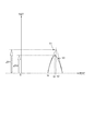
次に、図2及び図3に示す動作波形図を参照しながら上記構成の電源装置1の動作を説明する。図2において、“DET2”は入力電源電圧検出回路7の出力電圧の波形図、“Vcc”は制御電源回路14の出力電圧の波形図、“SW1”は平滑コンデンサ充電スイッチ4のオン/オフ状態を示す波形図、“DET”は平滑コンデンサ電流検出回路6の出力電圧の波形図、“VCx”は平滑コンデンサ3の端子電圧の波形図である。
Next, the operation of the
電源投入によってマイコン13に直流電圧Vccが印加されてマイコン13が動作を開始する。最初の0V電圧のタイミング(t1)の次の0V電圧のタイミング(t2)で充電開始信号出力回路8が充電開始信号S1を出力して平滑コンデンサ充電スイッチ4をオン状態にする。また、充電開始信号S1が出力されることでピーク電流・時間検出回路10が動作を開始し、平滑コンデンサ電流検出回路6にて検出された平滑コンデンサ3の充電電流のピーク値ΔVを検出し、また該ピーク値に至るまでのピーク電流到達時間Δtを求める。この場合、ピーク電流到達時間Δtはt3−t2となる。
When power is turned on, the DC voltage Vcc is applied to the
ここで、ピーク値ΔVは、平滑コンデンサ3の静電容量が小さいときは小さくなり、静電容量が大きいときは大きくなる。図3は図2の平滑コンデンサ電流検出回路6の出力電圧を拡大した図であり、この図におけるV1は正常時の出力電圧波形、V2は寿命時の出力電圧波形である。平滑コンデンサ3の静電容量が小さいときはピーク値に到達するまでの時間が早くなり、静電容量が大きいときはピーク値に到達するまでの時間が遅くなる。これは電源と平滑コンデンサ3の間に存在する抵抗成分によって生じる。
Here, the peak value ΔV decreases when the capacitance of the smoothing
平滑コンデンサ充電スイッチ4がオン状態になると、その時点から平滑コンデンサ3への充電が開始され、平滑コンデンサ3の端子電圧VCxが徐々に上昇して行き、平滑コンデンサ電流検出回路6から平滑コンデンサ3の充電電流の検出値が出力される。そして、ピーク電流・時間検出回路10で平滑コンデンサ3の充電電流のピーク値ΔV及びピーク電流到達時間Δtの検出が行われる。この動作は、次の0V電圧のタイミング(t4)でも同様に行われるが、このときは平滑コンデンサ3の充電電流のピーク値ΔV及びピーク電流到達時間Δtの検出は行われない。
When the smoothing capacitor charging switch 4 is turned on, charging to the smoothing
充電開始から所定時間を経過すると平滑コンデンサ3には充電電流が無くなり、平滑コンデンサ3の充電電流の計測が終了する。
When a predetermined time has elapsed from the start of charging, the smoothing
平滑コンデンサ3の充電電流のピーク値ΔVが検出され、ピーク電流到達時間Δtが求められると、比較回路12がピーク値ΔVを寿命の判定基準値Vrefと比較し、さらにピーク電流到達時間Δtを判定基準時間Trefと比較する。この比較において、ピーク値ΔVが寿命の判定基準値Vref以下で、かつピーク電流到達時間Δtが判定基準時間Tref以下であれば、平滑コンデンサ3が寿命であると判定する。平滑コンデンサ3が寿命であると判定した場合、比較回路12はインバータ起動信号ENを出力せず、インバータ回路15を停止状態にする。
When the peak value ΔV of the charging current of the smoothing
このように本実施の形態の電源装置1は、電源電圧の0V電圧のタイミングで平滑コンデンサ3に充電を行い、充電開始直後の平滑コンデンサ3への突入電流特性から平滑コンデンサ3の寿命を判定するので、電源位相や電圧変化による誤差を低減でき、正確に平滑コンデンサの寿命を判定することができる。また、電源電圧0V位相から充電を開始するので、突入電流の抑制ができるので、突入電流を抑制するための専用の回路が不要となり、コストの低減が可能となる。また、マイコン13はダイオードブリッジ2からの直流電源で動作するので、専用の電源を用意する必要がない分、コストの削減が図れる。
As described above, the
なお、上記実施の形態では、充電電流のピーク値ΔVとピーク電流到達時間Δtの両面をみることで平滑コンデンサ3の寿命判定を行ったが、精度は若干落ちるものの、いずれか一方をみることで寿命判定を行うようにしてもよい。
In the above-described embodiment, the life of the smoothing
また、上記実施の形態では、平滑コンデンサ3の充電電流を測定し、該充電電流のピーク値とピーク電流到達時間から平滑コンデンサ3の寿命を判定するようにしたが、平滑コンデンサ3の充電電圧を測定し、入力電源電圧検出回路7で検出された交流電源PSのピーク電圧値との信号遅延度から平滑コンデンサ3の寿命を判定することも可能である。
In the above embodiment, the charging current of the smoothing
(実施の形態2)
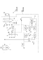
図4は、本発明の実施の形態2に係る電源装置の回路構成図である。なお、この図において前述した図1と共通する部分には同一の符号を付けている。図4において、本実施の形態の電源装置20は、実施の形態1の電源装置1における平滑コンデンサ充電スイッチ4を低圧側に配置し、また平滑コンデンサ充電スイッチ4と抵抗5の直列回路22をバイパスするバイパススイッチ(第2のスイッチ)21を有し、さらにインバータ回路15の低圧側を直接ダイオードブリッジ2の低圧側に接続したものである。その他の構成は実施の形態1の電源装置1の構成と同様である。
(Embodiment 2)
FIG. 4 is a circuit configuration diagram of a power supply device according to
なお、上記バイパススイッチ21は第2のスイッチに対応する。また、電源装置20とランプ16は照明装置110を構成する。
The
次に、上記構成の電源装置20の動作を説明する。なお、マイコン13を構成する各回路6〜12の動作は上述した通りであるので、本実施の形態の動作説明においてはマイコン13自体を主語した記載とする。さて電源が投入されると、制御電源回路(CPS)14が動作し、マイコン13に直流電圧Vccを印加する。これによりマイコン13が動作を開始し、ダイオードブリッジ2から出力される直流電源(脈流)を取り込み、電源の周波数及びピーク電圧値を計測する。この場合、計測の周期は数100μsec程度である。電源周波数の判定は電源電圧が0V付近となる周期を検知する。また、電源電圧のピーク電圧を検出電圧の最大値から求める。電源の周波数とピーク電圧値が確定すると、0V電圧のタイミングで平滑コンデンサ充電スイッチ4をオン状態にして平滑コンデンサ3の充電を行う。
Next, the operation of the
平滑コンデンサ3の充電開始とともに平滑コンデンサ3の充電状況を計測する。この場合、計測の周期は数10μsecとする。平滑コンデンサ3の充電を開始すると、平滑コンデンサ3の充電電流のピーク値ΔVと該ピーク値に到達するまでの時間(ピーク電流到達時間)Δtを求める。充電電流のピーク値ΔVは、前述したように、平滑コンデンサ3の静電容量が小さいときは小さくなり、静電容量が大きいときは大きくなる。また、ピーク電流到達時間Δtは平滑コンデンサ3の静電容量が小さいときは早くなり、静電容量が大きいときは遅くなる。
When the smoothing
充電開始から所定に時間を経過すると、平滑コンデンサ3には充電電流は流れなくなり、ピーク値ΔVとピーク電流到達時間Δtの計測が終了する。計測終了とともに計測されたピーク値ΔVとピーク電流到達時間Δtから平滑コンデンサ3の寿命判定を行う。すなわち、ピーク値ΔVの寿命が判定基準値Vref以下で、かつピーク電流到達時間Δtが判定基準時間Tref以下であれば、平滑コンデンサ3が寿命であると判定する。平滑コンデンサ3が寿命であると判定した場合、比較回路12はインバータ起動信号ENを出力せず、インバータ回路15を停止状態にする。一方、ピーク値ΔVの寿命が判定基準値Vrefを超え、かつピーク電流到達時間Δtが判定基準時間Trefを超える場合は、平滑コンデンサ3は寿命に達していないと判定して、比較回路12はインバータ起動信号ENを出力してインバータ回路15を起動させる。また同時にバイパススイッチ21をオン状態にして、平滑コンデンサ充電スイッチ4と抵抗5の直列回路22を回路から外す。これにより、抵抗5による電力消費を削減できる。
When a predetermined time elapses from the start of charging, the charging current stops flowing through the smoothing
このように本実施の形態の電源装置20は、前述した実施の形態1の電源装置1と同様に、電源位相や電圧変化による誤差を低減でき、正確に平滑コンデンサの寿命を判定することができる。また、電源電圧0V位相から充電を開始するので、突入電流の抑制ができるので、突入電流を抑制するための専用の回路が不要となり、コストの低減が可能となる。また、マイコン13はダイオードブリッジ2からの直流電源で動作するので、専用の電源を用意する必要がない分、コストの削減が図れる。また、平滑コンデンサ3の寿命判定後に、平滑コンデンサ3の充電電流を検出するための抵抗5を回路から外すので、この抵抗5による電力消費を削減できる。
As described above, the
(実施の形態3)
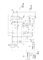
図5は、本発明の実施の形態3に係る電源装置の回路構成図である。なお、この図において前述した図1と共通する部分には同一の符号を付けている。図5において、本実施の形態の電源装置30は、上述した実施の形態1の電源装置1の構成に、通信インターフェイス31と通信線32を追加したものである。平滑コンデンサ3の寿命検知は実施の形態1の電源装置1と同様の動作であるが、検知時の制御動作が異なる。
(Embodiment 3)
FIG. 5 is a circuit configuration diagram of a power supply device according to
電源装置30のマイコン13Aは、平滑コンデンサ3の寿命を検知すると、通信インターフェイス31を介して寿命信号を通信線32に送信する。通信線32に送信された寿命信号は上位制御装置40に受信される。上位制御装置40は、他の電源装置30からの寿命信号も受信する。上位制御装置40は、寿命信号を受信すると、該信号を送信した電源装置30のマイコン13Aのテストを行う。テスト内容はマイコン13AのROMチェックサムなどである。テストが正常である場合は電源装置30の稼動時間を確認する。ここで、電源装置30のマイコン13AがEEPROM(Electrically Erasable and Programmable Read Only Memory)などの記憶媒体を備える場合、マイコン13Aは、当該記憶媒体に記憶されている稼働時間を上位制御装置40に送信する。
When detecting the life of the smoothing
上位制御装置40は、電源装置30の稼動時間が寿命となる稼働時間範囲内にある場合、その電源装置30が寿命であると判定する。そして、寿命となった電源装置30に対して出力低下などの制御を行う。また、寿命となった電源装置30の交換要求をユーザに対して報知する。
When the operating time of the
なお、本実施の形態の電源装置30とランプ16は照明装置120を構成する。
Note that the
このように本実施の形態の電源装置30は、電源装置単体での寿命検知動作ではなく、上位制御装置40でマイコン動作確認しながら寿命検知を確定することで正確な寿命判定と利便性の高い電源装置を実現できる。
As described above, the
1、20、30 電源装置
2 ダイオードブリッジ
3 平滑コンデンサ
4 平滑コンデンサ充電スイッチ
5 抵抗
6 平滑コンデンサ電流検出回路
7 入力電源電圧検出回路
8 充電開始信号出力回路
9 充電制御回路
10 ピーク電流・時間検出回路
11 基準電圧発生回路
12 比較回路
13、13A マイクロコンピュータ
14 制御電源回路
15 インバータ回路
16 ランプ
21 バイパススイッチ
22 直列回路
31 通信インターフェイス
32 通信線
40 上位制御装置
100、110、120 照明装置
DESCRIPTION OF
Claims (7)
前記整流器から出力される直流電源を平滑して直流電圧を出力する平滑コンデンサと、
前記交流電源の周波数及びピーク電圧値を計測する電源計測手段と、
前記電源計測手段による計測に基づき、0V電圧のタイミングで前記平滑コンデンサに充電を行う充電制御手段と、
前記平滑コンデンサの充電時における充電電流を検出する充電電流検出手段と、
前記充電電流検出手段で検出された充電開始直後の前記平滑コンデンサへの突入電流特性から前記平滑コンデンサの寿命を判定する平滑コンデンサ寿命判定手段と、
を備えた電源装置。 A rectifier for rectifying the AC power supply;
A smoothing capacitor for smoothing the DC power output from the rectifier and outputting a DC voltage;
Power supply measuring means for measuring the frequency and peak voltage value of the AC power supply;
Charging control means for charging the smoothing capacitor at a timing of 0 V voltage based on measurement by the power supply measuring means;
Charging current detecting means for detecting a charging current at the time of charging the smoothing capacitor;
Smoothing capacitor life determination means for determining the life of the smoothing capacitor from the inrush current characteristics to the smoothing capacitor immediately after the start of charging detected by the charging current detection means;
Power supply unit with
前記直列回路と並列に介挿される第2のスイッチと、を備え、
前記充電制御手段は、0V電圧のタイミングで前記直列回路の前記第1のスイッチをオン状態にして前記平滑コンデンサに充電を行い、前記平滑コンデンサへの充電が完了すると前記第2のスイッチをオンする請求項1に記載の電源装置。 A series circuit including a first switch and a resistor inserted in series between the output terminal of the rectifier and the smoothing capacitor;
A second switch interposed in parallel with the series circuit,
The charging control means turns on the first switch of the series circuit at a timing of 0 V voltage to charge the smoothing capacitor, and turns on the second switch when the charging to the smoothing capacitor is completed. The power supply device according to claim 1.
前記交流電源の周波数及びピーク電圧値を計測する電源計測ステップと、
前記電源計測ステップによる計測に基づき、0V電圧のタイミングで前記平滑コンデンサに充電を行う充電ステップと、
前記平滑コンデンサの充電時における充電電流を検出する充電電流検出ステップと、
前記充電電流検出ステップで検出された充電開始直後の前記平滑コンデンサへの突入電流特性から前記平滑コンデンサの寿命を判定する平滑コンデンサ寿命判定ステップと、
を備えたコンデンサ寿命判定方法。 A capacitor life determination method for determining the life of the smoothing capacitor in a power supply device including a smoothing capacitor that smoothes a DC power output from a rectifier that rectifies an AC power supply and outputs a DC voltage,
A power source measuring step for measuring the frequency and peak voltage value of the AC power source;
A charging step of charging the smoothing capacitor at a timing of 0 V voltage based on the measurement by the power source measurement step;
A charging current detection step for detecting a charging current during charging of the smoothing capacitor;
A smoothing capacitor life determination step for determining a life of the smoothing capacitor from an inrush current characteristic to the smoothing capacitor immediately after the start of charging detected in the charging current detection step;
Capacitor life judgment method with
Priority Applications (1)
| Application Number | Priority Date | Filing Date | Title |
|---|---|---|---|
| JP2009262922A JP2011106987A (en) | 2009-11-18 | 2009-11-18 | Electricity source and method for determining useful life of capacitor |
Applications Claiming Priority (1)
| Application Number | Priority Date | Filing Date | Title |
|---|---|---|---|
| JP2009262922A JP2011106987A (en) | 2009-11-18 | 2009-11-18 | Electricity source and method for determining useful life of capacitor |
Publications (1)
| Publication Number | Publication Date |
|---|---|
| JP2011106987A true JP2011106987A (en) | 2011-06-02 |
Family
ID=44230631
Family Applications (1)
| Application Number | Title | Priority Date | Filing Date |
|---|---|---|---|
| JP2009262922A Withdrawn JP2011106987A (en) | 2009-11-18 | 2009-11-18 | Electricity source and method for determining useful life of capacitor |
Country Status (1)
| Country | Link |
|---|---|
| JP (1) | JP2011106987A (en) |
Cited By (5)
| Publication number | Priority date | Publication date | Assignee | Title |
|---|---|---|---|---|
| JP2014212634A (en) * | 2013-04-18 | 2014-11-13 | 日本電信電話株式会社 | Simple deterioration determination method and simple deterioration determination device of power supply device |
| JP2018160989A (en) * | 2017-03-23 | 2018-10-11 | 東日本旅客鉄道株式会社 | Deterioration detection apparatus for electric power supply and deterioration detection method |
| JP2018170255A (en) * | 2017-03-30 | 2018-11-01 | パナソニックIpマネジメント株式会社 | Lighting device, vehicle headlamp, and vehicle |
| US10868487B2 (en) | 2017-12-27 | 2020-12-15 | Denso Corporation | Motor drive device configured to detect capacitor deterioration and to restrict a motor based upon the detected deterioration |
| JP2023503808A (en) * | 2019-11-05 | 2023-02-01 | ダタン・エヌエックスピー・セミコンダクターズ・カンパニー・リミテッド | Detection circuit and integrated circuit |
-
2009
- 2009-11-18 JP JP2009262922A patent/JP2011106987A/en not_active Withdrawn
Cited By (6)
| Publication number | Priority date | Publication date | Assignee | Title |
|---|---|---|---|---|
| JP2014212634A (en) * | 2013-04-18 | 2014-11-13 | 日本電信電話株式会社 | Simple deterioration determination method and simple deterioration determination device of power supply device |
| JP2018160989A (en) * | 2017-03-23 | 2018-10-11 | 東日本旅客鉄道株式会社 | Deterioration detection apparatus for electric power supply and deterioration detection method |
| JP2018170255A (en) * | 2017-03-30 | 2018-11-01 | パナソニックIpマネジメント株式会社 | Lighting device, vehicle headlamp, and vehicle |
| US10868487B2 (en) | 2017-12-27 | 2020-12-15 | Denso Corporation | Motor drive device configured to detect capacitor deterioration and to restrict a motor based upon the detected deterioration |
| JP2023503808A (en) * | 2019-11-05 | 2023-02-01 | ダタン・エヌエックスピー・セミコンダクターズ・カンパニー・リミテッド | Detection circuit and integrated circuit |
| JP7431324B2 (en) | 2019-11-05 | 2024-02-14 | 大唐恩智浦半導体有限公司 | Detection circuits and integrated circuits |
Similar Documents
| Publication | Publication Date | Title |
|---|---|---|
| TWI479784B (en) | AC to DC conversion circuit | |
| US8488339B2 (en) | Switching power supply | |
| KR100930813B1 (en) | Active Constant Power Supply | |
| RU2665463C2 (en) | Driver device and driving method for driving load, in particular in led unit comprising one or more leds | |
| US20110210712A1 (en) | AC or DC POWER SUPPLY EMPLOYING SAMPLING POWER CIRCUIT | |
| CN108243545B (en) | Load control device | |
| TWI686042B (en) | Power conversion device | |
| CN112462127B (en) | Surge current testing device | |
| JP6032749B2 (en) | Switching power supply | |
| JP2011106987A (en) | Electricity source and method for determining useful life of capacitor | |
| CN111090016A (en) | Silicon controlled rectifier dimmer detection device, circuit and detection method thereof | |
| CN105450054A (en) | PFC (power factor correction) circuit with built-in auxiliary power circuit, and control method and device for PFC circuit | |
| WO2012014086A2 (en) | Method and apparatus for wave detection | |
| TW201218605A (en) | AC/DC converter, AC/DC conversion method, and controller for controlling voltage conversion | |
| CN102299617A (en) | Automatic voltage switch and implementation method thereof | |
| JP2011109823A (en) | Power supply apparatus and method for determining capacitor life | |
| JP2016201934A (en) | Deterioration detection device and deterioration detection method of power supply device | |
| CN101741263A (en) | Insulated switch power supply apparatus | |
| JP2011108518A (en) | Discharge lamp lighting device and capacitor life end determining method | |
| TWM579758U (en) | Electronic device | |
| JP7167843B2 (en) | car charger | |
| JP2014171297A (en) | Power conditioner | |
| JP2011050120A (en) | Power converter | |
| JP2005192353A (en) | Power supply anomaly detector and power supply device using the same | |
| JP2016217775A (en) | Commercial ac power source cutoff detection device, equipment system with the same, and image formation device |
Legal Events
| Date | Code | Title | Description |
|---|---|---|---|
| A711 | Notification of change in applicant |
Free format text: JAPANESE INTERMEDIATE CODE: A712 Effective date: 20120116 |
|
| A300 | Application deemed to be withdrawn because no request for examination was validly filed |
Free format text: JAPANESE INTERMEDIATE CODE: A300 Effective date: 20130205 |