JP2011108252A - メモリカード及びデータ処理装置並びにメモリカードの制御方法及び設定方法 - Google Patents
メモリカード及びデータ処理装置並びにメモリカードの制御方法及び設定方法 Download PDFInfo
- Publication number
- JP2011108252A JP2011108252A JP2010285813A JP2010285813A JP2011108252A JP 2011108252 A JP2011108252 A JP 2011108252A JP 2010285813 A JP2010285813 A JP 2010285813A JP 2010285813 A JP2010285813 A JP 2010285813A JP 2011108252 A JP2011108252 A JP 2011108252A
- Authority
- JP
- Japan
- Prior art keywords
- memory card
- error correction
- data
- read
- memory
- Prior art date
- Legal status (The legal status is an assumption and is not a legal conclusion. Google has not performed a legal analysis and makes no representation as to the accuracy of the status listed.)
- Granted
Links
Images



Classifications
-
- G—PHYSICS
- G06—COMPUTING OR CALCULATING; COUNTING
- G06F—ELECTRIC DIGITAL DATA PROCESSING
- G06F13/00—Interconnection of, or transfer of information or other signals between, memories, input/output devices or central processing units
- G06F13/38—Information transfer, e.g. on bus
- G06F13/382—Information transfer, e.g. on bus using universal interface adapter
- G06F13/385—Information transfer, e.g. on bus using universal interface adapter for adaptation of a particular data processing system to different peripheral devices
-
- G—PHYSICS
- G06—COMPUTING OR CALCULATING; COUNTING
- G06F—ELECTRIC DIGITAL DATA PROCESSING
- G06F11/00—Error detection; Error correction; Monitoring
- G06F11/07—Responding to the occurrence of a fault, e.g. fault tolerance
- G06F11/0703—Error or fault processing not based on redundancy, i.e. by taking additional measures to deal with the error or fault not making use of redundancy in operation, in hardware, or in data representation
- G06F11/0706—Error or fault processing not based on redundancy, i.e. by taking additional measures to deal with the error or fault not making use of redundancy in operation, in hardware, or in data representation the processing taking place on a specific hardware platform or in a specific software environment
- G06F11/073—Error or fault processing not based on redundancy, i.e. by taking additional measures to deal with the error or fault not making use of redundancy in operation, in hardware, or in data representation the processing taking place on a specific hardware platform or in a specific software environment in a memory management context, e.g. virtual memory or cache management
-
- G—PHYSICS
- G06—COMPUTING OR CALCULATING; COUNTING
- G06F—ELECTRIC DIGITAL DATA PROCESSING
- G06F11/00—Error detection; Error correction; Monitoring
- G06F11/07—Responding to the occurrence of a fault, e.g. fault tolerance
- G06F11/08—Error detection or correction by redundancy in data representation, e.g. by using checking codes
- G06F11/10—Adding special bits or symbols to the coded information, e.g. parity check, casting out 9's or 11's
- G06F11/1008—Adding special bits or symbols to the coded information, e.g. parity check, casting out 9's or 11's in individual solid state devices
- G06F11/1048—Adding special bits or symbols to the coded information, e.g. parity check, casting out 9's or 11's in individual solid state devices using arrangements adapted for a specific error detection or correction feature
- G06F11/1052—Bypassing or disabling error detection or correction
-
- G—PHYSICS
- G06—COMPUTING OR CALCULATING; COUNTING
- G06F—ELECTRIC DIGITAL DATA PROCESSING
- G06F11/00—Error detection; Error correction; Monitoring
- G06F11/07—Responding to the occurrence of a fault, e.g. fault tolerance
- G06F11/0703—Error or fault processing not based on redundancy, i.e. by taking additional measures to deal with the error or fault not making use of redundancy in operation, in hardware, or in data representation
- G06F11/0793—Remedial or corrective actions
-
- G—PHYSICS
- G11—INFORMATION STORAGE
- G11C—STATIC STORES
- G11C29/00—Checking stores for correct operation ; Subsequent repair; Testing stores during standby or offline operation
- G11C29/04—Detection or location of defective memory elements, e.g. cell constructio details, timing of test signals
- G11C2029/0409—Online test
Landscapes
- Engineering & Computer Science (AREA)
- Theoretical Computer Science (AREA)
- Physics & Mathematics (AREA)
- General Engineering & Computer Science (AREA)
- General Physics & Mathematics (AREA)
- Quality & Reliability (AREA)
- Techniques For Improving Reliability Of Storages (AREA)
Abstract
【解決手段】メモリカードは、データ処理装置との間でコマンドやデータの送受信を行うホストインタフェース(2)と、データを格納する不揮発性メモリ(7)と、メモリカードの動作を制御するコントローラ(3)と、所定の管理情報を格納する記憶手段(32)とを備える。管理情報は、不揮発性メモリからのデータの読み出し時に誤り訂正機能を実行するか否かを指定するための誤り訂正設定情報を含む。コントローラは、データ読み出し動作時に、誤り訂正設定情報を参照し、誤り訂正設定情報が誤り訂正機能の停止を示す場合は、読み出したデータに対して誤り訂正を行わないように、また、誤り訂正設定情報が誤り訂正機能の作動を示す場合は、読み出したデータに対して誤り訂正を行うように、読み出し動作を制御する。
【選択図】図1
Description
コントローラは、メモリカードがデータ処理装置に装着されたとき又はデータ処理装置の電源投入時に、メモリカードから特性情報を読み出し、読み出した特性情報に基づき、メモリカードにおいてリトライ機能を実行させるか否かの判断を行い、その判断結果にしたがい、リトライ設定情報を設定するためのコマンドをカードインタフェースを介してメモリカードに送信する。
管理情報は、不揮発性メモリからのデータの読み出し時に誤り訂正機能を実行するか否かを指定するための誤り訂正設定情報を含む。
コントローラは、データ読み出し動作時に、誤り訂正設定情報を参照し、誤り訂正設定情報が誤り訂正機能の停止を示す場合は、読み出したデータに対して誤り訂正を行わないように、また、誤り訂正設定情報が誤り訂正機能の作動を示す場合は、読み出したデータに対して誤り訂正を行うように、読み出し動作を制御する。
特性情報は、不揮発性メモリの誤り率に関する情報を含んでもよい。
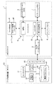
ホスト(データ処理装置)50は、例えばディジタルスチルカメラ、ディジタルビデオカメラ、各種携帯端末機器、パーソナルコンピュータ等の電子機器を含む。
メモリカード1はホスト50に装着されて使用され、ホスト50からデータの書き込み、読み出しが可能な記録媒体である。メモリカード1は、書き込み時にエラーが生じたときに再試行するリトライ機能と、データの誤り訂正を行う誤り訂正機能とを有する。
図4に示すフローチャートを参照し、ホスト50がメモリカード1の初期化時に行う処理について説明する。図4に示す処理は、ホスト50のコントローラ51により実行され、メモリカード1がホスト50に新たに装着されたときや、メモリカード1が装着された状態でホスト50の電源が投入された時等に実行される。
判定条件1: リトライ発生頻度×リトライ処理を行う場合の書き込み時間の最大所要時間
判定条件2: エラー発生頻度×リトライ処理を行わない場合の書き込み時間の最大所要時間
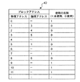
メモリカード1のデータ書き込み処理について、図5に示すフローチャートを参照して説明する。図5に示すフローチャートは、メモリカード1のコントローラ3により実行される。また、本処理はメモリカード1がホスト50から書き込みコマンドを受信したときに開始される。なお、以下では説明の便宜上、フラッシュメモリ7におけるデータ書き込み単位であるページとデータ消去単位であるブロックとを同じサイズに設定している。よって、データはブロック単位で書き込まれる。
次にメモリカード1のデータ読み出し処理について、図6に示すフローチャートを参照して説明する。図6に示される処理は、コントローラ3により実行されるものである。また、本処理はメモリカード1がホスト50から読み出しコマンドを受信したときに開始される。
2 ホストインタフェース
3 コントローラ
4 RAM
5 インストラクションROM
6 バッファメモリ
7 フラッシュメモリ
31 マイクロプロセッサ(MPU)
32 レジスタ
33 誤り訂正手段
41 ワークRAM
42 ブロック管理テーブル
50 ホスト(データ処理装置)
51 コントローラ
53 データ格納部
55 カードインタフェース
57 入出力処理部
59 バッファメモリ
Claims (5)
- データ処理装置からデータの書き込み、読み出しが可能なメモリカードであって、
データ処理装置との間でコマンドやデータの送受信を行うホストインタフェースと、
データを格納する不揮発性メモリと、
メモリカードの動作を制御するコントローラと、
所定の管理情報を格納する記憶手段とを備え、
前記管理情報は、不揮発性メモリからのデータの読み出し時に誤り訂正機能を実行するか否かを指定するための誤り訂正設定情報を含み、
前記コントローラは、データ読み出し動作時に、誤り訂正設定情報を参照し、誤り訂正設定情報が誤り訂正機能の停止を示す場合は、読み出したデータに対して誤り訂正を行わないように、また、誤り訂正設定情報が誤り訂正機能の作動を示す場合は、読み出したデータに対して誤り訂正を行うように、読み出し動作を制御する、
メモリカード。 - 前記管理情報はさらにメモリカード固有の特性情報を含み、前記コントローラは前記データ処理装置からの要求に応じて前記特性情報をデータ処理装置に送信する、
請求項1記載のメモリカード。 - データの読み出し、書き込みが可能で、かつ、読み出したデータに対して誤り訂正を実行可能なメモリカードであって、読み出し動作時に誤り訂正機能を実行するか否かを指定するための誤り訂正設定情報及びメモリカード固有の特性情報を管理情報として格納するメモリカードにアクセス可能なデータ処理装置であって、
メモリカードとの間でコマンドやデータの送受信を行うカードインタフェースと、
データ処理装置の動作を制御するコントローラとを備え、
前記コントローラは、メモリカードがデータ処理装置に装着されたとき又はデータ処理装置の電源投入時に、メモリカードから特性情報を読み出し、読み出した特性情報に基づき、メモリカードにおいて誤り訂正機能を実行するか否かの判断を行い、その判断結果にしたがい、誤り訂正設定情報を設定するためのコマンドをカードインタフェースを介してメモリカードに送信する、
データ処理装置。 - データの書き込み、読み出しが可能で、かつ、読み出したデータに対して誤り訂正を実行可能なメモリカードであって、読み出し動作時に誤り訂正機能を実行するか否かを指定するための誤り訂正設定情報を管理情報として格納するメモリカードの制御方法であって、
データ読み出し動作時に、誤り訂正設定情報を参照し、
誤り訂正設定情報が誤り訂正機能の停止を示す場合は、読み出したデータに対して誤り訂正を行わず、
一方、誤り訂正設定情報が誤り訂正機能の作動を示す場合は、読み出したデータに対して誤り訂正を行う、
メモリカードの制御方法。 - データの読み出し、書き込みが可能で、かつ、読み出したデータに対して誤り訂正を実行可能なメモリカードであって、読み出し動作時に誤り訂正機能を実行するか否かを指定するための誤り訂正設定情報及びメモリカード固有の特性情報を管理情報として格納するメモリカードに対する設定方法であって、
前記メモリカードから特性情報を読み出し、読み出した特性情報に基づいて、メモリカードにおいて誤り訂正機能を実行するか否かの判断を行い、その判断結果にしたがい、誤り訂正設定情報を設定するためのコマンドをカードインタフェースを介してメモリカードに送信する、
メモリカードに対する設定方法。
Priority Applications (1)
| Application Number | Priority Date | Filing Date | Title |
|---|---|---|---|
| JP2010285813A JP5079868B2 (ja) | 2004-02-03 | 2010-12-22 | メモリカード及びデータ処理装置並びにメモリカードの制御方法及び設定方法 |
Applications Claiming Priority (3)
| Application Number | Priority Date | Filing Date | Title |
|---|---|---|---|
| JP2004026413 | 2004-02-03 | ||
| JP2004026413 | 2004-02-03 | ||
| JP2010285813A JP5079868B2 (ja) | 2004-02-03 | 2010-12-22 | メモリカード及びデータ処理装置並びにメモリカードの制御方法及び設定方法 |
Related Parent Applications (1)
| Application Number | Title | Priority Date | Filing Date |
|---|---|---|---|
| JP2005517700A Division JP4679370B2 (ja) | 2004-02-03 | 2005-02-02 | データ処理装置並びにメモリカードの設定方法 |
Publications (2)
| Publication Number | Publication Date |
|---|---|
| JP2011108252A true JP2011108252A (ja) | 2011-06-02 |
| JP5079868B2 JP5079868B2 (ja) | 2012-11-21 |
Family
ID=34835848
Family Applications (2)
| Application Number | Title | Priority Date | Filing Date |
|---|---|---|---|
| JP2005517700A Expired - Fee Related JP4679370B2 (ja) | 2004-02-03 | 2005-02-02 | データ処理装置並びにメモリカードの設定方法 |
| JP2010285813A Expired - Fee Related JP5079868B2 (ja) | 2004-02-03 | 2010-12-22 | メモリカード及びデータ処理装置並びにメモリカードの制御方法及び設定方法 |
Family Applications Before (1)
| Application Number | Title | Priority Date | Filing Date |
|---|---|---|---|
| JP2005517700A Expired - Fee Related JP4679370B2 (ja) | 2004-02-03 | 2005-02-02 | データ処理装置並びにメモリカードの設定方法 |
Country Status (4)
| Country | Link |
|---|---|
| US (1) | US7624298B2 (ja) |
| JP (2) | JP4679370B2 (ja) |
| CN (1) | CN100535933C (ja) |
| WO (1) | WO2005076203A1 (ja) |
Cited By (4)
| Publication number | Priority date | Publication date | Assignee | Title |
|---|---|---|---|---|
| JP2015518994A (ja) * | 2012-06-07 | 2015-07-06 | マイクロン テクノロジー, インク. | アドレスバスの完全性の改善 |
| US9323608B2 (en) | 2012-06-07 | 2016-04-26 | Micron Technology, Inc. | Integrity of a data bus |
| JP2018101834A (ja) * | 2016-12-19 | 2018-06-28 | 京セラドキュメントソリューションズ株式会社 | 画像形成装置、及び画像形成システム |
| KR20190113080A (ko) * | 2018-03-27 | 2019-10-08 | 삼성전자주식회사 | 메모리 모듈을 포함하는 메모리 시스템, 메모리 모듈, 그리고 메모리 모듈의 동작 방법 |
Families Citing this family (28)
| Publication number | Priority date | Publication date | Assignee | Title |
|---|---|---|---|---|
| JP4871260B2 (ja) * | 2005-03-03 | 2012-02-08 | パナソニック株式会社 | メモリモジュール、メモリコントローラ、不揮発性記憶装置、不揮発性記憶システム、及びメモリの読み書き方法 |
| US9459960B2 (en) | 2005-06-03 | 2016-10-04 | Rambus Inc. | Controller device for use with electrically erasable programmable memory chip with error detection and retry modes of operation |
| US7831882B2 (en) | 2005-06-03 | 2010-11-09 | Rambus Inc. | Memory system with error detection and retry modes of operation |
| US8291295B2 (en) | 2005-09-26 | 2012-10-16 | Sandisk Il Ltd. | NAND flash memory controller exporting a NAND interface |
| WO2007049455A1 (ja) * | 2005-10-28 | 2007-05-03 | Matsushita Electric Industrial Co., Ltd. | 半導体メモリカード |
| US7562285B2 (en) | 2006-01-11 | 2009-07-14 | Rambus Inc. | Unidirectional error code transfer for a bidirectional data link |
| US8352805B2 (en) | 2006-05-18 | 2013-01-08 | Rambus Inc. | Memory error detection |
| US20070271495A1 (en) * | 2006-05-18 | 2007-11-22 | Ian Shaeffer | System to detect and identify errors in control information, read data and/or write data |
| US7809899B2 (en) * | 2007-05-29 | 2010-10-05 | Lsi Corporation | System for integrity protection for standard 2n-bit multiple sized memory devices |
| CN101354754B (zh) * | 2007-07-26 | 2011-03-16 | 上海瀚银信息技术有限公司 | 一种内嵌cpu ic的智能存储卡及其应用 |
| US8443260B2 (en) * | 2007-12-27 | 2013-05-14 | Sandisk Il Ltd. | Error correction in copy back memory operations |
| JP2009252036A (ja) * | 2008-04-08 | 2009-10-29 | Panasonic Corp | メモリカード |
| US9594679B2 (en) * | 2008-05-01 | 2017-03-14 | Sandisk Il Ltd. | Flash cache flushing method and system |
| JP5404804B2 (ja) * | 2009-05-25 | 2014-02-05 | 株式会社日立製作所 | ストレージサブシステム |
| TWI416523B (zh) * | 2009-06-10 | 2013-11-21 | Silicon Motion Inc | 非揮發性記憶體之寫入錯誤管理方法、非揮發性記憶體、記憶卡、以及非揮發性記憶體之控制器 |
| US20110041005A1 (en) * | 2009-08-11 | 2011-02-17 | Selinger Robert D | Controller and Method for Providing Read Status and Spare Block Management Information in a Flash Memory System |
| TWI424435B (zh) | 2009-08-31 | 2014-01-21 | Phison Electronics Corp | 對快閃記憶體下達程式化指令的方法、控制器與儲存系統 |
| CN102023811B (zh) * | 2009-09-10 | 2012-11-28 | 群联电子股份有限公司 | 对闪存下达程序化指令的方法和系统 |
| KR101279710B1 (ko) * | 2011-04-01 | 2013-06-27 | 엘에스산전 주식회사 | Plc 데이터 로그모듈 및 이의 데이터 저장 방법 |
| US8656251B2 (en) * | 2011-09-02 | 2014-02-18 | Apple Inc. | Simultaneous data transfer and error control to reduce latency and improve throughput to a host |
| CN104718578A (zh) | 2012-12-21 | 2015-06-17 | 惠普发展公司,有限责任合伙企业 | 具有错误校正逻辑的存储模块 |
| JP6184121B2 (ja) * | 2013-02-08 | 2017-08-23 | 株式会社メガチップス | 記憶装置検査システム、記憶装置検査方法および不揮発性半導体記憶装置 |
| CN103546638B (zh) * | 2013-10-29 | 2016-02-03 | 广东欧珀移动通信有限公司 | 一种快闪存储卡的掉卡恢复方法及其移动终端 |
| EP3776207B1 (en) | 2018-03-26 | 2023-08-09 | Rambus Inc. | Command/address channel error detection |
| US10990463B2 (en) | 2018-03-27 | 2021-04-27 | Samsung Electronics Co., Ltd. | Semiconductor memory module and memory system including the same |
| US10691377B2 (en) | 2018-09-21 | 2020-06-23 | Micron Technology, Inc. | Adjusting scan event thresholds to mitigate memory errors |
| US11537464B2 (en) | 2019-06-14 | 2022-12-27 | Micron Technology, Inc. | Host-based error correction |
| JP7752333B2 (ja) * | 2022-05-30 | 2025-10-10 | パナソニックIpマネジメント株式会社 | データ記録システム、ストレージ、及び、ストレージの制御方法 |
Citations (2)
| Publication number | Priority date | Publication date | Assignee | Title |
|---|---|---|---|---|
| JPH01209552A (ja) * | 1988-02-17 | 1989-08-23 | Hitachi Maxell Ltd | 半導体ファイルメモリ装置 |
| JPH0728690A (ja) * | 1993-07-14 | 1995-01-31 | Hitachi Ltd | フラッシュメモリシステム |
Family Cites Families (15)
| Publication number | Priority date | Publication date | Assignee | Title |
|---|---|---|---|---|
| US4706190A (en) * | 1983-09-22 | 1987-11-10 | Digital Equipment Corporation | Retry mechanism for releasing control of a communications path in digital computer system |
| US5369532A (en) * | 1991-11-12 | 1994-11-29 | Storage Technology Corporation | Method and apparatus for managing data on rewritable media to define read/write operational status |
| US5828583A (en) * | 1992-08-21 | 1998-10-27 | Compaq Computer Corporation | Drive failure prediction techniques for disk drives |
| KR970008188B1 (ko) | 1993-04-08 | 1997-05-21 | 가부시끼가이샤 히다찌세이사꾸쇼 | 플래시메모리의 제어방법 및 그것을 사용한 정보처리장치 |
| US6078520A (en) | 1993-04-08 | 2000-06-20 | Hitachi, Ltd. | Flash memory control method and information processing system therewith |
| JPH0714392A (ja) * | 1993-06-14 | 1995-01-17 | Toshiba Corp | 不揮発性半導体メモリおよびそれを使用した半導体ディスク装置 |
| JP3576625B2 (ja) | 1995-02-28 | 2004-10-13 | 株式会社東芝 | フラッシュメモリカードのデータ管理方法およびそのデータ管理方法を使用したデータ処理装置 |
| JP3242890B2 (ja) | 1998-12-16 | 2001-12-25 | 株式会社ハギワラシスコム | 記憶装置 |
| JP4031190B2 (ja) * | 2000-09-29 | 2008-01-09 | 株式会社東芝 | メモリカード、不揮発性メモリ、不揮発性メモリのデータ書き込み方法及びデータ書き込み装置 |
| WO2002058296A2 (en) * | 2001-01-17 | 2002-07-25 | Broadcom Corporation | System and method for a guaranteed delay jitter bound when scheduling bandwidth grants for voice calls via a cable network |
| JP4173297B2 (ja) * | 2001-09-13 | 2008-10-29 | 株式会社ルネサステクノロジ | メモリカード |
| US7076604B1 (en) * | 2002-12-24 | 2006-07-11 | Western Digital Technologies, Inc. | Disk drive employing a disk command data structure for tracking a write verify status of a write command |
| US7177989B1 (en) * | 2003-12-31 | 2007-02-13 | Intel Corporation | Retry of a device read transaction |
| WO2006033156A1 (ja) * | 2004-09-24 | 2006-03-30 | Renesas Technology Corp. | 半導体装置 |
| JP2006209525A (ja) | 2005-01-28 | 2006-08-10 | Matsushita Electric Ind Co Ltd | メモリシステム |
-
2005
- 2005-02-02 WO PCT/JP2005/001496 patent/WO2005076203A1/ja not_active Ceased
- 2005-02-02 US US10/597,650 patent/US7624298B2/en not_active Expired - Fee Related
- 2005-02-02 CN CNB2005800039528A patent/CN100535933C/zh not_active Expired - Fee Related
- 2005-02-02 JP JP2005517700A patent/JP4679370B2/ja not_active Expired - Fee Related
-
2010
- 2010-12-22 JP JP2010285813A patent/JP5079868B2/ja not_active Expired - Fee Related
Patent Citations (2)
| Publication number | Priority date | Publication date | Assignee | Title |
|---|---|---|---|---|
| JPH01209552A (ja) * | 1988-02-17 | 1989-08-23 | Hitachi Maxell Ltd | 半導体ファイルメモリ装置 |
| JPH0728690A (ja) * | 1993-07-14 | 1995-01-31 | Hitachi Ltd | フラッシュメモリシステム |
Cited By (7)
| Publication number | Priority date | Publication date | Assignee | Title |
|---|---|---|---|---|
| JP2015518994A (ja) * | 2012-06-07 | 2015-07-06 | マイクロン テクノロジー, インク. | アドレスバスの完全性の改善 |
| US9323608B2 (en) | 2012-06-07 | 2016-04-26 | Micron Technology, Inc. | Integrity of a data bus |
| US9557926B2 (en) | 2012-06-07 | 2017-01-31 | Micron Technology, Inc. | Integrity of an address bus |
| US9639422B2 (en) | 2012-06-07 | 2017-05-02 | Micron Technology, Inc. | Synchronized transfer of data and corresponding error correction data |
| US10152373B2 (en) | 2012-06-07 | 2018-12-11 | Micron Technology, Inc. | Methods of operating memory including receipt of ECC data |
| JP2018101834A (ja) * | 2016-12-19 | 2018-06-28 | 京セラドキュメントソリューションズ株式会社 | 画像形成装置、及び画像形成システム |
| KR20190113080A (ko) * | 2018-03-27 | 2019-10-08 | 삼성전자주식회사 | 메모리 모듈을 포함하는 메모리 시스템, 메모리 모듈, 그리고 메모리 모듈의 동작 방법 |
Also Published As
| Publication number | Publication date |
|---|---|
| JP4679370B2 (ja) | 2011-04-27 |
| WO2005076203A1 (ja) | 2005-08-18 |
| JPWO2005076203A1 (ja) | 2007-10-18 |
| CN1914627A (zh) | 2007-02-14 |
| US7624298B2 (en) | 2009-11-24 |
| JP5079868B2 (ja) | 2012-11-21 |
| CN100535933C (zh) | 2009-09-02 |
| US20070186040A1 (en) | 2007-08-09 |
Similar Documents
| Publication | Publication Date | Title |
|---|---|---|
| JP5079868B2 (ja) | メモリカード及びデータ処理装置並びにメモリカードの制御方法及び設定方法 | |
| US7596041B2 (en) | Nonvolatile memory system | |
| EP2162822B1 (en) | Emerging bad block detection | |
| JP4110000B2 (ja) | 記憶装置 | |
| US11138080B2 (en) | Apparatus and method for reducing cell disturb in an open block of a memory system during a recovery procedure | |
| JP3233079B2 (ja) | データ処理システム及びデータ処理方法 | |
| US9164833B2 (en) | Data storage device, operating method thereof and data processing system including the same | |
| KR20190022987A (ko) | 데이터 저장 장치 및 그것의 동작 방법 | |
| US11068177B2 (en) | Data storage devices and data processing methods for shortening time required for a host device to wait for initialization of the data storage device | |
| US10083114B2 (en) | Data storage device and operating method thereof | |
| KR102444606B1 (ko) | 데이터 저장 장치 및 그것의 동작 방법 | |
| JP2004220068A (ja) | メモリカード及びメモリへのデータ書き込み方法 | |
| US8489802B2 (en) | Recordable memory device which writes data to reformatted user area of nonvolatile semiconductor memory | |
| KR20200019513A (ko) | 컨트롤러, 메모리 시스템 및 그 동작 방법 | |
| US8151136B2 (en) | Method and device for correcting code data error | |
| JP3620478B2 (ja) | 記憶装置、この記憶装置を用いたデータ処理システム及びデータ読み出し方法 | |
| US8627157B2 (en) | Storing apparatus | |
| TWI779046B (zh) | 記憶體裝置及包括其的記憶體系統 | |
| JP2009176147A (ja) | 電子機器および電子機器のメモリアクセス許可判別方法 | |
| US11467910B2 (en) | Memory system re-performing access operation and operating method thereof | |
| CN109933282B (zh) | 存储器系统及其操作方法 | |
| US20230214151A1 (en) | Memory system and operating method thereof | |
| JP3444988B2 (ja) | 不揮発性半導体ディスク装置およびその制御方法 | |
| JP2010079371A (ja) | 記憶装置及び電子機器 | |
| JP2005234928A (ja) | 記憶装置 |
Legal Events
| Date | Code | Title | Description |
|---|---|---|---|
| A131 | Notification of reasons for refusal |
Free format text: JAPANESE INTERMEDIATE CODE: A131 Effective date: 20120605 |
|
| A521 | Request for written amendment filed |
Free format text: JAPANESE INTERMEDIATE CODE: A523 Effective date: 20120802 |
|
| TRDD | Decision of grant or rejection written | ||
| A01 | Written decision to grant a patent or to grant a registration (utility model) |
Free format text: JAPANESE INTERMEDIATE CODE: A01 Effective date: 20120821 |
|
| A01 | Written decision to grant a patent or to grant a registration (utility model) |
Free format text: JAPANESE INTERMEDIATE CODE: A01 |
|
| A61 | First payment of annual fees (during grant procedure) |
Free format text: JAPANESE INTERMEDIATE CODE: A61 Effective date: 20120829 |
|
| FPAY | Renewal fee payment (event date is renewal date of database) |
Free format text: PAYMENT UNTIL: 20150907 Year of fee payment: 3 |
|
| R150 | Certificate of patent or registration of utility model |
Free format text: JAPANESE INTERMEDIATE CODE: R150 |
|
| LAPS | Cancellation because of no payment of annual fees |