JP2011114031A - Ceramic package for storing electronic component - Google Patents
Ceramic package for storing electronic component Download PDFInfo
- Publication number
- JP2011114031A JP2011114031A JP2009266513A JP2009266513A JP2011114031A JP 2011114031 A JP2011114031 A JP 2011114031A JP 2009266513 A JP2009266513 A JP 2009266513A JP 2009266513 A JP2009266513 A JP 2009266513A JP 2011114031 A JP2011114031 A JP 2011114031A
- Authority
- JP
- Japan
- Prior art keywords
- ceramic
- ceramic base
- electronic component
- package
- thickness
- Prior art date
- Legal status (The legal status is an assumption and is not a legal conclusion. Google has not performed a legal analysis and makes no representation as to the accuracy of the status listed.)
- Pending
Links
- 239000000919 ceramic Substances 0.000 title claims abstract description 191
- 238000005476 soldering Methods 0.000 claims abstract description 14
- 229910000679 solder Inorganic materials 0.000 claims abstract description 12
- 239000000758 substrate Substances 0.000 claims description 64
- 239000011104 metalized film Substances 0.000 claims description 39
- 238000001465 metallisation Methods 0.000 claims description 3
- 238000005304 joining Methods 0.000 abstract description 2
- 239000010408 film Substances 0.000 description 11
- 238000003860 storage Methods 0.000 description 9
- 239000004020 conductor Substances 0.000 description 8
- 238000007747 plating Methods 0.000 description 8
- 238000010304 firing Methods 0.000 description 7
- 239000002184 metal Substances 0.000 description 7
- 229910052751 metal Inorganic materials 0.000 description 7
- 238000005520 cutting process Methods 0.000 description 6
- 239000004065 semiconductor Substances 0.000 description 6
- 238000000034 method Methods 0.000 description 4
- YXFVVABEGXRONW-UHFFFAOYSA-N Toluene Chemical compound CC1=CC=CC=C1 YXFVVABEGXRONW-UHFFFAOYSA-N 0.000 description 3
- PNEYBMLMFCGWSK-UHFFFAOYSA-N aluminium oxide Inorganic materials [O-2].[O-2].[O-2].[Al+3].[Al+3] PNEYBMLMFCGWSK-UHFFFAOYSA-N 0.000 description 3
- 239000013078 crystal Substances 0.000 description 3
- 230000005499 meniscus Effects 0.000 description 3
- 239000000843 powder Substances 0.000 description 3
- 238000004080 punching Methods 0.000 description 3
- 239000003870 refractory metal Substances 0.000 description 3
- CPLXHLVBOLITMK-UHFFFAOYSA-N Magnesium oxide Chemical compound [Mg]=O CPLXHLVBOLITMK-UHFFFAOYSA-N 0.000 description 2
- ZOKXTWBITQBERF-UHFFFAOYSA-N Molybdenum Chemical compound [Mo] ZOKXTWBITQBERF-UHFFFAOYSA-N 0.000 description 2
- VYPSYNLAJGMNEJ-UHFFFAOYSA-N Silicium dioxide Chemical compound O=[Si]=O VYPSYNLAJGMNEJ-UHFFFAOYSA-N 0.000 description 2
- 230000004308 accommodation Effects 0.000 description 2
- 238000004519 manufacturing process Methods 0.000 description 2
- 229910052750 molybdenum Inorganic materials 0.000 description 2
- 239000011733 molybdenum Substances 0.000 description 2
- 239000002002 slurry Substances 0.000 description 2
- WFKWXMTUELFFGS-UHFFFAOYSA-N tungsten Chemical compound [W] WFKWXMTUELFFGS-UHFFFAOYSA-N 0.000 description 2
- 229910052721 tungsten Inorganic materials 0.000 description 2
- 239000010937 tungsten Substances 0.000 description 2
- 239000004925 Acrylic resin Substances 0.000 description 1
- 229920000178 Acrylic resin Polymers 0.000 description 1
- 229910018072 Al 2 O 3 Inorganic materials 0.000 description 1
- PIGFYZPCRLYGLF-UHFFFAOYSA-N Aluminum nitride Chemical compound [Al]#N PIGFYZPCRLYGLF-UHFFFAOYSA-N 0.000 description 1
- ODINCKMPIJJUCX-UHFFFAOYSA-N Calcium oxide Chemical compound [Ca]=O ODINCKMPIJJUCX-UHFFFAOYSA-N 0.000 description 1
- MQIUGAXCHLFZKX-UHFFFAOYSA-N Di-n-octyl phthalate Natural products CCCCCCCCOC(=O)C1=CC=CC=C1C(=O)OCCCCCCCC MQIUGAXCHLFZKX-UHFFFAOYSA-N 0.000 description 1
- CTQNGGLPUBDAKN-UHFFFAOYSA-N O-Xylene Chemical compound CC1=CC=CC=C1C CTQNGGLPUBDAKN-UHFFFAOYSA-N 0.000 description 1
- 239000000853 adhesive Substances 0.000 description 1
- 230000001070 adhesive effect Effects 0.000 description 1
- 150000001298 alcohols Chemical class 0.000 description 1
- 239000011230 binding agent Substances 0.000 description 1
- BJQHLKABXJIVAM-UHFFFAOYSA-N bis(2-ethylhexyl) phthalate Chemical compound CCCCC(CC)COC(=O)C1=CC=CC=C1C(=O)OCC(CC)CCCC BJQHLKABXJIVAM-UHFFFAOYSA-N 0.000 description 1
- 239000000292 calcium oxide Substances 0.000 description 1
- 235000012255 calcium oxide Nutrition 0.000 description 1
- 230000001351 cycling effect Effects 0.000 description 1
- 238000007606 doctor blade method Methods 0.000 description 1
- 238000010438 heat treatment Methods 0.000 description 1
- 239000000395 magnesium oxide Substances 0.000 description 1
- 239000011159 matrix material Substances 0.000 description 1
- 239000004014 plasticizer Substances 0.000 description 1
- 238000003825 pressing Methods 0.000 description 1
- 238000007639 printing Methods 0.000 description 1
- 238000007650 screen-printing Methods 0.000 description 1
- 239000000377 silicon dioxide Substances 0.000 description 1
- 238000005245 sintering Methods 0.000 description 1
- 239000002904 solvent Substances 0.000 description 1
- 239000008096 xylene Substances 0.000 description 1
Images

Landscapes
- Piezo-Electric Or Mechanical Vibrators, Or Delay Or Filter Circuits (AREA)
Abstract
Description
本発明は、半導体素子や、発光素子や、水晶振動子等の電子部品を収納するための電子部品収納用セラミックパッケージに関し、より詳細には、電子部品をセラミック基体に収納し、このセラミック基体を立設させて実装用配線基板に搭載する電子部品収納用セラミックパッケージに関する。 The present invention relates to a ceramic package for storing an electronic component for storing an electronic component such as a semiconductor element, a light emitting element, or a crystal resonator. More specifically, the electronic component is stored in a ceramic substrate. The present invention relates to a ceramic package for storing electronic components that is erected and mounted on a wiring board for mounting.
従来から、電子部品収納用セラミックパッケージには、複数枚の大型のセラミックグリーンシートが用いられている。それぞれのセラミックグリーンシートには、複数個のセラミック基体用の孔開け加工を行った後、パッケージ内に電気的導通を形成するための導体金属ペーストによる配線をスクリーン印刷で形成している。更に、それぞれのセラミックグリーンシートは、重ね合わせて加熱しながら加圧して密着させて積層体に形成している。そして、積層体は、セラミックグリーンシートと導体金属を還元雰囲気中で同時焼成して表面及び内層にメタライス膜を設けた焼成体の複数個のセラミック基体が配列するセラミック基体集合体に形成している。このセラミック基体集合体は、外部に露出しているメタライズ膜にめっき被膜を形成した後、焼成前に予め設けられていた分割用溝で分割したり、焼成後に切断したりして個片体のセラミック基体とし、これを、このセラミック基体に電子部品を搭載して収納できるようにした電子部品収納用セラミックパッケージとしている。そして、この電子部品収納用セラミックパッケージは、電子部品をセラミック基体に収納した後、セラミック基体に設けたメタライズ膜と、めっき被膜からなる外部接続端子パッドを、実装用配線基板の半田付け用パッドに半田付け接合して搭載し、外部と電気的に導通状態を形成している。 Conventionally, a plurality of large ceramic green sheets have been used for ceramic packages for storing electronic components. Each ceramic green sheet is subjected to a hole forming process for a plurality of ceramic substrates, and then a wiring made of a conductive metal paste for forming electrical continuity in the package is formed by screen printing. Furthermore, each ceramic green sheet is formed into a laminated body by overlapping and heating and pressing and adhering. The laminated body is formed in a ceramic base aggregate in which a plurality of ceramic bases of a fired body in which a ceramic green sheet and a conductor metal are simultaneously fired in a reducing atmosphere and a metallized film is provided on the surface and the inner layer are arranged. . This ceramic substrate aggregate is formed by forming a plating film on the metallized film exposed to the outside, and then dividing it by dividing grooves provided in advance before firing or cutting after firing. A ceramic substrate is used, and this is a ceramic package for storing an electronic component in which the electronic component is mounted and stored on the ceramic substrate. The ceramic package for storing electronic components is obtained by storing an electronic component in a ceramic substrate, and then using a metallized film provided on the ceramic substrate and an external connection terminal pad made of a plating film as a soldering pad on a mounting wiring board. It is mounted by soldering and is electrically connected to the outside.
上記の電子部品収納用セラミックパッケージには、セラミック基体の一側面を実装用配線基板に当接させるようにして垂直に立設させ、セラミック基体の一側面、及びこの一側面近傍のセラミック基体の両主面に設ける半田付け接合部である外部接続端子パッドを実装用配線基板の半田付け用パッドに半田を介して半田付け接合し、外部と電気的に導通状態を形成するものがある。この外部接続端子パッドは、セラミック基体の一側面、及びこの一側面近傍のセラミック基体の両主面の長さ方向の両端のそれぞれからと、隣り合う間とに間隔を設けるようにして複数個が長さ方向の中間部に設けられている。 In the ceramic package for storing electronic parts, one side of the ceramic substrate is vertically erected so as to contact the wiring board for mounting, and both one side of the ceramic substrate and the ceramic substrate near the one side are both Some external connection terminal pads, which are solder joints provided on the main surface, are soldered and joined to solder pads on a mounting wiring board via solder to form an electrically conductive state with the outside. A plurality of external connection terminal pads are provided so as to provide a gap between one side of the ceramic base and both ends in the length direction of both main surfaces of the ceramic base in the vicinity of the one side and between adjacent sides. It is provided in the middle part in the length direction.
この外部接続端子パッドを形成するには、複数枚のセラミックグリーンシートに円形や、楕円形や、長円形等の貫通孔を形成した後、複数枚の全てのセラミックグリーンシート、又は中間層のセラミックグリーンシートを除く上、下層用のセラミックグリーンシートの貫通孔の壁面にメタライズ膜用の導体金属を形成している。これと共に、セラミック基体の最上層の上面と、最下層の下面となるセラミックグリーンシートの表面には、貫通孔の近傍に貫通孔の壁面に形成した導体金属と接続するようにしてメタライズ膜用の導体金属を形成した後、これらのセラミックグリーンシートを積層して積層体を形成している。そして、この積層体の表面には、貫通孔を横断する分割用溝を形成し、焼成した後、外部に露出するメタライズ膜の表面にめっき被膜を形成し、分割用溝で分割することで一側面の長さ方向の中間部に複数個の外部接続端子パッドを設けている。あるいは、この積層体は、焼成し、めっき被膜を形成した後、貫通孔を横断するように切断することで一側面の長さ方向の中間部に複数個の外部接続端子パッドを設けている。 In order to form this external connection terminal pad, a plurality of ceramic green sheets are formed on a plurality of ceramic green sheets, after forming through holes such as a circle, an ellipse, and an oval in a plurality of ceramic green sheets. A conductive metal for the metallized film is formed on the wall surface of the through hole of the upper and lower ceramic green sheets excluding the green sheet. At the same time, the upper surface of the uppermost layer and the lower surface of the lowermost layer of the ceramic substrate are connected to a conductive metal formed on the wall surface of the through hole in the vicinity of the through hole. After forming the conductor metal, these ceramic green sheets are laminated to form a laminate. Then, a dividing groove crossing the through hole is formed on the surface of the laminate, and after baking, a plating film is formed on the surface of the metallized film exposed to the outside, and divided by the dividing groove. A plurality of external connection terminal pads are provided in the middle portion of the side surface in the length direction. Alternatively, the laminate is fired to form a plating film, and then cut so as to cross the through-hole, thereby providing a plurality of external connection terminal pads in the middle portion in the length direction of one side surface.
上記の電子部品収納用セラミックパッケージは、実装用配線基板に立設させて半田付け接合して搭載し、実装密度を向上させたモジュールとされ、自動車や、ロボット等の装置に組み込まれて装置が高機能を発揮できるようにするために用いられている。このような装置は、作動することで電子部品から高温が発生し、停止することで常温に戻るという電子部品収納用セラミックパッケージに温度サイクルが発生すると共に、激しい振動が電子部品収納用セラミックパッケージに掛かるので、電子部品収納用セラミックパッケージと実装用配線基板との半田付け接合部に対して高い接合信頼性が求められている。また、電子部品収納用セラミックパッケージを実装用配線基板に立設させた装置は、温度サイクルに対する応力の影響を最も受ける箇所がセラミック基体の一側面の長さ方向の両端部に集中する形態となっている。 The above-mentioned ceramic package for storing electronic components is a module that is mounted on a mounting wiring board by being soldered and bonded to improve the mounting density, and is incorporated into a device such as an automobile or a robot. It is used to enable high performance. Such a device generates a temperature cycle in the ceramic package for electronic component storage that generates a high temperature from the electronic component when it operates and returns to normal temperature when it stops, and intense vibrations occur in the ceramic package for electronic component storage. Therefore, high bonding reliability is required for the soldered joint between the electronic component housing ceramic package and the mounting wiring board. In addition, an apparatus in which a ceramic package for storing electronic components is erected on a wiring board for mounting has a configuration in which the portions most affected by the stress on the temperature cycle are concentrated at both end portions in the length direction of one side surface of the ceramic substrate. ing.
従来の電子部品収納用セラミックパッケージには、垂直実装半導体装置との発明の名称のもとに、基体に半導体素子を収納して一側面を底面として垂直に立設させ、そこに設ける外部接続端子パッドである半田付け接合部で半田付け接合し、しかも、基体には半田付け接合がされるまで、倒れないように支えるスタンド部を設けるようにしたものが提案されている(例えば、特許文献1参照)。 In the conventional ceramic package for storing electronic components, an external connection terminal provided in a vertically mounted semiconductor device, in which a semiconductor element is stored in a base body and is vertically erected with one side as a bottom surface There has been proposed a soldering joint that is a pad, and a stand portion that is supported so as not to fall down until the soldering joining is performed on the base (for example, Patent Document 1). reference).
また、従来の電子部品収納用セラミックパッケージには、基板の実装方法との発明の名称のもとに、実装用配線基板に実装しようとする基体の一側端部をスルーホール部で半割りし、実装用配線基板の半田付け用パッドである接続部に基体を起立させた状態で半割りスルーホール部にてろう付け、又は導電接着材で接続すると共に、半割りするスルーホール部の両端部を切り残して脚部を形成し、実装用配線基板の接続部に穴を貫通穿設して、この穴に脚部を挿通して仮止めすることを特徴とする基板の実装方法が提案されている(例えば、特許文献2参照)。 In addition, in a conventional ceramic package for storing electronic components, one side end of a substrate to be mounted on a wiring board for mounting is divided in half by a through-hole portion under the name of the mounting method of the substrate. , Brazed at half-thru through-holes with the substrate upright on the connection part, which is a soldering pad of the mounting wiring board, or connected with conductive adhesive and both ends of the half-thru through-holes A board mounting method is proposed in which a leg portion is formed by cutting off a hole, a hole is formed through a connection portion of a wiring board for mounting, and the leg portion is inserted into the hole and temporarily fixed. (For example, refer to Patent Document 2).
しかしながら、前述したような従来の電子部品収納用セラミックパッケージには、次のような問題がある。
(1)従来の電子部品収納用セラミックパッケージは、外部接続端子パッドがセラミック基体の一側面、及びこの一側面近傍のセラミック基体の両主面の長さ方向の中間部に設けられ、温度サイクルの応力の影響を最も受ける箇所である一側面の長さ方向の両端部には設けられてなく、両端部を補強する形態となっていない。また、従来の電子部品収納用セラミックパッケージは、外部接続端子パッドがセラミック基体の一側面、及びこの一側面近傍のセラミック基体の両主面の長さ方向の中間部のみに設けられているので、実装用配線基板に立設させて搭載したときの支え強度が不足しており、激しい振動に耐えられなくなっている。従って、従来の電子部品収納用セラミックパッケージは、装置の作動による振動や、温度サイクルによってセラミック基体の外部接続端子パッドと、実装用配線基板の半田付け用パッドとの接合部、特に、セラミック基体や、メタライズ膜等に亀裂や、破壊が発生するというような接合信頼性が低いものとなっている。
(2)特開平6−85163号公報や、特開平8−23163号公報に開示されるような電子部品収納用セラミックパッケージは、両端部にスタンド部や、脚部を設けてセラミック基体を実装用配線基板に垂直に容易に立設させることができるようにすることができるものの、両端部が実装用配線基板に半田付け接合されていないので、両端部を補強する形態となっていない。従って、このような電子部品収納用セラミックパッケージは、上記の電子部品収納用セラミックパッケージの場合と同様に、装置の作動による振動や、温度サイクルによってセラミック基体の一側面、及びこの一側面近傍のセラミック基体の両主面の長さ方向の中間部のみに設けられた外部接続端子パッドと、実装用配線基板の半田付け用パッドとの接合部、特に、セラミック基体や、メタライズ膜等に亀裂や、破壊が発生するというような接合信頼性が低いものとなっている。
However, the conventional ceramic package for storing electronic components as described above has the following problems.
(1) In a conventional ceramic package for storing electronic components, external connection terminal pads are provided on one side surface of a ceramic substrate and in the middle portion in the length direction of both main surfaces of the ceramic substrate in the vicinity of the one side surface. It is not provided at both ends in the length direction of one side surface, which is the place most affected by the stress, and is not configured to reinforce both ends. Further, in the conventional ceramic package for storing electronic components, the external connection terminal pads are provided only on one side surface of the ceramic substrate and the middle portion in the length direction of both main surfaces of the ceramic substrate in the vicinity of the one side surface. The supporting strength when mounted upright on a mounting wiring board is insufficient, and it cannot withstand severe vibration. Therefore, the conventional ceramic package for storing electronic components is a joint between the external connection terminal pad of the ceramic substrate and the soldering pad of the mounting wiring board, particularly, the ceramic substrate or the like due to the vibration caused by the operation of the device or the temperature cycle. In addition, the bonding reliability is low such that a crack or breakage occurs in the metallized film or the like.
(2) A ceramic package for storing electronic components as disclosed in Japanese Patent Application Laid-Open Nos. 6-85163 and 8-23163 is provided with a stand part and leg parts at both ends for mounting a ceramic substrate. Although it can be made to stand upright easily on a wiring board, since both ends are not soldered and joined to the mounting wiring board, both ends are not reinforced. Therefore, as in the case of the above-described ceramic package for storing electronic components, such a ceramic package for storing electronic components is provided with one side surface of the ceramic substrate and the ceramic in the vicinity of the one side surface due to vibration caused by the operation of the apparatus and a temperature cycle. Joints between the external connection terminal pads provided only in the lengthwise intermediate portions of both main surfaces of the substrate and the soldering pads of the mounting wiring board, particularly cracks in the ceramic substrate, metallized film, etc. The bonding reliability is such that breakage occurs.
本発明は、かかる事情に鑑みてなされたものであって、セラミック基体の外部接続端子パッドと、実装用配線基板の半田付け用パッドとの接合部の接合信頼性の高い電子部品収納用セラミックパッケージを提供することを目的とする。 The present invention has been made in view of such circumstances, and a ceramic package for storing an electronic component having high bonding reliability at a bonding portion between an external connection terminal pad of a ceramic substrate and a soldering pad of a wiring board for mounting. The purpose is to provide.
前記目的に沿う本発明に係る電子部品収納用セラミックパッケージは、電子部品を収納できる四角形状からなるセラミック基体の一側面を実装用配線基板に当接して垂直に立設させると共に、電子部品と外部とを電気的に導通状態とするためにセラミック基体に設ける外部接続端子パッドを実装用配線基板の半田付け用パッドに半田を介して接合させて搭載できる電子部品収納用セラミックパッケージにおいて、外部接続端子パッドがセラミック基体の一側面、及び一側面近傍のセラミック基体の両主面の長さ方向両端部のそれぞれに設ける端部端子パッドと、一側面、及び一側面近傍のセラミック基体の両主面の長さ方向中間部に設ける中間部端子パッドを有する。 The ceramic package for storing an electronic component according to the present invention that meets the above-described object is characterized in that one side surface of a ceramic substrate having a rectangular shape that can store an electronic component is brought into contact with the wiring board for mounting and is erected vertically. In the ceramic package for storing electronic components, the external connection terminal pad provided on the ceramic base can be mounted by being joined to the soldering pad of the mounting wiring board via solder. An end terminal pad provided on each side of the ceramic substrate near one side surface and both main surfaces of the ceramic base near the one side surface, and one side surface and both main surfaces of the ceramic base near the one side surface. An intermediate terminal pad is provided in the middle in the length direction.
ここで、上記の電子部品収納用セラミックパッケージは、端部端子パッドが一側面、及び一側面と直角に隣接するそれぞれ他の側面のセラミック基体の厚みを連通する第1の切り欠き部と、第1の切り欠き部の表面にセラミック基体の厚みを連通する、又はセラミック基体の厚みの中間部で断線する第1のメタライズ膜と、セラミック基体の両主面の第1の切り欠き部の近傍に第1のメタライズ膜と電気的に導通状態からなる第2のメタライズ膜を有し、中間部端子パッドが一側面のセラミック基体の厚みを連通する第2の切り欠き部と、第2の切り欠き部の表面にセラミック基体の厚みを連通する、又はセラミック基体の厚みの中間部で断線する第1のメタライズ膜と、セラミック基体の両主面の第2の切り欠き部の近傍に第1のメタライズ膜と電気的に導通状態からなる第2のメタライズ膜を有するのがよい。 Here, the above-described ceramic package for electronic component storage includes a first notch portion in which the end terminal pads communicate with one side surface and the thickness of the ceramic base on each other side surface adjacent to the one side surface at right angles; In the vicinity of the first metallized film that communicates the thickness of the ceramic substrate with the surface of one notch portion or breaks at the middle portion of the thickness of the ceramic substrate, and the first notch portions on both main surfaces of the ceramic substrate. A second notch portion having a second metallization film electrically connected to the first metallization film, wherein the intermediate terminal pad communicates the thickness of the ceramic substrate on one side surface; and a second notch The first metallized film that communicates the thickness of the ceramic base with the surface of the part, or breaks at the intermediate part of the thickness of the ceramic base, and the first metallized film in the vicinity of the second notch on both main surfaces of the ceramic base. It may have a second metallized film comprising a film and electrically conductive.
上記の電子部品収納用セラミックパッケージは、外部接続端子パッドがセラミック基体の一側面、及び一側面近傍のセラミック基体の両主面の長さ方向両端部のそれぞれに設ける端部端子パッドと、一側面、及び一側面近傍のセラミック基体の両主面の長さ方向中間部に設ける中間部端子パッドを有するので、端部端子パッドによって温度サイクルの応力の影響を最も受ける箇所であるセラミック基体の一側面の長さ方向両端部、及び一側面近傍のセラミック基体の両主面の長さ方向両端部が補強され、温度サイクルに対する接合信頼性を向上させることができる。また、電子部品収納用セラミックパッケージは、端部端子パッドに加えて、中間部端子パッドによって、実装用配線基板に立設させて搭載したときの支え強度が十分となり、激しい振動に対しても耐えられるようになり振動に対する接合信頼性を向上させることができる。 The above-mentioned ceramic package for storing electronic components includes an end terminal pad provided on each side of the main surface of the ceramic base in the vicinity of one side surface of the ceramic base and both sides of the ceramic base near the one side, and one side face And an intermediate terminal pad provided at the intermediate portion in the longitudinal direction of both main surfaces of the ceramic base in the vicinity of the one side surface, so that one side surface of the ceramic base that is most affected by the stress of the temperature cycle by the end terminal pad Both end portions in the length direction and both end portions in the length direction of both main surfaces of the ceramic base in the vicinity of one side surface can be reinforced, and the bonding reliability against the temperature cycle can be improved. In addition to the end terminal pads, the ceramic package for electronic component storage has sufficient support strength when mounted upright on the mounting wiring board by the intermediate terminal pads, and can withstand severe vibration. As a result, the bonding reliability against vibration can be improved.
特に、上記の電子部品収納用セラミックパッケージは、端部端子パッドが一側面、及び一側面と直角に隣接するそれぞれ他の側面のセラミック基体の厚みを連通する第1の切り欠き部と、第1の切り欠き部の表面にセラミック基体の厚みを連通する、又はセラミック基体の厚みの中間部で断線する第1のメタライズ膜と、セラミック基体の両主面の第1の切り欠き部の近傍に第1のメタライズ膜と電気的に導通状態からなる第2のメタライズ膜を有し、中間部端子パッドが一側面のセラミック基体の厚みを連通する第2の切り欠き部と、第2の切り欠き部の表面にセラミック基体の厚みを連通する、又はセラミック基体の厚みの中間部で断線する第1のメタライズ膜と、セラミック基体の両主面の第2の切り欠き部の近傍に第1のメタライズ膜と電気的に導通状態からなる第2のメタライズ膜を有するので、端部端子パッド及び中間部端子パッドと、実装用配線基板の半田付け用パッドとの間に良好な半田メニスカスを形成することができ、温度サイクルや、振動に対する接合信頼性を向上させる電子部品収納用セラミックパッケージを提供できる。 In particular, in the above-described ceramic package for electronic component storage, the first terminal portion has a first notch portion that communicates the thickness of the ceramic substrate on one side surface and each other side surface adjacent to the one side surface at a right angle. The first metallized film that communicates the thickness of the ceramic substrate with the surface of the notch portion, or is disconnected at the middle portion of the thickness of the ceramic substrate, and the first notch portion in the vicinity of the first notch portions on both main surfaces of the ceramic substrate. A second notched portion having a second metallized film electrically connected to the first metallized film, the intermediate terminal pad communicating the thickness of the ceramic base on one side, and a second notched portion A first metallized film that communicates with the surface of the ceramic substrate or is broken at an intermediate portion of the thickness of the ceramic substrate; and a first metallized film in the vicinity of the second notch portions on both main surfaces of the ceramic substrate. Since a second metallized film that is electrically conductive with each other is formed, a good solder meniscus can be formed between the end terminal pad and the intermediate terminal pad and the soldering pad of the mounting wiring board. In addition, it is possible to provide a ceramic package for storing electronic components that improves the bonding reliability against temperature cycling and vibration.
続いて、添付した図面を参照しつつ、本発明を具体化した実施するための形態について説明し、本発明の理解に供する。
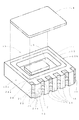
図1に示すように、本発明の一実施の形態に係る電子部品収納用セラミックパッケージ10は、アルミナ(Al2O3)や、窒化アルミニウム(AlN)等のセラミックからなるセラミック基体11に、半導体素子や、発光素子や、水晶振動子等の電子部品12を搭載して収納するものである。この電子部品収納用セラミックパッケージ10は、セラミック基体11が複数枚の板状のセラミック板で積層されてなる四角形状からなり、通常、一方の主面側に電子部品12を収納できるキャビティ部13が設けられている。そして、この電子部品収納用セラミックパッケージ10は、セラミック基体11のキャビティ部13に電子部品12が搭載され、電子部品12と外部とが電気的に導通状態となるようにした後、セラミック基体11に金属板や、セラミック板等からなる蓋体14を接合させることで、キャビティ部13内の電子部品12を気密に封止するようになっている。なお、図示しないが、電子部品収納用セラミックパッケージ10には、電子部品12と外部とを電気的に導通状態とするために、セラミック基体11のキャビティ部13内や、積層された内層にタングステン(W)や、モリブデン(Mo)等の高融点金属を用いた導体配線パターンや、ワイヤボンドパッド等が設けられている。
Next, with reference to the accompanying drawings, embodiments for embodying the present invention will be described for understanding of the present invention.
As shown in FIG. 1, an electronic component housing ceramic package 10 according to an embodiment of the present invention includes a
図2(A)、(B)に示すように、上記の電子部品収納用セラミックパッケージ10は、セラミック基体11の四角形状の一側面15を実装用配線基板16に当接させて垂直に立設させることができるようになっている。これと共に、電子部品収納用セラミックパッケージ10は、セラミック基体11の一側面15、及びこの一側面15近傍のセラミック基体11の両主面の長さ方向に設ける外部接続端子パッド17を実装用配線基板16の半田付け用パッド18に半田19を介して接合させて半田19に良好なメニスカス形状を形成させて搭載できるようになっている。
As shown in FIGS. 2A and 2B, the above-described ceramic package 10 for storing electronic components is vertically erected by bringing one
この電子部品収納用セラミックパッケージ10は、外部接続端子パッド17がセラミック基体11の一側面15、及びこの一側面15近傍のセラミック基体11の両主面の長さ方向両端部のそれぞれに設ける端部端子パッド20を有している。また、この電子部品収納用セラミックパッケージ10は、外部接続端子パッド17が上記の端部端子パッド20と共に、セラミック基体11の一側面15、及びこの一側面15近傍のセラミック基体11の両主面の長さ方向中間部に設ける中間部端子パッド21を有している。この電子部品収納用セラミックパッケージ10は、電子部品12をキャビティ部13に搭載した後、セラミック基体11の一側面15を実装用配線基板16に当接させ立設させて実装できる。また、この電子部品収納用セラミックパッケージ10は、セラミック基体11の一側面15、及びこの一側面15近傍のセラミック基体11の両主面の長さ方向の両端部に設ける端部端子パッド20と、中間部に設ける中間部端子パッド21によって実装用配線基板16との間にできる半田19の良好なメニスカス形状によって強固に接合できる。
In the electronic component storing ceramic package 10, the external
上記の電子部品収納用セラミックパッケージ10は、端部端子パッド20がセラミック基体11の一側面15、及びこの一側面15と直角に隣接するそれぞれ他の側面15a、15bのセラミック基体11の厚みを連通する第1の切り欠き部22を有しているのがよい。そして、端部端子パッド20は、第1の切り欠き部22の表面にセラミック基体11の厚みを連通する、又はセラミック基体11の厚みの中間部で断線する第1のメタライズ膜23を有しているのがよい。更に、端部端子パッド20は、セラミック基体11の両主面の第1の切り欠き部22の近傍に第1のメタライズ膜23と接続して電気的に導通状態からなる第2のメタライズ膜24を有しているのがよい。なお、上記の電子部品収納用セラミックパッケージ10は、端部端子パッド20がセラミック基体11の一側面15と直角に隣接するそれぞれの他の側面15a、15bの第1の切り欠き部22の近傍に第1と、第2のメタライズ膜23、24と電気的に導通状態からなる第3のメタライズ膜(図示せず)を有するものであってもよい。
In the electronic component housing ceramic package 10 described above, the
また、上記の電子部品収納用セラミックパッケージ10は、中間部端子パッド21がセラミック基体11の一側面15のセラミック基体11の厚みを連通する第2の切り欠き部25を有しているのがよい。そして、中間部端子パッド21は、第2の切り欠き部25の表面にセラミック基体11の厚みを連通する、又はセラミック基体11の厚みの中間部で断線する第1のメタライズ膜23aを有しているのがよい。更に、中間部端子パッド21は、セラミック基体11の両主面の第2の切り欠き部25の近傍に第1のメタライズ膜23aと接続して電気的に導通状態からなる第2のメタライズ膜24aを有しているのがよい。
In the electronic component housing ceramic package 10, the
上記の電子部品収納用セラミックパッケージ10は、端部端子パッド20がセラミック基体11の厚みの中間部で断線する第1のメタライズ膜23と、中間部端子パッド21がセラミック基体11の厚みの中間部で断線する第1のメタライズ膜23aを有するようにすることで、セラミック基体11の一側面15側に多数の外部接続端子パッド17が形成できるようになっている。なお、上記の電子部品収納用セラミックパッケージ10は、図示されていないが、通常、第1のメタライズ膜23、23a、及び第2のメタライズ膜24、24aの上面にNiや、Ni合金からなるNiめっき被膜、更にこの上面にAuめっき被膜が形成されている。
In the electronic package housing ceramic package 10 described above, the
ここで、上記の電子部品収納用セラミックパッケージ10の製造方法を簡単に説明する。
上記のような電子部品収納用セラミックパッケージ10には、複数枚のセラミックグリーンシートが用いられている。このセラミックグリーンシートの作製には、例えば、セラミックがアルミナからなる場合に、アルミナ粉末にマグネシア、シリカ、カルシア等の焼結助剤を適当量加えた粉末が準備されている。この粉末には、ジオクチルフタレート等の可塑剤と、アクリル樹脂等のバインダー、及び、トルエン、キシレン、アルコール類等の溶剤を加え、十分に混練した後、脱泡して粘度2000〜40000cpsのスラリーとしている。そして、スラリーは、ドクターブレード法等によって、例えば、厚さ0.25mmのシート状に形成し、更に、適当な大きさにカットした複数枚のセラミックグリーンシートに作製している。このセラミックグリーンシートは、個片体のセラミック基体11がマトリックス状に多数個配列する集合体として形成できる大きさとなっている。
Here, a method for manufacturing the above-described ceramic package 10 for storing electronic components will be briefly described.
A plurality of ceramic green sheets are used in the ceramic package 10 for storing electronic components as described above. For the production of this ceramic green sheet, for example, when the ceramic is made of alumina, a powder is prepared by adding an appropriate amount of a sintering aid such as magnesia, silica, calcia to alumina powder. To this powder, a plasticizer such as dioctyl phthalate, a binder such as acrylic resin, and a solvent such as toluene, xylene, and alcohols are added and kneaded sufficiently, and then defoamed to obtain a slurry having a viscosity of 2000 to 40000 cps. Yes. Then, the slurry is formed into a plurality of ceramic green sheets formed into a sheet having a thickness of, for example, 0.25 mm by a doctor blade method or the like and further cut into an appropriate size. This ceramic green sheet has a size that can be formed as an aggregate in which a large number of individual
次に、複数枚のそれぞれのセラミックグリーンシートには、必要に応じて、複数個の個片体のセラミック基体11用に上下層の電気的導通を形成するためのビア導体用貫通孔や、電子部品を搭載するためのキャビティ部13用の貫通孔や、第1、第2の切り欠き部22、25用の貫通孔を打抜き金型や、パンチングマシーン等を用いて穿設して形成している。更に、それぞれのセラミックグリーンシートには、タングステン(W)や、モリブデン(Mo)等の高融点金属からなる導体ペーストを用いてスクリーン印刷してビア導体用の貫通孔を充填したり、表面に導体配線引廻し用や、第2のメタライズ膜24、24a用等の導体印刷パターンを印刷したり、第1、第2の切り欠き部22、25用の貫通孔の壁面に第1のメタライズ膜23、23a用のスルーホール印刷をしたりしている。
Next, in each of the plurality of ceramic green sheets, via conductor through-holes for forming upper and lower layers of electrical continuity for the plurality of individual
次に、複数枚のこれらのセラミックグリーンシートは、重ね合わされて温度と圧力をかけて積層され、積層体を形成している。そして、積層体には、四角形状のセラミック基体11となる位置のそれぞれにプレス機等に取り付けた切り刃で押圧して積層体の表面に分割溝を形成している。焼成後の電子部品収納用セラミックパッケージ10は、セラミック基体11の一側面15を実装用配線基板16に当接させて立設させることから、例えば、大きさが6×7mm、厚さが2.5mm程度とセラミック基体11としての厚みが比較的厚くなっている。従って、このような厚さの厚い積層体に形成する分割溝は、焼成後の分割時に分割溝の先端同士を結ぶように分割でき、分割後の断面を互いに略同じ程度に2分割させるようにするために、積層体の両主面に形成するのが好ましい。また、一側面15の位置に設ける分割溝は、第1、第2の切り欠き部22、25用の貫通孔の中心を通るようにして設けている。なお、電子部品収納用セラミックパッケージ10には、積層体の段階でセラミック基体11の一側面15となる部分に分割溝を設けないで、焼成後にダイシングソー等の切断機等で第1、第2の切り欠き部22、25用の貫通孔の中心を通るようにして切断することで第1、第2の切り欠き部22、25を有する平坦な一側面15を形成するというような場合もある。
Next, a plurality of these ceramic green sheets are overlaid and laminated by applying temperature and pressure to form a laminated body. Then, the laminated body is pressed with a cutting blade attached to a press or the like at each of the positions where the quadrangular
次に、積層体は、還元雰囲気中の1550℃程度の温度でセラミックグリーンシートと、高融点金属を同時焼成して焼成体を形成している。この焼成体は、焼成によってセラミックグリーンシートの積層体から約30%程度収縮したセラミック基体11の集合体とし、セラミックグリーンシートの表面や、第1、第2の切り欠き部22、25用の貫通孔の壁面に形成されている導体印刷パターン等をそれぞれのセラミック基体11に焼き付けた第1、第2のメタライズ膜23、23a、24、24a等としている。そして、この焼成体は、外部に露出する金属部分にNiめっき被膜及びAuめっき被膜を形成した後、分割溝で分割したり、セラミック基体11の所望の一側面となる位置を切断したりして個片の電子部品収納用セラミックパッケージ10を形成している。
Next, the laminate is formed by simultaneously firing the ceramic green sheet and the refractory metal at a temperature of about 1550 ° C. in a reducing atmosphere. This fired body is an aggregate of the
本発明の電子部品収納用セラミックパッケージは、半導体素子や、発光素子や、水晶振動子等の電子部品を搭載した後、ボード等の実装用配線基板にセラミック基体の一側面を当接させパッケージを立設させて実装でき、実装密度を向上させる必要のある様々な電子装置に組み込んで用いることができる。 The ceramic package for electronic component storage according to the present invention includes a semiconductor element, a light emitting element, a crystal resonator, and other electronic components mounted thereon, and then a side surface of the ceramic substrate is brought into contact with a mounting wiring board such as a board. It can be mounted upright and can be used by being incorporated in various electronic devices that need to improve the mounting density.
10:電子部品収納用セラミックパッケージ、11:セラミック基体、12:電子部品、13:キャビティ部、14:蓋体、15:一側面、15a、15b:他の側面、16:実装用配線記板、17:外部接続端子パッド、18:半田付け用パッド、19:半田、20:端部端子パッド、21:中間部端子パッド、22:第1の切り欠き部、23、23a:第1のメタライズ膜、24、24a:第2のメタライズ膜、25:第2の切り欠き部
10: Ceramic package for storing electronic components, 11: Ceramic substrate, 12: Electronic components, 13: Cavity, 14: Lid, 15: One side, 15a, 15b: Other side, 16: Wiring board for mounting, 17: external connection terminal pad, 18: soldering pad, 19: solder, 20: end terminal pad, 21: intermediate terminal pad, 22: first notch, 23, 23a: first metallized
Claims (2)
前記外部接続端子パッドが前記セラミック基体の前記一側面、及び該一側面近傍の前記セラミック基体の両主面の長さ方向両端部のそれぞれに設ける端部端子パッドと、前記一側面、及び該一側面近傍の前記セラミック基体の両主面の長さ方向中間部に設ける中間部端子パッドを有することを特徴とする電子部品収納用セラミックパッケージ。 One side surface of a ceramic substrate having a quadrangular shape capable of storing electronic components is brought into contact with the mounting wiring board so as to stand vertically, and in order to electrically connect the electronic components with the outside, In the ceramic package for storing electronic components that can be mounted by bonding the external connection terminal pads to be provided to the soldering pads of the mounting wiring board via solder,
The external connection terminal pads are provided on the one side surface of the ceramic base and on both end portions in the length direction of both main surfaces of the ceramic base in the vicinity of the one side surface, the one side surface, and the one side surface. A ceramic package for storing electronic components, comprising intermediate terminal pads provided at intermediate portions in the longitudinal direction of both main surfaces of the ceramic base in the vicinity of the side surface.
Priority Applications (1)
| Application Number | Priority Date | Filing Date | Title |
|---|---|---|---|
| JP2009266513A JP2011114031A (en) | 2009-11-24 | 2009-11-24 | Ceramic package for storing electronic component |
Applications Claiming Priority (1)
| Application Number | Priority Date | Filing Date | Title |
|---|---|---|---|
| JP2009266513A JP2011114031A (en) | 2009-11-24 | 2009-11-24 | Ceramic package for storing electronic component |
Publications (1)
| Publication Number | Publication Date |
|---|---|
| JP2011114031A true JP2011114031A (en) | 2011-06-09 |
Family
ID=44236160
Family Applications (1)
| Application Number | Title | Priority Date | Filing Date |
|---|---|---|---|
| JP2009266513A Pending JP2011114031A (en) | 2009-11-24 | 2009-11-24 | Ceramic package for storing electronic component |
Country Status (1)
| Country | Link |
|---|---|
| JP (1) | JP2011114031A (en) |
Cited By (2)
| Publication number | Priority date | Publication date | Assignee | Title |
|---|---|---|---|---|
| JP2014067922A (en) * | 2012-09-26 | 2014-04-17 | Nippon Steel & Sumikin Electronics Devices Inc | Ceramic component and manufacturing method therefor |
| CN107768323A (en) * | 2017-11-24 | 2018-03-06 | 安徽北方芯动联科微系统技术有限公司 | Anti high overload electron device package shell |
Citations (6)
| Publication number | Priority date | Publication date | Assignee | Title |
|---|---|---|---|---|
| JPH0685163A (en) * | 1992-09-03 | 1994-03-25 | Fujitsu Ltd | Vertically mounted semiconductor device |
| JPH0837251A (en) * | 1994-07-21 | 1996-02-06 | Murata Mfg Co Ltd | Laminated electronic part and manufacture thereof |
| JP2000196000A (en) * | 1998-12-25 | 2000-07-14 | Rohm Co Ltd | Chip electronic component and method of manufacturing the same |
| JP2004281994A (en) * | 2003-01-24 | 2004-10-07 | Kyocera Corp | Light emitting element storage package and light emitting device |
| JP2007132687A (en) * | 2005-11-08 | 2007-05-31 | Sensata Technologies Japan Ltd | Package for sensor, and detector using the same |
| JP2007227739A (en) * | 2006-02-24 | 2007-09-06 | Kyocera Corp | Electronic component storage package and electronic component device |
-
2009
- 2009-11-24 JP JP2009266513A patent/JP2011114031A/en active Pending
Patent Citations (6)
| Publication number | Priority date | Publication date | Assignee | Title |
|---|---|---|---|---|
| JPH0685163A (en) * | 1992-09-03 | 1994-03-25 | Fujitsu Ltd | Vertically mounted semiconductor device |
| JPH0837251A (en) * | 1994-07-21 | 1996-02-06 | Murata Mfg Co Ltd | Laminated electronic part and manufacture thereof |
| JP2000196000A (en) * | 1998-12-25 | 2000-07-14 | Rohm Co Ltd | Chip electronic component and method of manufacturing the same |
| JP2004281994A (en) * | 2003-01-24 | 2004-10-07 | Kyocera Corp | Light emitting element storage package and light emitting device |
| JP2007132687A (en) * | 2005-11-08 | 2007-05-31 | Sensata Technologies Japan Ltd | Package for sensor, and detector using the same |
| JP2007227739A (en) * | 2006-02-24 | 2007-09-06 | Kyocera Corp | Electronic component storage package and electronic component device |
Cited By (3)
| Publication number | Priority date | Publication date | Assignee | Title |
|---|---|---|---|---|
| JP2014067922A (en) * | 2012-09-26 | 2014-04-17 | Nippon Steel & Sumikin Electronics Devices Inc | Ceramic component and manufacturing method therefor |
| CN107768323A (en) * | 2017-11-24 | 2018-03-06 | 安徽北方芯动联科微系统技术有限公司 | Anti high overload electron device package shell |
| CN107768323B (en) * | 2017-11-24 | 2023-12-05 | 安徽芯动联科微系统股份有限公司 | High overload resistant electronic device packaging shell |
Similar Documents
| Publication | Publication Date | Title |
|---|---|---|
| JP2009158511A (en) | Input/output terminal and package for housing semiconductor device | |
| JP2011114031A (en) | Ceramic package for storing electronic component | |
| JP2011114032A (en) | Ceramic package for storing electronic component | |
| JP6108734B2 (en) | Electronic component element storage package | |
| JP6698301B2 (en) | Wiring board, electronic device and electronic module | |
| JP4006686B2 (en) | Ceramic multilayer substrate and manufacturing method thereof | |
| JP7145739B2 (en) | Wiring boards, electronic devices and electronic modules | |
| JP2007048798A (en) | Ceramic package for housing electronic component | |
| JP6595580B2 (en) | Wiring board, electronic device and electronic module | |
| JP2006173287A (en) | Ceramic package for storing electronic components and manufacturing method thereof | |
| JP6737646B2 (en) | Wiring board, electronic device and electronic module | |
| JP2007242908A (en) | Ceramic package for electronic component storage | |
| JP4345971B2 (en) | Manufacturing method of ceramic package | |
| JP5254946B2 (en) | Package for storing semiconductor elements | |
| JP2005111856A (en) | Chucking plate for screen printing | |
| JP4167614B2 (en) | Electronic component storage package | |
| JP2011223425A (en) | Package for housing electronic component elements | |
| JP2006279536A (en) | Manufacturing method of ceramic package for housing piezoelectric device | |
| JP2004288661A (en) | Wiring board | |
| JP4986500B2 (en) | Laminated substrate, electronic device and manufacturing method thereof. | |
| JP4377729B2 (en) | Wiring board | |
| JP2005268350A (en) | Package for storing electronic component | |
| JP2003068920A (en) | Wiring board | |
| JP6231376B2 (en) | Semiconductor element mounting substrate and semiconductor device | |
| JP2005158821A (en) | Package for housing semiconductor element and manufacturing method thereof |
Legal Events
| Date | Code | Title | Description |
|---|---|---|---|
| A621 | Written request for application examination |
Free format text: JAPANESE INTERMEDIATE CODE: A621 Effective date: 20121115 |
|
| A131 | Notification of reasons for refusal |
Free format text: JAPANESE INTERMEDIATE CODE: A131 Effective date: 20130626 |
|
| A977 | Report on retrieval |
Free format text: JAPANESE INTERMEDIATE CODE: A971007 Effective date: 20130627 |
|
| A521 | Written amendment |
Free format text: JAPANESE INTERMEDIATE CODE: A523 Effective date: 20130820 |
|
| A131 | Notification of reasons for refusal |
Free format text: JAPANESE INTERMEDIATE CODE: A131 Effective date: 20140507 |
|
| A521 | Written amendment |
Free format text: JAPANESE INTERMEDIATE CODE: A523 Effective date: 20140616 |
|
| A02 | Decision of refusal |
Free format text: JAPANESE INTERMEDIATE CODE: A02 Effective date: 20150202 |