JP2011129934A - Variable resistance memory device and method of manufacturing the same - Google Patents
Variable resistance memory device and method of manufacturing the same Download PDFInfo
- Publication number
- JP2011129934A JP2011129934A JP2010284395A JP2010284395A JP2011129934A JP 2011129934 A JP2011129934 A JP 2011129934A JP 2010284395 A JP2010284395 A JP 2010284395A JP 2010284395 A JP2010284395 A JP 2010284395A JP 2011129934 A JP2011129934 A JP 2011129934A
- Authority
- JP
- Japan
- Prior art keywords
- variable resistance
- memory device
- pattern
- line
- interlayer insulating
- Prior art date
- Legal status (The legal status is an assumption and is not a legal conclusion. Google has not performed a legal analysis and makes no representation as to the accuracy of the status listed.)
- Granted
Links
Images


Classifications
-
- H—ELECTRICITY
- H10—SEMICONDUCTOR DEVICES; ELECTRIC SOLID-STATE DEVICES NOT OTHERWISE PROVIDED FOR
- H10N—ELECTRIC SOLID-STATE DEVICES NOT OTHERWISE PROVIDED FOR
- H10N70/00—Solid-state devices having no potential barriers, and specially adapted for rectifying, amplifying, oscillating or switching
- H10N70/011—Manufacture or treatment of multistable switching devices
-
- H—ELECTRICITY
- H10—SEMICONDUCTOR DEVICES; ELECTRIC SOLID-STATE DEVICES NOT OTHERWISE PROVIDED FOR
- H10N—ELECTRIC SOLID-STATE DEVICES NOT OTHERWISE PROVIDED FOR
- H10N70/00—Solid-state devices having no potential barriers, and specially adapted for rectifying, amplifying, oscillating or switching
- H10N70/20—Multistable switching devices, e.g. memristors
- H10N70/231—Multistable switching devices, e.g. memristors based on solid-state phase change, e.g. between amorphous and crystalline phases, Ovshinsky effect
-
- G—PHYSICS
- G11—INFORMATION STORAGE
- G11C—STATIC STORES
- G11C13/00—Digital stores characterised by the use of storage elements not covered by groups G11C11/00, G11C23/00, or G11C25/00
- G11C13/0002—Digital stores characterised by the use of storage elements not covered by groups G11C11/00, G11C23/00, or G11C25/00 using resistive RAM [RRAM] elements
- G11C13/0004—Digital stores characterised by the use of storage elements not covered by groups G11C11/00, G11C23/00, or G11C25/00 using resistive RAM [RRAM] elements comprising amorphous/crystalline phase transition cells
-
- H—ELECTRICITY
- H10—SEMICONDUCTOR DEVICES; ELECTRIC SOLID-STATE DEVICES NOT OTHERWISE PROVIDED FOR
- H10B—ELECTRONIC MEMORY DEVICES
- H10B63/00—Resistance change memory devices, e.g. resistive RAM [ReRAM] devices
- H10B63/80—Arrangements comprising multiple bistable or multi-stable switching components of the same type on a plane parallel to the substrate, e.g. cross-point arrays
-
- H—ELECTRICITY
- H10—SEMICONDUCTOR DEVICES; ELECTRIC SOLID-STATE DEVICES NOT OTHERWISE PROVIDED FOR
- H10N—ELECTRIC SOLID-STATE DEVICES NOT OTHERWISE PROVIDED FOR
- H10N70/00—Solid-state devices having no potential barriers, and specially adapted for rectifying, amplifying, oscillating or switching
- H10N70/011—Manufacture or treatment of multistable switching devices
- H10N70/061—Shaping switching materials
- H10N70/066—Shaping switching materials by filling of openings, e.g. damascene method
-
- H—ELECTRICITY
- H10—SEMICONDUCTOR DEVICES; ELECTRIC SOLID-STATE DEVICES NOT OTHERWISE PROVIDED FOR
- H10N—ELECTRIC SOLID-STATE DEVICES NOT OTHERWISE PROVIDED FOR
- H10N70/00—Solid-state devices having no potential barriers, and specially adapted for rectifying, amplifying, oscillating or switching
- H10N70/801—Constructional details of multistable switching devices
- H10N70/821—Device geometry
- H10N70/826—Device geometry adapted for essentially vertical current flow, e.g. sandwich or pillar type devices
- H10N70/8265—Device geometry adapted for essentially vertical current flow, e.g. sandwich or pillar type devices on sidewalls of dielectric structures, e.g. mesa-shaped or cup-shaped devices
-
- H—ELECTRICITY
- H10—SEMICONDUCTOR DEVICES; ELECTRIC SOLID-STATE DEVICES NOT OTHERWISE PROVIDED FOR
- H10N—ELECTRIC SOLID-STATE DEVICES NOT OTHERWISE PROVIDED FOR
- H10N70/00—Solid-state devices having no potential barriers, and specially adapted for rectifying, amplifying, oscillating or switching
- H10N70/801—Constructional details of multistable switching devices
- H10N70/861—Thermal details
- H10N70/8616—Thermal insulation means
-
- H—ELECTRICITY
- H10—SEMICONDUCTOR DEVICES; ELECTRIC SOLID-STATE DEVICES NOT OTHERWISE PROVIDED FOR
- H10N—ELECTRIC SOLID-STATE DEVICES NOT OTHERWISE PROVIDED FOR
- H10N70/00—Solid-state devices having no potential barriers, and specially adapted for rectifying, amplifying, oscillating or switching
- H10N70/801—Constructional details of multistable switching devices
- H10N70/881—Switching materials
- H10N70/882—Compounds of sulfur, selenium or tellurium, e.g. chalcogenides
Landscapes
- Engineering & Computer Science (AREA)
- Manufacturing & Machinery (AREA)
- Chemical & Material Sciences (AREA)
- Crystallography & Structural Chemistry (AREA)
- Semiconductor Memories (AREA)
Abstract
【課題】可変抵抗メモリ装置及びその製造方法を提供する。
【解決手段】可変抵抗メモリ装置及びその製造方法を提供する。基板上に複数の下部電極を構成し、前記下部電極を露出し、第1方向に延長されるトレンチを含む第1層間絶縁膜を構成し、前記第1層間絶縁膜上に前記第1方向と交差する第2方向に延長される上部電極を構成し、前記トレンチ内に前記上部電極の側壁にアライメントされる側壁を有する可変抵抗パターンを形成する。
【選択図】図2A variable resistance memory device and a method of manufacturing the same are provided.
A variable resistance memory device and a method of manufacturing the same are provided. Forming a plurality of lower electrodes on the substrate; exposing the lower electrodes; forming a first interlayer insulating film including a trench extending in a first direction; and forming the first direction on the first interlayer insulating film; An upper electrode extending in the intersecting second direction is formed, and a variable resistance pattern having a sidewall aligned with the sidewall of the upper electrode is formed in the trench.
[Selection] Figure 2
Description
本発明は半導体装置に関し、さらに詳しくは、可変抵抗メモリ装置及びその製造方法に関する。 The present invention relates to a semiconductor device, and more particularly to a variable resistance memory device and a manufacturing method thereof.
一般に、半導体メモリ装置は揮発性(volatile)メモリ装置と不揮発性(nonvolatile)メモリ装置に分けられる。 Generally, the semiconductor memory device is divided into a volatile memory device and a non-volatile memory device.
揮発性メモリ装置は電源の供給が遮断されると、貯蔵されたデータが消去されるメモリ装置、例えば、DRAM(Dynamic Random Access Memory)及びSRAM(Static Random Access Memory)等がある。そして、不揮発性メモリ装置は電源の供給が遮断されても貯蔵されたデータが消去されないメモリ装置、例えば、PROM(Programmable ROM)、EPROM(Erasable PROM)、EEPROM(Electrically EPROM)、フラッシュメモリ装置(Flash Memory Device)等がある。 The volatile memory device includes a memory device in which stored data is erased when power supply is cut off, for example, a DRAM (Dynamic Random Access Memory) and a SRAM (Static Random Access Memory). The nonvolatile memory device is a memory device in which stored data is not erased even when power supply is cut off, for example, PROM (Programmable ROM), EPROM (Erasable PROM), EEPROM (Electrically EPROM), flash memory device (Flash Memory Device).
最近、半導体メモリ装置の高性能化及び低電力化により、FRAM(Ferroelectric Random Access Memory)、MRAM(Magnetic Random Access Memory)及びPRAM(Phase−Change Random Access Memory)のような次世代の半導体メモリ装置等が開発されている。斯かる次世代の半導体メモリ装置を構成する物質等は電流又は電圧によって、抵抗値が異なり、電流又は電圧の供給が遮断されても抵抗値をそのまま維持する特性を有する。 Recently, due to high performance and low power consumption of semiconductor memory devices, next-generation memory devices such as FRAM (Ferroelectric Random Access Memory), MRAM (Magnetic Random Access Memory) and PRAM (Phase-Change Random Access Memory). Has been developed. Substances and the like constituting such a next-generation semiconductor memory device have different resistance values depending on current or voltage, and have a characteristic of maintaining the resistance value as it is even when supply of current or voltage is cut off.
本発明が解決しようとする課題は、電気特性及び信頼性が向上される可変抵抗メモリ装置及びその製造方法を提供することである。
また、本発明が解決しようとする他の課題等は、次の説明から明らかになるであろう。
The problem to be solved by the present invention is to provide a variable resistance memory device with improved electrical characteristics and reliability and a method of manufacturing the same.
Further, other problems to be solved by the present invention will become clear from the following description.
本発明の課題等を解決するための可変抵抗メモリ装置を提供する。該可変抵抗メモリ装置は基板、前記基板上の複数の下部電極、前記下部電極を露出し、第1方向に延長されるトレンチを含む第1層間絶縁膜、前記第1層間絶縁膜上に形成され、前記第1方向と交差する第2方向に延長される上部電極、前記トレンチ内に形成され、前記上部電極の側壁にアライメントされる側壁を含む複数の可変抵抗パターンを有する。本発明の一実施形態において、前記トレンチは前記第2方向に隣接する2つの下部電極をともに露出する。 A variable resistance memory device for solving the problems of the present invention is provided. The variable resistance memory device is formed on a substrate, a plurality of lower electrodes on the substrate, a first interlayer insulating film including a trench that exposes the lower electrode and extends in a first direction, and the first interlayer insulating film. And an upper electrode extending in a second direction intersecting the first direction, and a plurality of variable resistance patterns including a sidewall formed in the trench and aligned with the sidewall of the upper electrode. In one embodiment of the present invention, the trench exposes two lower electrodes adjacent in the second direction.
本発明の異なる実施形態において、前記可変抵抗パターンは前記第1方向に各下部電極上に分離されて形成される島型である。 In another embodiment of the present invention, the variable resistance pattern is an island type formed separately on each lower electrode in the first direction.
本発明のまた異なる実施形態において、前記可変抵抗メモリ装置は基板、前記基板上の複数の下部電極、前記下部電極上に形成され、第1方向に延長される可変抵抗ライン、前記可変抵抗ライン上に形成され、前記第1方向と交差する第2方向に延長される上部電極を含む。 In another embodiment of the present invention, the variable resistance memory device includes a substrate, a plurality of lower electrodes on the substrate, a variable resistance line formed on the lower electrode and extending in a first direction, and on the variable resistance line. And an upper electrode extending in a second direction intersecting the first direction.
また、上述した課題等を解決するための可変抵抗メモリ装置の製造方法を提供する。該製造方法は基板上に複数の下部電極を形成し、前記下部電極上に第1方向に延長される可変抵抗ラインを形成し、前記可変抵抗ライン上に、前記第1方向と交差する第2方向に延長される上部電極を形成することを含む。 In addition, a method of manufacturing a variable resistance memory device for solving the above-described problems and the like is provided. The manufacturing method includes forming a plurality of lower electrodes on a substrate, forming a variable resistance line extending in a first direction on the lower electrode, and a second crossing the first direction on the variable resistance line. Forming a top electrode extending in the direction.
本発明の一実施形態において、前記上部電極を形成することは、前記可変抵抗ライン上に導電膜を形成し、前記導電膜上に前記第2方向に延長されるマスクパターンを形成し、前記マスクパターンによって前記導電膜を前記第2方向に延長されるようにパターニングすることを含む。 In one embodiment of the present invention, forming the upper electrode includes forming a conductive film on the variable resistance line, forming a mask pattern extending in the second direction on the conductive film, and forming the mask Patterning the conductive film to extend in the second direction according to a pattern.
本発明の異なる実施形態において、前記マスクパターンによってパターニングすることは、前記可変抵抗ラインをパターニングして前記第1方向に分離された可変抵抗パターンを形成することを含む。 In another embodiment of the present invention, patterning with the mask pattern includes patterning the variable resistance line to form a variable resistance pattern separated in the first direction.
本発明のまた異なる実施形態において、前記可変抵抗ラインを形成することは、前記下部電極上に層間絶縁膜を形成し、前記層間絶縁膜に前記第1方向に延長され、前記下部電極の上面の少なくとも一部を露出するトレンチを形成し、前記トレンチ上に可変抵抗物質膜を形成することを含む。 In another embodiment of the present invention, forming the variable resistance line includes forming an interlayer insulating film on the lower electrode, extending in the first direction to the interlayer insulating film, and forming an upper surface of the lower electrode. Forming a trench exposing at least a part thereof, and forming a variable resistance material film on the trench.
上部電極と可変抵抗パターンの誤整列の問題を解決できる。従って、電気特性及び信頼性が向上される可変抵抗メモリ装置を提供することができる。 The problem of misalignment between the upper electrode and the variable resistance pattern can be solved. Therefore, a variable resistance memory device with improved electrical characteristics and reliability can be provided.
本発明の長所及び特徴、そして、本発明の課題を解決するための方法は添付の図面と後述の実施形態によって明確になるであろう。 Advantages and features of the present invention and methods for solving the problems of the present invention will be apparent from the accompanying drawings and embodiments described below.
しかし、本発明は以下に開示される実施形態によって限定されず、異なる様々な形態で具現できる。ここに紹介する実施形態は開示される内容が完全になるように、そして、当業者等に本発明の思想が十分に伝えられるように提供されるものである。 However, the present invention is not limited to the embodiments disclosed below, and can be embodied in various different forms. The embodiments introduced herein are provided so that the disclosed contents are complete, and the concept of the present invention is sufficiently communicated to those skilled in the art.
また、本発明の明細書から、導電性膜、半導体膜又は絶縁性膜等のある物質膜が異なる物質膜又は基板“上”にあるものと言及された場合、斯かる物質膜は異なる物質膜又は基板上に直接形成されたり、それらの間に他の物質膜が介されたりすることも含む。 In addition, when the specification of the present invention mentions that a certain material film such as a conductive film, a semiconductor film, or an insulating film is on a different material film or substrate “on”, such a material film is a different material film. Alternatively, it may be formed directly on the substrate, or another material film may be interposed between them.
また、本明細書の様々な実施形態等から第1、第2、第3等の用語が物質膜又は工程段階を説明するために使われるが、斯かる用語等は、但し、ある特定の物質膜又は工程段階を異なる物質膜又は異なる工程段階と区別するために使われるだけである。 In addition, terms such as the first, second, and third terms are used to describe a material film or a process step from various embodiments of the present specification, but such terms and the like may be used only for a specific substance. It is only used to distinguish films or process steps from different material films or different process steps.
本発明の明細書から言及される用語は実施形態等を説明するためのものであり、本発明を制限するものではない。本発明の明細書から、単数形は特別に言及されていない限り複数形も含む。明細書から言及される‘含む’(comprises、comprising)は1つ以上の異なる構成要素の存在又は追加を排除しない。 The terms mentioned in the specification of the present invention are for describing the embodiments and the like, and are not intended to limit the present invention. From the specification of the present invention, the singular includes the plural unless specifically stated otherwise. “Contains” (comprising) as referred to from the specification does not exclude the presence or addition of one or more different components.
また、本発明の明細書から記述される実施形態等は、本発明の理想的な例示図、即ち、断面図及び/又は平面図等を参照して説明する。図面において、膜及び領域等の厚さは技術の効果的な説明のために誇張された。従って、製造技術及び/又は誤差等によって例示図の形態を変形できる。 In addition, embodiments and the like described from the specification of the present invention will be described with reference to ideal exemplary views of the present invention, that is, cross-sectional views and / or plan views. In the drawings, the thickness of films and regions are exaggerated for effective description of the technology. Therefore, the form of the exemplary drawing can be modified by manufacturing technique and / or error.
従って、本発明の実施形態等は示された特定の形態に限らず、製造工程によって生成される形態の変化も含む。例えば、直角で示されたエッチング領域はラウンドされたり、所定の曲率を有する形態も含む。従って、図面から例示された領域等の形態は素子の領域の特定形態を例示するためであり、発明の範囲を限定するものではない。 Accordingly, the embodiments of the present invention are not limited to the specific forms shown, but also include changes in the forms generated by the manufacturing process. For example, the etching region indicated by a right angle includes a form that is rounded or has a predetermined curvature. Therefore, the form of the region and the like illustrated from the drawings is for illustrating the specific form of the region of the element, and does not limit the scope of the invention.
以下に、図面等を参照して、本発明の実施形態等による可変抵抗メモリ装置及びその製造方法に対して詳しく説明する。 Hereinafter, a variable resistance memory device according to an embodiment of the present invention and a method for manufacturing the same will be described in detail with reference to the drawings.
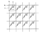
図1は、本発明の実施形態等による可変抵抗メモリ装置のメモリセルアレイを示す回路図である。 FIG. 1 is a circuit diagram showing a memory cell array of a variable resistance memory device according to an embodiment of the present invention.
図1を参照すると、複数のメモリセル10がマトリックスの形態で配列される。前記メモリセル10は可変抵抗素子11と選択素子12を含む。前記可変抵抗素子11と前記選択素子12はビットラインBLとワードラインWLとの間に介される。
Referring to FIG. 1, a plurality of
前記可変抵抗素子11は前記ビットラインBLを通じて供給される電流の量によって状態が決まる。前記選択素子12は前記可変抵抗素子11と前記ワードラインWLとの間に接続され、前記ワードラインWLの電圧によって前記可変抵抗素子11への電流の供給を制御する。前記選択素子12はダイオード(diode)、MOSトランジスタ又はバイポーラ(bipolar)トランジスタからなる。
The state of the variable resistance element 11 is determined by the amount of current supplied through the bit line BL. The
本発明の実施形態等において、前記可変抵抗素子11として相変化物質を採択したメモリセル等を含む相変化メモリ装置を一例として説明する。しかし、本発明の技術思想はこれに制限されない。前記相変化物質は温度及び冷却時間によって比較的抵抗が高い非晶質状態と、比較的抵抗が低い結晶質状態を有する。前記非晶質状態はセット(SET)状態であり、前記結晶質状態はリセット(RESET)状態である。斯かる相変化メモリ素子は下部電極を通じて供給される電流によってジュール熱(Joule´s heat)が発生して相変化物質を加熱させる。この際、ジュール熱は相変化物質の比抵抗及び電流の供給時間に比例して発生する。 In an embodiment of the present invention, a phase change memory device including a memory cell that adopts a phase change material as the variable resistance element 11 will be described as an example. However, the technical idea of the present invention is not limited to this. The phase change material has an amorphous state with a relatively high resistance and a crystalline state with a relatively low resistance depending on temperature and cooling time. The amorphous state is a set (SET) state, and the crystalline state is a reset (RESET) state. In such a phase change memory device, Joule's heat is generated by current supplied through the lower electrode to heat the phase change material. At this time, Joule heat is generated in proportion to the specific resistance of the phase change material and the current supply time.
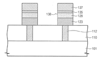
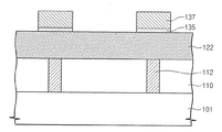
図2は本発明の第1実施形態による可変抵抗メモリ装置の平面図である。図3及び図4は本発明の第1実施形態による可変抵抗メモリ装置の断面図である。図3及び図4は各々図2のA−A’線及びB−B’線に沿って切断した断面図である。 FIG. 2 is a plan view of the variable resistance memory device according to the first embodiment of the present invention. 3 and 4 are cross-sectional views of the variable resistance memory device according to the first embodiment of the present invention. 3 and 4 are cross-sectional views taken along lines A-A 'and B-B' in FIG. 2, respectively.
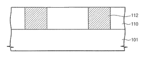
図2、図3及び図4を参照すると、基板101上に下部電極112を含む第1層間絶縁膜110が形成される。前記基板101は第1方向に延長されるワードラインWLを含む。前記ワードラインWLは不純物がドープされたドープラインである。また、前記半導体基板は複数の前記ワードラインWLに電気的に接触された選択素子(図示せず)を含む。前記下部電極112は上面が一字形(line type)、弧形(arc type)、円形、四角形又はリング形(ring type)からなる。本実施形態において、前記下部電極112は前記第1方向と交差する第2方向に一列に配列された一字形(line type)からなる。即ち、前記下部電極112の上面は前記第2方向に長軸を有し、前記第1方向に短軸を有する。
Referring to FIGS. 2, 3, and 4, a first
前記下部電極112上には可変抵抗パターン123、例えば、相変化物質パターンが形成される。前記可変抵抗パターン123は状態が可逆的に変化できる物質で形成される。前記可変抵抗パターン123はカルコゲナイド(chalcogenide)系元素であるTe及びSe中で少なくとも1つと、Ge、Sb、Bi、Pb、Sn、Ag、As、S、Si、P、O及びCの中で選択される少なくとも1つが混合された化合物から構成される。本実施形態において、前記可変抵抗パターン123はU字形からなる。前記可変抵抗パターン123は前記第1方向に延長されるトレンチ115内に形成される。前記トレンチ115は第2層間絶縁膜120に形成される。従って、前記可変抵抗パターン123は前記第2方向に下部電極112上に分離されて形成される。また、前記可変抵抗パターン123は前記第1方向に分離されるよう形成される。即ち、前記可変抵抗パターン123は図3に示したように前記第1方向に下部電極112上に分離されて形成される。即ち、前記可変抵抗パターン123は下部電極112上に島型(isolated type)に形成される。前記可変抵抗パターン123の島型の構造はセル間の干渉現象を緩和させる。
A
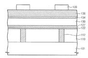
前記可変抵抗パターン123上に熱損失防止パターン128が形成される。前記熱損失防止パターン128は相変化物質が加熱されるとき発生する熱が損失されることを防止する。従って、小さい電流量で相変化物質を溶融点まで加熱することができる。即ち、可変抵抗メモリ装置の消費電力を減らすことができる。前記熱損失防止パターン128は、例えば、SiON、C、ALD−AlN、GeN、Al2O3、MgO、SiO2、CaO、Y2O3、TiO2、Cr2O3、FeO、CoO、ZrO及びCuO2の中で選択される何れか1つを含む絶縁膜で形成される。
A heat
前記熱損失防止パターン128は前記可変抵抗パターン123上に前記可変抵抗パターン123と同様な形状で形成される。前記熱損失防止パターン128上に前記トレンチ115を埋める絶縁パターン131が形成される。前記絶縁パターン131は酸化膜からなる。
The heat
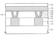
前記可変抵抗パターン123上には、前記第2方向に延長される上部電極137が形成される。前記上部電極137は前記トレンチ115と交差する。前記可変抵抗パターン123と前記上部電極137との間には拡散防止パターン135が形成される。前記拡散防止パターン135は前記第2方向に延長される。
An
前記可変抵抗パターン123、前記熱損失防止パターン128、前記絶縁パターン131、前記拡散防止パターン135及び前記上部電極137は図3に示したようにアライメントされた(aligned)側壁138を有する。即ち、前記可変抵抗パターン123、前記熱損失防止パターン128、前記絶縁パターン131は前記上部電極137の側壁に整列された側壁を含む。前記アライメントされた側壁138の間に第3層間絶縁膜140が形成される。
The
前記上部電極137上に前記ワードラインWLと交差するビットラインBLが形成される。前記ビットラインBLは第4層間絶縁膜145のコンタクトプラグ141を通じて前記上部電極137と電気的に接続される。
A bit line BL intersecting with the word line WL is formed on the
本実施形態において、前記上部電極137とアライメントされた前記可変抵抗パターン123の側壁は前記下部電極112とは相対的に遠い距離を置いて配置される。従って、前記可変抵抗パターン123のパターニングの際、発生する損傷による電気特性の劣化が改善される。
In this embodiment, the sidewall of the
続いて、本発明の第1実施形態による可変抵抗メモリ装置の製造方法を説明する。 Next, a method for manufacturing the variable resistance memory device according to the first embodiment of the present invention will be described.
図5、図7、図9、図11、図13は本発明の第1実施形態による可変抵抗メモリ装置の製造方法を順に示す図2のA−A’線に沿って切断した断面図である。図6、図8、図10、図12、図14は本発明の第1実施形態による可変抵抗メモリ装置の製造方法を順に示す図2のB−B’線に沿って切断した断面図である。 5, FIG. 7, FIG. 9, FIG. 11 and FIG. 13 are cross-sectional views taken along the line AA 'of FIG. 2 sequentially illustrating the method of manufacturing the variable resistance memory device according to the first embodiment of the present invention. . 6, 8, 10, 12, and 14 are cross-sectional views taken along line BB ′ of FIG. 2 sequentially illustrating a method of manufacturing the variable resistance memory device according to the first embodiment of the present invention. .
図2、図5及び図6を参照すると、ワードラインWL及び選択素子(図示せず)を含む基板101が形成される。前記基板101内の前記ワードラインWLはライン形態で不純物がドープされた不純物領域であり、前記ワードラインWL間に素子分離膜(図示せず)を形成する。前記ワードラインWL上にはダイオード又はトランジスタのような選択素子(図示せず)が形成される。先ず、前記基板101上に第1層間絶縁膜110を形成する。前記第1層間絶縁膜110は、例えば、BSG(Borosilicate Glass)、PSG(Phosphosilicate Glass)、BPSG(Borophosphosilicate Glass)、PE−TEOS(Plasma Enhanced Tetra Ethyl Ortho Silicate)又はHDP(High Density Plasma)等のようなシリコーン酸化膜からなる。以下に、説明する異なる層間絶縁膜も同じ物質からなる。前記第1層間絶縁膜110に下部電極112が形成される。前記下部電極112は前記ワードラインWL上から前記第2方向への長さが前記第1方向への長さより長く形成される。前記下部電極112は前記第1層間絶縁膜110をパターニングした後、導電膜を蒸着して形成する。前記導電膜の蒸着後、平坦化工程が行なわれる。前記下部電極112は、例えば、Ti、TiSix、TiN、TiON、TiW、TiAlN、TiAlON、TiSiN、TiBN、W、WSix、WN、WON、WSiN、WBN、WCN、Ta、TaSix、TaN、TaON、TaAlN、TaSiN、TaCN、Mo、MoN、MOSiN、MoAlN、NbN、ZrSiN、ZrAlN、Ru、CoSix、NiSix、導電性炭素(conductive carbon)、Cu及びこれらの組合からなる群から選択される物質で形成される。
Referring to FIGS. 2, 5 and 6, a
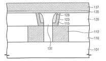
図2、図7及び図8を参照すると、前記下部電極112上に第2層間絶縁膜120が形成される。前記第2層間絶縁膜120がパターニングされて前記第1方向に延長されるトレンチ115が形成される。前記トレンチ115は前記下部電極112の上面の少なくとも一部を露出するよう形成される。前記トレンチ115は上部から下部の方に幅がだんだん減少するよう前記第2層間絶縁膜120を異方性エッチングして形成される。
Referring to FIGS. 2, 7 and 8, a second
前記トレンチ115の側壁及び底面と前記第2層間絶縁膜120上に可変抵抗物質膜121が形成される。前記可変抵抗物質膜121は前記下部電極112と電気的に接続される。前記可変抵抗物質膜121はカルコゲナイド(chalcogenide)系元素であるTe及びSe中で少なくとも1つと、Ge、Sb、Bi、Pb、Sn、Ag、As、S、Si、P、O及びCの中で選択される少なくとも1つが混合された化合物から構成される。前記可変抵抗物質膜121は物理蒸着法(Physical Vapo Deposition)又は化学蒸着法(Chemical Vapor Deposition)で形成される。前記可変抵抗物質膜121は前記トレンチ115の中に均一に蒸着される。前記可変抵抗物質膜121の形成前に、シード層(図示せず)がさらに形成される。前記シード層はチタニウム酸化膜、ジルコニウム酸化膜、マグネシウム酸化膜等の金属酸化膜からなる。
A variable
また、前記可変抵抗物質膜121上には熱損失防止膜126が形成される。
In addition, a heat
前記熱損失防止膜126は前記可変抵抗物質膜121の表面に沿って均一に形成される。前記熱損失防止膜126は相変化物質が加熱されるとき発生する熱が損失されることを防止する。なお、前記熱損失防止膜126は後の工程から前記可変抵抗物質膜121を保護する役割をする。前記熱損失防止膜126は、例えば、SiON、C、ALD−AlN、GeN、Al2O3、MgO、SiO2、CaO、Y2O3、TiO2、Cr2O3、FeO、CoO、ZrO及びCuO2の中で選択される何れか1つを含む絶縁膜で形成される。前記熱損失防止膜126はPE−CVD法(Plasma Enhanced CVD)によって形成される。
The heat
図2、図9及び図10を参照すると、前記熱損失防止膜126上には前記トレンチ115が完全に埋められるよう絶縁膜130が形成される。前記絶縁膜130はギャップフィル特性が良いシリコーン酸化膜、例えば、HDP(high density plasma)酸化物、PE−TEOS(plasma−enhanced tetraethylorthosilicate)、BPSG(borophosphosilicate glass)、USG(undoped silicate glass)、FOX(flowable oxide)、HSQ(hydrosilsesquioxane)又はSOG(spin on glass)を含む。
Referring to FIGS. 2, 9 and 10, an insulating
前記トレンチ115内に前記絶縁膜130を充填した後、平坦化工程を行なって前記可変抵抗物質膜121を可変抵抗ライン122に分離する。前記可変抵抗ライン122は前記トレンチ115内から前記第1方向に延長される。前記熱損失防止膜126は前記平坦化工程によって熱損失防止予備パターン127になる。前記平坦化工程は化学的機械的研磨(Chemical Mechanical Polishing:CMP)又はエッチバック(etch back)工程である。この際、前記熱損失防止膜126がエッチング止め膜の役割をする。前記平坦化工程の後、不活性気体を用いるプラズマ処理が行なわれる。前記プラズマ処理によって平坦化工程による可変抵抗パターン等の表面の損傷又は表面の汚染物質を除去することができる。即ち、不活性気体にRFパワーを印加してプラズマを発生させ、そのプラズマを可変抵抗パターンの表面と反応させる。これによって、平坦化工程の際、損傷された可変抵抗パターン等の表面が除去される。ここで、不活性気体は、例えば、Ar、He、Ne、Kr又はXeが利用される。
After the
続いて、図2、図11及び図12を参照すると、前記可変抵抗ライン122、前記熱損失防止予備パターン127及び前記絶縁膜130上に導電膜136が形成される。前記導電膜136は前記下部電極112と同じ物質からなる。前記導電膜136と前記可変抵抗ライン122との間に拡散防止膜134が形成される。前記導電膜136及び前記拡散防止膜134はPVD法又はCVD法によって形成される。前記拡散防止膜134はTi、Ta、Mo、Hf、Zr、Cr、W、Nb、V、N、C、Al、B、P、O及びS中で少なくとも1つを含む。例えば、前記拡散防止膜134はTiN、TiW、TiCN、TiAlN、TiSiC、TaN、TaSiN、WN、MoN及びCNの中で少なくとも1つを含む。続いて、前記導電膜136上にマスクパターン139が形成される。前記マスクパターン139は前記第2方向に延長される。
2, 11, and 12, a
続いて、図2、図13及び図14を参照すると、前記マスクパターン139をマスクにして前記導電膜136、前記拡散防止膜134、前記絶縁膜130、前記熱損失防止予備パターン127及び前記可変抵抗ライン122がパターニングされる。前記パターニングは乾式エッチングで行なわれる。前記パターニング後、前記マスクパターン139は除去されても良い。前記パターニングによって上部電極137、拡散防止パターン135、絶縁パターン131、熱損失防止パターン128及び可変抵抗パターン123が形成される。即ち、前記パターニングによって前記上部電極137と前記可変抵抗パターン123が同時に形成される。従って、前記可変抵抗パターン123は前記上部電極137の側壁にアライメントされた側壁を有する。前記パターニングによって前記可変抵抗パターン123は各セル別に分離された島型に形成される。
2, 13, and 14, the
また、図2、図3及び図4を参照すると、前記パターニングによって形成されたリセス領域に第3層間絶縁膜140が形成される。前記第3層間絶縁膜140は前記基板101上に絶縁物質を蒸着した後、前記上部電極137の上面が露出されるよう平坦化して形成される。
2, 3, and 4, a third
前記上部電極137上には第4層間絶縁膜145を形成し、前記第4層間絶縁膜145をパターニングして前記上部電極137を露出するビットライン用のコンタクトホールを形成する。前記ビットライン用のコンタクトホール内に導電物質を充填してコンタクトプラグ141を形成する。前記コンタクトプラグ141上に前記コンタクトプラグ141と接触するビットラインBLを形成する。前記ビットラインBLは前記上部電極137と平行に前記第2方向へ延長される長さを有する。
A fourth
最近、メモリ素子の高集積化によって、電極と可変抵抗パターンの整列がもっと厳しくなっている。即ち、可変抵抗パターンと上部電極が同じ方向に延長された構造において、整列のための工程マージンがだんだん減っている。本実施形態によると、前記可変抵抗ライン122が前記上部電極137と交差して形成され、前記上部電極137とともにパターニングされるので前記可変抵抗パターン123と前記上部電極137の誤整列の問題を解決することができる。
Recently, due to high integration of memory elements, alignment of electrodes and variable resistance patterns has become more severe. That is, in the structure in which the variable resistance pattern and the upper electrode are extended in the same direction, the process margin for alignment is gradually reduced. According to the present embodiment, the
また、前記パターニングによって前記可変抵抗パターン123が各セル別に分離された島型の構造を有する。前記島型の構造はセル間の干渉を緩和させる。
In addition, the
本実施形態によると、前記第1方向に延長された前記トレンチ115内に前記可変抵抗ライン122を形成した後、前記上部電極137とともにパターニングして前記第1方向に各セル別に分離された島型の構造を有する可変抵抗パターンを形成する。前記島型の構造は層間絶縁膜にビアホールを形成した後、これを可変抵抗物質で充填して形成されることができるが、メモリセルのサイズが減ることによって前記充填工程がもっと厳しくなる。しかし、本実施形態によると、より容易に島型の構造を有する可変抵抗パターンを形成することができる。
According to the present embodiment, the
以下に、本発明の第2実施形態による可変抵抗メモリ装置及びその製造方法を説明する。 Hereinafter, a variable resistance memory device and a method for manufacturing the same according to a second embodiment of the present invention will be described.
下部電極及び可変抵抗パターンを除いて他の技術構成は第1実施形態と同様である。従って、説明の便宜のために、同じ技術構成に対しては説明を省略する。 Except for the lower electrode and the variable resistance pattern, other technical configurations are the same as those in the first embodiment. Therefore, for convenience of description, description of the same technical configuration is omitted.
図15は本発明の第2実施形態による可変抵抗メモリ装置の平面図である。図16及び図17は本発明の第2実施形態による可変抵抗メモリ装置の断面図である。図16及び図17は各々図15のC−C’線及びD−D’線に沿って切断した断面図である。 FIG. 15 is a plan view of a variable resistance memory device according to a second embodiment of the present invention. 16 and 17 are cross-sectional views of a variable resistance memory device according to a second embodiment of the present invention. 16 and 17 are cross-sectional views taken along lines C-C 'and D-D' in FIG.
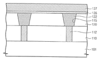
図15、図16及び図17を参照すると、基板101上に下部電極112を含む第1層間絶縁膜110が形成される。前記基板101は第1方向に延長されたワードラインWLを含む。前記ワードラインWLは不純物がドープされたドープラインである。また、前記半導体基板は前記ワードラインWLに接触された選択素子(図示せず)を含む。前記下部電極112は上面が一字形(line type)、弧形(arc type)、円形、四角形又はリング形(ring type)からなる。本実施形態において、前記下部電極112は弧形(arc type)に形成される。前記弧形の下部電極112の上面は前記第2方向への長さが前記第1方向への長さより長い。
Referring to FIGS. 15, 16, and 17, a first
前記下部電極112上には可変抵抗パターン123、例えば、相変化物質パターンが形成される。本実施形態において、前記可変抵抗パターン123は縦断面が四角形である。前記可変抵抗パターン123は前記第1方向に延長されるトレンチ115内に形成される。前記トレンチ115は第2層間絶縁膜120に形成される。従って前記可変抵抗パターン123は前記第2方向に下部電極112上に分離されて形成される。また、前記可変抵抗パターン123は前記第1方向に分離される。即ち、前記可変抵抗パターン123は図16に示したように前記第1方向へ各下部電極112上に分離されて形成される。即ち、前記可変抵抗パターン123は各下部電極112上に島型に形成される。前記可変抵抗パターン123の島型の構造はセル間の干渉現象を緩和させる。
A
前記可変抵抗パターン123上には前記第2方向に延長される上部電極137が形成される。前記上部電極137は前記トレンチ115と交差する。前記可変抵抗パターン123と前記上部電極137との間に拡散防止パターン135が形成される。前記拡散防止パターン135は前記第2方向に延長される。
An
前記可変抵抗パターン123、前記拡散防止パターン135及び前記上部電極137は図16に示したようにアライメントされた側壁138を有する。即ち、前記可変抵抗パターン123は前記上部電極137の側壁に整列された側壁を含む。前記アライメントされた側壁138の間に第3層間絶縁膜140が形成される。
The
前記上部電極137上には前記ワードラインWLと交差するビットラインBLが形成される。前記ビットラインBLは第4層間絶縁膜145のコンタクトプラグ141を通じて前記上部電極137と電気的に接続される。
A bit line BL intersecting with the word line WL is formed on the
本実施形態において、前記上部電極137にアライメントされた前記可変抵抗パターン123の側壁は前記下部電極112とは相対的に遠い距離を置いて配置される。従って、前記可変抵抗パターン123のパターニングの際、発生する損傷による電気特性の劣化が改善される。
In this embodiment, the sidewall of the
以下に、本発明の第2実施形態による可変抵抗メモリ装置の製造方法を説明する。 Hereinafter, a method of manufacturing the variable resistance memory device according to the second embodiment of the present invention will be described.
図18、図20、図22は本発明の第2実施形態による可変抵抗メモリ装置の製造方法を順に示す図15のC−C’線に沿って切断した断面図である。図19、図21、図23は本発明の第2実施形態による可変抵抗メモリ装置の製造方法を順に示す図15のD−D’線に沿って切断した断面図である。 18, 20, and 22 are cross-sectional views taken along the line C-C ′ of FIG. 15 sequentially illustrating the method of manufacturing the variable resistance memory device according to the second embodiment of the present invention. 19, 21 and 23 are cross-sectional views taken along the line D-D 'of FIG.
図15、図18及び図19を参照すると、基板101上に第1層間絶縁膜110を形成する。前記第1層間絶縁膜110に下部電極112が形成される。本実施形態において、前記下部電極112は弧形(arc type)の上面を有するよう形成される。また、弧形の上面を有する前記下部電極112は隣接するメモリセルと互いに対称になる。例えば、弧形の上面を有する前記下部電極112は、隣接する2つのメモリセル領域にわたってオープニング窓を形成し、オープニング窓の内壁に沿って均一に下部電極用の導電膜を蒸着した後に、下部電極用の導電膜をパターニングして2つのメモリセル領域の間の下部電極用の導電膜を除去することによって形成される。一方、下部電極112は弧形の上面を有するとともにU字形で形成される。
Referring to FIGS. 15, 18, and 19, a first
続いて、前記下部電極112上には第2層間絶縁膜120が形成される。前記第2層間絶縁膜120がパターニングされて前記第1方向に延長されるトレンチ115が形成される。前記トレンチ115は前記下部電極112の上面の少なくとも一部を露出する。前記トレンチ115は上部から下部の方に幅がだんだん減少するよう前記第2層間絶縁膜120を異方性エッチングして形成される。
Subsequently, a second
続いて、前記トレンチ115内に可変抵抗ライン122が形成される。前記可変抵抗ライン122は前記第1方向に延長される。また、前記可変抵抗ライン122は前記第2方向に分離されて配置される。前記可変抵抗ライン122は前記第2層間絶縁膜120上に可変抵抗物質膜を蒸着して前記トレンチ115を埋めて、平坦化して形成される。
Subsequently, a
続いて、図15、図20及び図21を参照すると、前記可変抵抗ライン122上には導電膜136が形成される。前記導電膜136は前記下部電極112と同じ物質からなる。
15, 20, and 21, a
また、前記導電膜136と前記可変抵抗ライン122との間に拡散防止膜134が形成される。前記導電膜136及び前記拡散防止膜134はPVD法又はCVD法によって形成される。
In addition, a
前記導電膜136上にはマスクパターン139が形成される。前記マスクパターン139は前記第2方向に延長される。
A
続いて、図15、図22及び図23を参照すると、前記マスクパターン139をマスクにして前記導電膜136、前記拡散防止膜134、前記可変抵抗ライン122がパターニングされる。前記パターニングは乾式エッチングで行なわれる。前記パターニング後、前記マスクパターン139は除去されても良い。前記パターニングによって上部電極137、拡散防止パターン135及び可変抵抗パターン123が形成される。即ち、前記パターニングによって前記上部電極137と前記可変抵抗パターン123が同時に形成される。従って、前記可変抵抗パターン123は前記上部電極137の側壁にアライメントされた側壁を有する。前記パターニングによって前記可変抵抗パターン123は各セル別に分離された島型に形成される。
Subsequently, referring to FIGS. 15, 22 and 23, the
また、図15、図16及び図17を参照すると、前記パターニングによって形成されたリセス領域に第3層間絶縁膜140が形成される。前記第3層間絶縁膜140は前記基板101上に絶縁物質を蒸着した後、前記上部電極137の上面が露出されるよう平坦化して形成される。
Referring to FIGS. 15, 16, and 17, a third
前記上部電極137上には第4層間絶縁膜145を形成し、前記第4層間絶縁膜145をパターニングして前記上部電極137を露出するビットライン用のコンタクトホールを形成する。前記ビットライン用のコンタクトホール内に導電物質を充填してコンタクトプラグ141を形成する。前記コンタクトプラグ141上には前記コンタクトプラグ141と接触するビットラインBLを形成する。前記ビットラインBLは前記上部電極137と平行に前記第2方向へ延長される。
A fourth
以下に、本発明の第3実施形態による可変抵抗メモリ装置及びその製造方法を説明する。 Hereinafter, a variable resistance memory device and a manufacturing method thereof according to a third embodiment of the present invention will be described.
下部電極及び可変抵抗パターンを除いて他の技術構成は第1実施形態と同様である。従って、説明の便宜のために、同じ技術構成に対しては説明を省略する。 Except for the lower electrode and the variable resistance pattern, other technical configurations are the same as those in the first embodiment. Therefore, for convenience of description, description of the same technical configuration is omitted.
図24は本発明の第3実施形態による可変抵抗メモリ装置の平面図である。図25及び図26は本発明の第3実施形態による可変抵抗メモリ装置の断面図である。図25及び図26は各々図24のE−E’線及びF−F’線に沿って切断した断面図である。 FIG. 24 is a plan view of a variable resistance memory device according to a third embodiment of the present invention. 25 and 26 are cross-sectional views of a variable resistance memory device according to a third embodiment of the present invention. 25 and 26 are cross-sectional views taken along lines E-E 'and F-F' in FIG.
図24、図25及び15bを参照すると、基板101上に下部電極112を含む第1層間絶縁膜110が形成される。前記下部電極112は上面が一字形(line type)、弧形(arc type)、円形、四角形又はリング形(ring type)からなる。本実施形態において、前記下部電極112は第1方向と交差する第2方向に一列に配列された一字形(line type)からなる。即ち、前記下部電極112の上面は第2方向に長軸を有し、第1方向に短軸を有するよう形成される。
Referring to FIGS. 24, 25 and 15 b, a first
前記下部電極112上には可変抵抗パターン123、例えば、相変化物質パターンが形成される。前記可変抵抗パターン123は縦断面がU字形、L字形又は四角形からなる。本実施形態において、前記可変抵抗パターン123はL字形に形成される。即ち、前記可変抵抗パターン123は底部と側壁部からなり、実質的にL字形である。前記L字形の可変抵抗パターン123は前記第2方向に隣接するセルの可変抵抗パターンと鏡面対称(mirror symmetry)になるように形成される。前記鏡面対称になる2つのL字形の可変抵抗パターン123は前記第1方向に延長されるトレンチ115の両側壁上に形成される。前記トレンチ115は第2層間絶縁膜120に形成される。従って、前記可変抵抗パターン123は前記第2方向に各下部電極112上に分離されて形成される。また、前記可変抵抗パターン123は前記第1方向にも分離される。即ち、前記可変抵抗パターン123は図26に示したように各下部電極112上に島型に形成される。前記可変抵抗パターン123の島型の構造はセル間の干渉現象を緩和させる。
A
前記可変抵抗パターン123上には熱損失防止パターン128が形成される。前記熱損失防止パターン128は相変化物質が加熱されるとき発生する熱が損失されることを防止する。前記熱損失防止パターン128は前記可変抵抗パターン123上にスペーサ形態で形成される。前記熱損失防止パターン128上にはトレンチ115を埋める絶縁パターン131が形成される。前記絶縁パターン131は酸化膜からなる。
A heat
また、前記可変抵抗パターン123上には前記第2方向に延長される上部電極137が形成される。前記上部電極137は前記トレンチ115と垂直をなす。前記可変抵抗パターン123と前記上部電極137との間に拡散防止パターン135が形成される。前記拡散防止パターン135は第2方向に延長される長さを有する。
An
前記可変抵抗パターン123、前記熱損失防止パターン128、前記拡散防止パターン135及び前記上部電極137は図25に示したようにアライメントされた側壁138を有する。即ち、前記可変抵抗パターン123、前記熱損失防止パターン128、前記拡散防止パターン135は前記上部電極137の側壁に整列された側壁を含む。前記アライメントされた側壁138の間に第3層間絶縁膜140が形成される。
The
また、前記上部電極137上には前記ワードラインWLと交差するビットラインBLが形成される。前記ビットラインBLは第4層間絶縁膜145のコンタクトプラグ141を通じて前記上部電極137と電気的に接続される。
A bit line BL intersecting with the word line WL is formed on the
本実施形態において、前記上部電極137にアライメントされた前記可変抵抗パターン123の側壁は前記下部電極112とは相対的に遠い距離を置いて配置される。従って、前記可変抵抗パターン123のパターニングの際、発生する損傷による電気特性の劣化が改善される。
In this embodiment, the sidewall of the
以下に、本発明の第3実施形態による可変抵抗メモリ装置の製造方法を説明する。 Hereinafter, a method of manufacturing the variable resistance memory device according to the third embodiment of the present invention will be described.
図27、図29、図31、図33は本発明の第3実施形態による可変抵抗メモリ装置の製造方法を順に示す図24のE−E’線に沿って切断した断面図である。図28、図30、図32、図34は本発明の第3実施形態による可変抵抗メモリ装置の製造方法を順に示す図24のF−F’線に沿って切断した断面図である。 27, 29, 31, and 33 are cross-sectional views taken along line E-E 'of FIG. 24 sequentially illustrating a method of manufacturing the variable resistance memory device according to the third embodiment of the present invention. 28, 30, 32, and 34 are cross-sectional views taken along line F-F 'of FIG. 24 sequentially illustrating a method of manufacturing the variable resistance memory device according to the third embodiment of the present invention.
図24、図27及び図28を参照すると、前記基板101上には下部電極112を含む第1層間絶縁膜110が形成される。前記下部電極112上には第2層間絶縁膜120が形成される。前記第2層間絶縁膜120がパターニングされて第1方向に延長されるトレンチ115が形成される。前記トレンチ115は第2方向に隣接する2つの下部電極112上に形成される。前記トレンチ115は前記2つの下部電極112の上面の少なくとも一部を露出する。
Referring to FIGS. 24, 27 and 28, a first
前記トレンチ115の側壁及び底面と前記第2層間絶縁膜120上には可変抵抗物質膜121及び熱損失防止膜126が形成される。
A variable
続いて、図24、図29及び図30を参照すると、前記熱損失防止膜126に対するスペーサを形成する工程を行なって前記トレンチ115の両側壁上に熱損失防止予備パターン127を形成する。前記熱損失防止予備パターン127は前記トレンチ115内から前記可変抵抗物質膜121の一部を露出する。
Next, referring to FIGS. 24, 29, and 30, a process of forming a spacer for the heat
続いて、図24、図31及び図32を参照すると、前記熱損失防止予備パターン127をマスクにして前記可変抵抗物質膜121の露出された部分を除去し、平坦化工程を行なって、互いに分離されたL字形の可変抵抗ライン122を形成する。前記可変抵抗ライン122は前記トレンチの内部側壁上に分離されて形成される。前記平坦化工程の前に前記トレンチ114が完全に埋められるよう絶縁パターン131を形成する。前記平坦化工程の後、不活性気体を用いるプラズマ処理を行なう。
24, 31 and 32, the exposed portion of the variable
前記可変抵抗ライン122、前記熱損失防止予備パターン127及び前記絶縁パターン131上には導電膜136が形成される。前記導電膜136は前記下部電極112と同じ物質からなる。前記導電膜136と前記可変抵抗ライン122との間に拡散防止膜134が形成される。前記導電膜136及び前記拡散防止膜134はPVD法又はCVD法によって形成される。前記導電膜136上にマスクパターン139が形成される。前記マスクパターン139は第2方向に延長される。
A
続いて、図24、図33及び図34を参照すると、前記マスクパターン139をマスクに利用して前記導電膜136、前記拡散防止膜134、前記熱損失防止予備パターン127及び前記可変抵抗ライン122がパターニングされる。前記パターニングは乾式エッチングで行なわれる。前記パターニング後、前記マスクパターン139は除去されても良い。前記パターニングによって上部電極137、拡散防止パターン135、熱損失防止パターン128及び可変抵抗パターン123が形成される。即ち、前記パターニングによって前記上部電極137と前記可変抵抗パターン123が同時に形成される。従って、前記可変抵抗パターン123は前記上部電極137の側壁にアライメントされた側壁を有する。前記パターニングによって前記可変抵抗パターン123は各セル別に分離された島型に形成される。
24, 33, and 34, the
また、図24、図25及び図26を参照すると、前記パターニングによって形成されたリセス領域に第3層間絶縁膜140が形成される。前記上部電極137上には第4層間絶縁膜145が形成され、前記第4層間絶縁膜145をパターニングして前記上部電極137を露出するビットライン用のコンタクトホールを形成する。前記ビットライン用のコンタクトホール内に導電物質を充填してコンタクトプラグ141を形成する。前記コンタクトプラグ141上には前記コンタクトプラグ141と接触するビットラインBLを形成する。前記ビットラインBLは前記上部電極137と平行に第2方向へ延長される長さを有する。
24, 25 and 26, a third
以下に、本発明の第4実施形態による可変抵抗メモリ装置及びその製造方法を説明する。 Hereinafter, a variable resistance memory device and a method for manufacturing the same according to a fourth embodiment of the present invention will be described.
下部電極及び可変抵抗パターンを除いて他の技術構成は第1実施形態と同様である。従って、説明の便宜のために、同じ技術構成に対しては説明を省略する。 Except for the lower electrode and the variable resistance pattern, other technical configurations are the same as those in the first embodiment. Therefore, for convenience of description, description of the same technical configuration is omitted.
図35は本発明の第4実施形態による可変抵抗メモリ装置の平面図である。図36及び図37は本発明の第4実施形態による可変抵抗メモリ装置の断面図である。図36及び図37は各々図35のG−G’線及びH−H’線に沿って切断した断面図である。 FIG. 35 is a plan view of a variable resistance memory device according to a fourth embodiment of the present invention. 36 and 37 are cross-sectional views of a variable resistance memory device according to a fourth embodiment of the present invention. 36 and 37 are cross-sectional views taken along lines G-G ′ and H-H ′ of FIG. 35, respectively.
先ず、図35、図36及び図37を参照すると、基板101上に下部電極112を含む第1層間絶縁膜110が形成される。前記下部電極112は上面が一字形(line type)、弧形(arc type)、円形、四角形又はリング形(ring type)からなる。本実施形態において、前記下部電極112は上面が円形に形成される。
First, referring to FIGS. 35, 36, and 37, a first
前記下部電極112上には可変抵抗ライン122、例えば、相変化物質ラインが形成される。図面において、前記可変抵抗ライン122は縦断面が四角形からなっているが、これに限らず、第1実施形態又は第2実施形態のようにU字形又はL字形に形成しても良い。前記可変抵抗ライン122は前記第1方向に延長されるトレンチ115内に形成される。前記トレンチ115は第2層間絶縁膜120に形成される。従って、前記可変抵抗ライン122は前記第2方向に下部電極112上に分離されて形成される。
A
前記可変抵抗ライン122上には前記第2方向に延長される上部電極137が形成される。前記上部電極137は前記トレンチ115と交差する。前記可変抵抗ライン122と前記上部電極137との間に拡散防止パターン135が形成される。前記拡散防止パターン135は前記第2方向に延長される。
An
前記上部電極137上には前記ワードラインWLと交差するビットラインBLが形成される。前記ビットラインBLは第4層間絶縁膜145のコンタクトプラグ141を通じて前記上部電極137と電気的に接続される。
A bit line BL intersecting with the word line WL is formed on the
以下に、本発明の第4実施形態による可変抵抗メモリ装置の製造方法を説明する。 Hereinafter, a method for manufacturing a variable resistance memory device according to a fourth embodiment of the present invention will be described.
図38、図40、図42は本発明の第4実施形態による可変抵抗メモリ装置の製造方法を順に示す図35のG−G’線に沿って切断した断面図である。図39、図41、図43は本発明の第4実施形態による可変抵抗メモリ装置の製造方法を順に示す図35のH−H’線に沿って切断した断面図である。 38, 40, and 42 are cross-sectional views taken along the line G-G 'of FIG. 35 sequentially illustrating the method of manufacturing the variable resistance memory device according to the fourth embodiment of the invention. 39, 41, and 43 are cross-sectional views taken along the line H-H 'of FIG.
先ず、図35、図38及び図39を参照すると、基板101上に第1層間絶縁膜110を形成する。前記第1層間絶縁膜110に下部電極112が形成される。本実施形態において、前記下部電極112は円形の上面を有するよう形成される。前記下部電極112上には第2層間絶縁膜120が形成される。前記第2層間絶縁膜120がパターニングされて第1方向に延長されるトレンチ115が形成される。前記トレンチ115は前記下部電極112の上面の少なくとも一部を露出する。前記トレンチ115は上部から下部の方にだんだん幅が減少するよう前記第2層間絶縁膜120を異方性エッチングして形成される。
First, referring to FIGS. 35, 38 and 39, a first
前記トレンチ115内に可変抵抗ライン122が形成される。前記可変抵抗ライン122は第1方向に延長される。また、前記可変抵抗ライン122は前記第2方向に分離されて配置される。前記可変抵抗ライン122は前記第2層間絶縁膜120上に可変抵抗物質膜を蒸着した後、平坦化して形成される。
A
続いて、図35、図40及び図41を参照すると、前記可変抵抗ライン122上には導電膜136が形成される。前記導電膜136は前記下部電極112と同じ物質からなる。前記導電膜136と前記可変抵抗ライン122との間に拡散防止膜134が形成される。前記導電膜136及び前記拡散防止膜134はPVD法又はCVD法によって形成される。前記導電膜136上にはマスクパターン139が形成される。前記マスクパターン139は前記第2方向に延長される。
Subsequently, referring to FIGS. 35, 40, and 41, a
続いて、図35、図42及び図43を参照すると、前記マスクパターン139をマスクに利用して前記導電膜136、前記拡散防止膜134がパターニングされる。本実施形態において、前記可変抵抗ライン122は前記導電膜136及び前記拡散防止膜134とともにパターニングされない。前記パターニングは乾式エッチングで行なわれる。前記パターニング後、前記マスクパターン139は除去されても良い。前記パターニングによって上部電極137、拡散防止パターン135が形成される。
Subsequently, referring to FIGS. 35, 42 and 43, the
また、図35、図36及び図37を参照すると、前記パターニングによって形成されたリセス領域に第3層間絶縁膜140が形成される。前記第3層間絶縁膜140は前記基板101上に絶縁物質を蒸着した後、前記上部電極137の上面が露出されるよう平坦化して形成される。前記上部電極137上には第4層間絶縁膜145を形成し、前記第4層間絶縁膜145をパターニングして前記上部電極137を露出するビットライン用のコンタクトホールを形成する。前記ビットライン用のコンタクトホール内に導電物質を充填してコンタクトプラグ141を形成する。前記コンタクトプラグ141上に前記コンタクトプラグ141と接触するビットラインBLを形成する。前記ビットラインBLは前記上部電極137と平行に第2方向へ延長される長さを有する。
Referring to FIGS. 35, 36 and 37, a third
図44は本発明の実施形態による可変抵抗メモリ装置の適用例を示すメモリシステムのブロック図である。 FIG. 44 is a block diagram of a memory system showing an application example of a variable resistance memory device according to an embodiment of the present invention.
図44を参照すると、本発明によるメモリシステム1000は可変抵抗メモリ装置(例えば、PRAM)1100及びメモリコントローラ1200からなる半導体メモリ装置1300、システムバス1450に電気的に接触される中央処理装置1500、ユーザインターフェース1600、電源供給装置1700を含む。
Referring to FIG. 44, a
可変抵抗メモリ装置1100にはユーザインターフェース1600を通じてデータが伝送されたり、中央処理装置1500によって処理されたデータがメモリコントローラ1200を通じて貯蔵されたりするようになっている。可変抵抗メモリ装置1100は半導体ディスク装置(SSD)から構成される。この場合、メモリシステム1000の書き込み速度が画期的に速くなる。
Data is transmitted to the variable
本発明の図面には図示していないが、本発明によるメモリシステム1000には応用チップセット(Application Chipset)、カメライメージプロセッサ(Camera Image Processor:CIS)、モバイルDRAM等がさらに構成される。
Although not shown in the drawings of the present invention, the
また、メモリシステム1000はPDA、ポータブルコンピュータ、ウェブタブレット(web、tablet)、無線電話(wireless phone)、モバイルフォン(mobile phone)、デジタルミュージックプレーヤー(digital music player)、メモリカード(memory card)又は情報を無線環境から送受信できる全ての素子に適用される。
The
なお、本発明による可変抵抗メモリ装置又はメモリシステムは様々な形態でパッケージ化されて実装される。例えば、本発明による可変抵抗メモリ装置又はメモリシステムはPoP(Package on Package)、Ball grid arrays(BGAs)、Chip scale packages(CSPs)、Plastic Leaded Chip Carrier(PLCC)、Plastic Dual In−Line Package(PDIP)、Die in Waffle Pack、Die in Wafer Form、Chip On Board(COB)、Ceramic Dual In−LinePackage(CERDIP)、Plastic Metric Quad Flat Pack(MQFP)、Thin Quad Flatpack(TQFP)、Small Outline(SOIC)、Shrink Small Outline Package(SSOP)、Thin Small Outline(TSOP)、Thin Quad Flatpack(TQFP)、System In Package(SIP)、Multi Chip Package(MCP)、Wafer−level Fabricated Package(WFP)、Wafer−Level Processed Stack Package(WSP)等のような方式でパッケージ化されて実装される。 The variable resistance memory device or memory system according to the present invention is packaged and mounted in various forms. For example, the variable resistance memory device or the memory system according to the present invention includes PoP (Package on Package), Ball grid arrays (BGAs), Chip scale packages (CSPs), Plastic Leaded Chip Carrier (PLCC), and Plastic-In-DneP ), Die in Waffle Pack, Die in Wafer Form, Chip On Board (COB), Ceramic Dual In-Line Package (CERDIP), Plastic Metric Quad Flat Pack (MQP) , Shrink Small Outline Package (SSOP), Thin Small Outline (TSOP), Thin Quad Flatpack (TQFP), System In Package (SIP), MultiChip Package (MCP), V It is packaged and mounted by a method such as Stack Package (WSP).
以上、添付の図面を参照して本発明の実施形態等を説明したが、本発明が属する技術分野で通常の知識を持つ者であれば、本発明の技術思想、特徴等を変更しなくて異なる形態で実施することができるだろう。従って、本発明の実施形態等により本発明が限定されてはならない。 The embodiments of the present invention have been described above with reference to the accompanying drawings. However, those who have ordinary knowledge in the technical field to which the present invention belongs need not change the technical idea, features, etc. of the present invention. It could be implemented in different forms. Therefore, the present invention should not be limited by the embodiments of the present invention.
101 基板
110 第1層間絶縁膜
112 下部電極
115 トレンチ
120 第2層間絶縁膜
122 可変抵抗ライン
123 可変抵抗パターン
128 熱損失防止パターン
131 絶縁パターン
135 拡散防止パターン
137 上部電極
138 側壁
140 第3層間絶縁膜
141 コンタクトプラグ
145 第4層間絶縁膜
1000 メモリシステム
1100 可変抵抗メモリ装置
1200 メモリコントローラ
1300 半導体メモリ装置
1450 システムバス
1500 中央処理装置
1600 ユーザインターフェース
1700 電源供給装置
101 substrate
110 First interlayer insulating film
112
122 Variable resistance line
123 Variable resistance pattern
128 Heat
140 Third
1000
Claims (10)
前記基板上の複数の下部電極と
複数の前記下部電極を露出し、第1方向に延長されるトレンチを含む第1層間絶縁膜と、
前記第1層間絶縁膜上に形成され、前記第1方向と交差する第2方向に延長される上部電極と、
前記トレンチ内に形成され、前記上部電極の側壁にアライメントされる側壁を含む複数の可変抵抗パターンを有することを特徴とする可変抵抗メモリ装置。 A substrate,
A first interlayer insulating film including a plurality of lower electrodes on the substrate, a plurality of the lower electrodes exposed, and a trench extending in a first direction;
An upper electrode formed on the first interlayer insulating film and extending in a second direction intersecting the first direction;
A variable resistance memory device comprising: a plurality of variable resistance patterns including sidewalls formed in the trench and aligned with sidewalls of the upper electrode.
前記基板上の複数の下部電極と、
前記下部電極上に形成され、第1方向に延長される複数の可変抵抗ラインと、
前記可変抵抗ライン上に形成され、前記第1方向と交差する第2方向に延長される上部電極を含むことを特徴とする可変抵抗メモリ装置。 A substrate,
A plurality of lower electrodes on the substrate;
A plurality of variable resistance lines formed on the lower electrode and extending in a first direction;
A variable resistance memory device, comprising: an upper electrode formed on the variable resistance line and extending in a second direction intersecting the first direction.
前記下部電極上に第1方向に延長される複数の可変抵抗ラインを形成し、
前記可変抵抗ライン上に、前記第1方向と交差する第2方向に延長される上部電極を形成することを特徴とする可変抵抗メモリ装置の製造方法。 Forming a plurality of lower electrodes on the substrate;
Forming a plurality of variable resistance lines extending in the first direction on the lower electrode;
A method of manufacturing a variable resistance memory device, comprising: forming an upper electrode extending in a second direction intersecting the first direction on the variable resistance line.
前記可変抵抗ライン上に導電膜を形成し、
前記導電膜上に前記第2方向に延長されるマスクパターンを形成し、
前記マスクパターンによって前記導電膜を前記第2方向に延長されるようにパターニングすることを特徴とする請求項5に記載の可変抵抗メモリ装置の製造方法。 Forming the upper electrode comprises:
Forming a conductive film on the variable resistance line;
Forming a mask pattern extending in the second direction on the conductive film;
6. The method of manufacturing a variable resistance memory device according to claim 5, wherein the conductive film is patterned by the mask pattern so as to extend in the second direction.
前記下部電極上に層間絶縁膜を形成し、
前記層間絶縁膜に前記第1方向に延長され、前記下部電極の上面の少なくとも一部を露出するトレンチを形成し、
前記トレンチ上に可変抵抗物質膜を形成することを特徴とする請求項5に記載の可変抵抗メモリ装置の製造方法。 Forming the variable resistance line includes
Forming an interlayer insulating film on the lower electrode;
Forming a trench extending in the first direction in the interlayer insulating film and exposing at least a part of an upper surface of the lower electrode;
6. The method of manufacturing a variable resistance memory device according to claim 5, wherein a variable resistance material film is formed on the trench.
Applications Claiming Priority (2)
| Application Number | Priority Date | Filing Date | Title |
|---|---|---|---|
| KR1020090128097A KR101617381B1 (en) | 2009-12-21 | 2009-12-21 | Resistance variable memory device and method for forming the same |
| KR10-2009-0128097 | 2009-12-21 |
Publications (2)
| Publication Number | Publication Date |
|---|---|
| JP2011129934A true JP2011129934A (en) | 2011-06-30 |
| JP5660882B2 JP5660882B2 (en) | 2015-01-28 |
Family
ID=44149770
Family Applications (1)
| Application Number | Title | Priority Date | Filing Date |
|---|---|---|---|
| JP2010284395A Active JP5660882B2 (en) | 2009-12-21 | 2010-12-21 | Variable resistance memory device and manufacturing method thereof |
Country Status (4)
| Country | Link |
|---|---|
| US (2) | US8552412B2 (en) |
| JP (1) | JP5660882B2 (en) |
| KR (1) | KR101617381B1 (en) |
| CN (1) | CN102104055B (en) |
Families Citing this family (32)
| Publication number | Priority date | Publication date | Assignee | Title |
|---|---|---|---|---|
| JP5607143B2 (en) * | 2009-04-21 | 2014-10-15 | マーベル ワールド トレード リミテッド | COMMUNICATION METHOD, COMMUNICATION DEVICE, MOBILE COMMUNICATION TERMINAL, CHIPSET, AND COMMUNICATION SYSTEM |
| KR20110076394A (en) * | 2009-12-29 | 2011-07-06 | 삼성전자주식회사 | Phase change memory device |
| KR20120104031A (en) * | 2011-03-11 | 2012-09-20 | 삼성전자주식회사 | Phase change material layer, method of forming a phase change layer, phase change memory device and method of manufacturing a phase change memory device |
| KR101872949B1 (en) * | 2011-05-17 | 2018-07-02 | 삼성전자주식회사 | Phase change memory device and method of manufacturing the same |
| JP5611903B2 (en) * | 2011-08-09 | 2014-10-22 | 株式会社東芝 | Resistance change memory |
| US8599599B2 (en) * | 2011-09-01 | 2013-12-03 | Micron Technology, Inc. | Method, system, and device for phase change memory switch wall cell with approximately horizontal electrode contact |
| CN103296050B (en) * | 2012-03-02 | 2015-10-14 | 中芯国际集成电路制造(上海)有限公司 | Phase transition storage and manufacture method thereof |
| KR101900853B1 (en) * | 2012-04-13 | 2018-09-20 | 삼성전자주식회사 | Variable Resistance memory device and method of forming the same |
| KR101994280B1 (en) | 2012-07-26 | 2019-07-01 | 에스케이하이닉스 주식회사 | Resistance variable memory device and method for manufacturing the same |
| JP6014521B2 (en) * | 2013-03-11 | 2016-10-25 | 株式会社日立製作所 | Phase change memory and semiconductor recording / reproducing apparatus |
| US9118006B1 (en) * | 2014-08-12 | 2015-08-25 | Boise State University | Carbon-chalcogenide variable resistance memory device |
| KR20160131180A (en) * | 2015-05-06 | 2016-11-16 | 에스케이하이닉스 주식회사 | Electronic device and method for operation the same |
| US10424619B2 (en) * | 2016-01-13 | 2019-09-24 | Samsung Electronics Co., Ltd. | Variable resistance memory devices and methods of manufacturing the same |
| US9660189B1 (en) * | 2016-02-29 | 2017-05-23 | Arm Ltd. | Barrier layer for correlated electron material |
| CN107204397B (en) * | 2016-03-18 | 2019-06-21 | 中国科学院微电子研究所 | Selection device for bipolar resistive memory and method of making the same |
| KR102673120B1 (en) * | 2016-12-05 | 2024-06-05 | 삼성전자주식회사 | Semiconductor device and method for fabricating the same |
| US9928893B1 (en) * | 2017-06-05 | 2018-03-27 | Xerox Corporation | Circular printed memory system and method having robustness to orientation |
| KR102368428B1 (en) * | 2017-06-29 | 2022-03-02 | 삼성전자주식회사 | Variable resistance memory device and method of forming the same |
| KR102357987B1 (en) * | 2017-07-14 | 2022-02-04 | 삼성전자주식회사 | Variable resistance memory device and method of forming the same |
| US11289647B2 (en) * | 2017-10-19 | 2022-03-29 | Taiwan Semiconductor Manufacturing Co., Ltd. | Resistive random access memory device |
| US20200013951A1 (en) | 2018-07-06 | 2020-01-09 | Taiwan Semiconductor Manufacturing Co., Ltd. | Pcram structure |
| JP2020027818A (en) * | 2018-08-09 | 2020-02-20 | キオクシア株式会社 | Semiconductor storage device |
| US11158788B2 (en) * | 2018-10-30 | 2021-10-26 | International Business Machines Corporation | Atomic layer deposition and physical vapor deposition bilayer for additive patterning |
| KR102675357B1 (en) * | 2019-01-08 | 2024-06-17 | 삼성전자주식회사 | Variable resistance memory device and method of forming the same |
| US11183503B2 (en) * | 2019-07-31 | 2021-11-23 | Taiwan Semiconductor Manufacturing Company, Ltd. | Memory cell having top and bottom electrodes defining recesses |
| CN113013327B (en) * | 2019-12-19 | 2023-11-21 | 华邦电子股份有限公司 | Resistive random access memory and manufacturing method thereof |
| CN111146339B (en) * | 2019-12-19 | 2023-01-31 | 上海集成电路研发中心有限公司 | A kind of phase-change memory unit and preparation method thereof |
| TWI716235B (en) * | 2019-12-24 | 2021-01-11 | 華邦電子股份有限公司 | Resistive random access memory and manufacturing method thereof |
| CN113078257B (en) * | 2020-01-03 | 2023-09-12 | 华邦电子股份有限公司 | Resistive random access memory and manufacturing method thereof |
| CN113192929B (en) * | 2020-01-14 | 2023-07-25 | 联华电子股份有限公司 | Resistive memory structure and manufacturing method thereof |
| EP3890024B1 (en) * | 2020-03-30 | 2024-05-01 | STMicroelectronics (Crolles 2) SAS | Electronic chip with two phase change memories and method of fabrication |
| CN112271254B (en) * | 2020-10-27 | 2021-12-28 | 长江先进存储产业创新中心有限责任公司 | Phase change memory and manufacturing method thereof |
Citations (3)
| Publication number | Priority date | Publication date | Assignee | Title |
|---|---|---|---|---|
| US8004A (en) * | 1851-03-25 | Francis b | ||
| JP2006074028A (en) * | 2004-08-31 | 2006-03-16 | Samsung Electronics Co Ltd | Method for manufacturing phase change memory element having small contacts |
| JP2008263159A (en) * | 2007-03-20 | 2008-10-30 | Sharp Corp | Method for manufacturing variable resistance element |
Family Cites Families (35)
| Publication number | Priority date | Publication date | Assignee | Title |
|---|---|---|---|---|
| US5751012A (en) | 1995-06-07 | 1998-05-12 | Micron Technology, Inc. | Polysilicon pillar diode for use in a non-volatile memory cell |
| US5831276A (en) | 1995-06-07 | 1998-11-03 | Micron Technology, Inc. | Three-dimensional container diode for use with multi-state material in a non-volatile memory cell |
| US6586761B2 (en) | 2001-09-07 | 2003-07-01 | Intel Corporation | Phase change material memory device |
| US7319057B2 (en) | 2001-10-30 | 2008-01-15 | Ovonyx, Inc. | Phase change material memory device |
| KR20040047272A (en) | 2002-11-29 | 2004-06-05 | 삼성전자주식회사 | Phase changing type semiconductor memory device |
| US6858542B2 (en) | 2003-01-17 | 2005-02-22 | Freescale Semiconductor, Inc. | Semiconductor fabrication method for making small features |
| US7009694B2 (en) | 2004-05-28 | 2006-03-07 | International Business Machines Corporation | Indirect switching and sensing of phase change memory cells |
| US7364935B2 (en) | 2004-10-29 | 2008-04-29 | Macronix International Co., Ltd. | Common word line edge contact phase-change memory |
| US7238959B2 (en) | 2004-11-01 | 2007-07-03 | Silicon Storage Technology, Inc. | Phase change memory device employing thermally insulating voids and sloped trench, and a method of making same |
| US20060097341A1 (en) | 2004-11-05 | 2006-05-11 | Fabio Pellizzer | Forming phase change memory cell with microtrenches |
| KR100657911B1 (en) | 2004-11-10 | 2006-12-14 | 삼성전자주식회사 | Nonvolatile Memory Device with One Resistor and One Diode |
| KR100707182B1 (en) | 2005-02-18 | 2007-04-13 | 삼성전자주식회사 | Phase change memory device and manufacturing method |
| KR100657956B1 (en) | 2005-04-06 | 2006-12-14 | 삼성전자주식회사 | Multi-value resistor memory device and its manufacture and operation method |
| KR100842903B1 (en) | 2005-06-10 | 2008-07-02 | 주식회사 하이닉스반도체 | Phase change memory device and manufacturing method thereof |
| JP4560818B2 (en) | 2005-07-22 | 2010-10-13 | エルピーダメモリ株式会社 | Semiconductor device and manufacturing method thereof |
| US7589364B2 (en) | 2005-11-02 | 2009-09-15 | Elpida Memory, Inc. | Electrically rewritable non-volatile memory element and method of manufacturing the same |
| US7397060B2 (en) | 2005-11-14 | 2008-07-08 | Macronix International Co., Ltd. | Pipe shaped phase change memory |
| US20070111429A1 (en) | 2005-11-14 | 2007-05-17 | Macronix International Co., Ltd. | Method of manufacturing a pipe shaped phase change memory |
| US7515455B2 (en) | 2006-03-17 | 2009-04-07 | Qimonda North America Corp. | High density memory array for low power application |
| JP4777820B2 (en) | 2006-04-20 | 2011-09-21 | エルピーダメモリ株式会社 | Semiconductor memory device and manufacturing method thereof |
| TWI305678B (en) | 2006-08-14 | 2009-01-21 | Ind Tech Res Inst | Phase-change memory and fabricating method thereof |
| US20080048293A1 (en) | 2006-08-22 | 2008-02-28 | Samsung Electronics Co., Ltd. | Semiconductor device having heating structure and method of forming the same |
| JP4437299B2 (en) | 2006-08-25 | 2010-03-24 | エルピーダメモリ株式会社 | Semiconductor device and manufacturing method thereof |
| KR100858083B1 (en) | 2006-10-18 | 2008-09-10 | 삼성전자주식회사 | A phase change memory device having a large contact area between a lower electrode contact layer and a phase change layer and a method of manufacturing the same |
| KR100827661B1 (en) | 2006-10-31 | 2008-05-07 | 삼성전자주식회사 | Phase change memory device having a double bottom electrode and method of manufacturing the same |
| US7663135B2 (en) | 2007-01-31 | 2010-02-16 | Macronix International Co., Ltd. | Memory cell having a side electrode contact |
| US7800093B2 (en) | 2007-02-01 | 2010-09-21 | Qimonda North America Corp. | Resistive memory including buried word lines |
| US7729162B2 (en) | 2007-10-09 | 2010-06-01 | Ovonyx, Inc. | Semiconductor phase change memory using multiple phase change layers |
| KR20090097362A (en) * | 2008-03-11 | 2009-09-16 | 삼성전자주식회사 | Resistor Memory Device and Formation Method |
| KR100979755B1 (en) * | 2008-03-28 | 2010-09-02 | 삼성전자주식회사 | Phase change memory device and manufacturing methods thereof |
| US7919768B2 (en) | 2008-07-11 | 2011-04-05 | Industrial Technology Research Institute | Phase-change memory element |
| KR101486984B1 (en) * | 2008-10-30 | 2015-01-30 | 삼성전자주식회사 | Resistance changeable memory device and method of forming thereof |
| CN101459129B (en) * | 2008-12-18 | 2010-10-27 | 中国科学院上海微系统与信息技术研究所 | Self-aligned Schottky diode and method for manufacturing corresponding resistance switching memory |
| CN101436607B (en) * | 2008-12-25 | 2011-11-16 | 中国科学院上海微系统与信息技术研究所 | Electric resistance transition memory and manufacturing method thereof |
| US8377741B2 (en) | 2008-12-30 | 2013-02-19 | Stmicroelectronics S.R.L. | Self-heating phase change memory cell architecture |
-
2009
- 2009-12-21 KR KR1020090128097A patent/KR101617381B1/en active Active
-
2010
- 2010-12-20 US US12/973,124 patent/US8552412B2/en active Active
- 2010-12-21 JP JP2010284395A patent/JP5660882B2/en active Active
- 2010-12-21 CN CN201010598271.3A patent/CN102104055B/en active Active
-
2013
- 2013-09-20 US US14/032,997 patent/US8962438B2/en active Active
Patent Citations (3)
| Publication number | Priority date | Publication date | Assignee | Title |
|---|---|---|---|---|
| US8004A (en) * | 1851-03-25 | Francis b | ||
| JP2006074028A (en) * | 2004-08-31 | 2006-03-16 | Samsung Electronics Co Ltd | Method for manufacturing phase change memory element having small contacts |
| JP2008263159A (en) * | 2007-03-20 | 2008-10-30 | Sharp Corp | Method for manufacturing variable resistance element |
Also Published As
| Publication number | Publication date |
|---|---|
| US8962438B2 (en) | 2015-02-24 |
| KR20110071506A (en) | 2011-06-29 |
| JP5660882B2 (en) | 2015-01-28 |
| CN102104055B (en) | 2015-04-08 |
| US20110147692A1 (en) | 2011-06-23 |
| CN102104055A (en) | 2011-06-22 |
| US20140024195A1 (en) | 2014-01-23 |
| KR101617381B1 (en) | 2016-05-02 |
| US8552412B2 (en) | 2013-10-08 |
Similar Documents
| Publication | Publication Date | Title |
|---|---|---|
| JP5660882B2 (en) | Variable resistance memory device and manufacturing method thereof | |
| US20100051896A1 (en) | Variable resistance memory device using a channel-shaped variable resistance pattern | |
| US11251369B2 (en) | Semiconductor constructions | |
| CN103811513B (en) | Semiconductor devices and its manufacture method | |
| US20130299766A1 (en) | Variable resistance memory device and methods of forming the same | |
| US20100176365A1 (en) | Resistance variable memory devices and methods of fabricating the same | |
| KR20110090583A (en) | Phase change memory device and forming method thereof | |
| US20080272355A1 (en) | Phase change memory device and method for forming the same | |
| US8133758B2 (en) | Method of fabricating phase-change memory device having TiC layer | |
| KR20200018133A (en) | Variable resistance memory devices | |
| US8810003B2 (en) | Semiconductor device and method of fabricating the same | |
| KR20120135089A (en) | Memory devices and method of manufacturing the same | |
| US11950517B2 (en) | Three-dimensional semiconductor memory devices | |
| US20090206318A1 (en) | Nonvolatile memory device and method of manufacturing the same | |
| US8853660B2 (en) | Semiconductor memory devices having lower and upper interconnections, selection components and memory components | |
| KR20210069164A (en) | Variable resistance memory device and method of forming the same | |
| US20100124800A1 (en) | Variable resistance memory device, method of fabricating the same, and memory system including the same | |
| US11393977B2 (en) | Semiconductor device including vertical structures and a method of manufacturing the same | |
| KR101077158B1 (en) | a Method of manufacturing Phase Change RAM | |
| KR20100027949A (en) | Variable resistance memory device and method of manufacturing the same | |
| KR20080114024A (en) | Phase change memory device and manufacturing method thereof | |
| KR20080062076A (en) | Formation method of phase change memory device | |
| KR20130087197A (en) | Method for manufacturing phase-change random access memory device |
Legal Events
| Date | Code | Title | Description |
|---|---|---|---|
| A621 | Written request for application examination |
Free format text: JAPANESE INTERMEDIATE CODE: A621 Effective date: 20130827 |
|
| A977 | Report on retrieval |
Free format text: JAPANESE INTERMEDIATE CODE: A971007 Effective date: 20140625 |
|
| A131 | Notification of reasons for refusal |
Free format text: JAPANESE INTERMEDIATE CODE: A131 Effective date: 20140708 |
|
| A521 | Request for written amendment filed |
Free format text: JAPANESE INTERMEDIATE CODE: A523 Effective date: 20140930 |
|
| TRDD | Decision of grant or rejection written | ||
| A01 | Written decision to grant a patent or to grant a registration (utility model) |
Free format text: JAPANESE INTERMEDIATE CODE: A01 Effective date: 20141111 |
|
| A61 | First payment of annual fees (during grant procedure) |
Free format text: JAPANESE INTERMEDIATE CODE: A61 Effective date: 20141202 |
|
| R150 | Certificate of patent or registration of utility model |
Ref document number: 5660882 Country of ref document: JP Free format text: JAPANESE INTERMEDIATE CODE: R150 |
|
| R250 | Receipt of annual fees |
Free format text: JAPANESE INTERMEDIATE CODE: R250 |
|
| R250 | Receipt of annual fees |
Free format text: JAPANESE INTERMEDIATE CODE: R250 |
|
| R250 | Receipt of annual fees |
Free format text: JAPANESE INTERMEDIATE CODE: R250 |
|
| R250 | Receipt of annual fees |
Free format text: JAPANESE INTERMEDIATE CODE: R250 |
|
| R250 | Receipt of annual fees |
Free format text: JAPANESE INTERMEDIATE CODE: R250 |
|
| R250 | Receipt of annual fees |
Free format text: JAPANESE INTERMEDIATE CODE: R250 |
|
| R250 | Receipt of annual fees |
Free format text: JAPANESE INTERMEDIATE CODE: R250 |
|
| R250 | Receipt of annual fees |
Free format text: JAPANESE INTERMEDIATE CODE: R250 |
|
| R250 | Receipt of annual fees |
Free format text: JAPANESE INTERMEDIATE CODE: R250 |