JP2011237355A - Film thickness measuring method and film thickness measuring apparatus - Google Patents
Film thickness measuring method and film thickness measuring apparatus Download PDFInfo
- Publication number
- JP2011237355A JP2011237355A JP2010110750A JP2010110750A JP2011237355A JP 2011237355 A JP2011237355 A JP 2011237355A JP 2010110750 A JP2010110750 A JP 2010110750A JP 2010110750 A JP2010110750 A JP 2010110750A JP 2011237355 A JP2011237355 A JP 2011237355A
- Authority
- JP
- Japan
- Prior art keywords
- light
- film thickness
- film
- measured
- substrate
- Prior art date
- Legal status (The legal status is an assumption and is not a legal conclusion. Google has not performed a legal analysis and makes no representation as to the accuracy of the status listed.)
- Pending
Links
Images

Landscapes
- Length Measuring Devices By Optical Means (AREA)
- Manufacture Of Electron Tubes, Discharge Lamp Vessels, Lead-In Wires, And The Like (AREA)
- Gas-Filled Discharge Tubes (AREA)
Abstract
Description
本発明は、基材に形成した被測定対象膜の膜厚を非破壊、非接触で測定する膜厚測定装置に関し、特にプラズマディスプレイパネルの保護膜の膜厚測定に好適な膜厚測定方法と膜厚測定装置に関する。 The present invention relates to a film thickness measuring apparatus that measures the film thickness of a film to be measured formed on a substrate in a non-destructive and non-contact manner, and in particular, a film thickness measuring method suitable for measuring a film thickness of a protective film of a plasma display panel and The present invention relates to a film thickness measuring device.
近年、大画面、高精細の画面表示装置としてプラズマディスプレイパネル(以下、「PDP」と略記する)を用いた画像表示装置が開発生産されている。PDPとして代表的な交流面放電型PDPは、前面基板と背面基板とからなり、それらが対向配置されて周囲が封着されるとともに内部に多数の放電セルが形成された構成になっている。 In recent years, an image display device using a plasma display panel (hereinafter abbreviated as “PDP”) is developed and produced as a large-screen, high-definition screen display device. A typical AC surface discharge type PDP as a PDP is composed of a front substrate and a back substrate, which are arranged to face each other and sealed around each other, and a large number of discharge cells are formed inside.
PDPのガラス基板などよりなる前面基板には誘電体層が形成され、さらに誘電体層を覆って保護膜が形成されている。保護膜は放電で生じるイオン衝撃から誘電体層を保護するとともに、二次電子を放出して駆動電圧を低下させる機能を有している。保護膜の材料としては、耐イオン衝撃性の高い酸化マグネシウム(MgO)膜が用いられ、一般的には真空蒸着法などにより製膜される。このような真空蒸着法による製膜では、蒸着された膜厚が放電特性に大きな影響を及ぼすため、誘電体層上に形成された保護膜の膜厚を高精度に自動測定して製品の品質を確保することが求められている。 A dielectric layer is formed on a front substrate made of a glass substrate of PDP, and a protective film is further formed to cover the dielectric layer. The protective film has a function of protecting the dielectric layer from ion bombardment caused by electric discharge and reducing the driving voltage by emitting secondary electrons. As a material of the protective film, a magnesium oxide (MgO) film having high ion impact resistance is used, and is generally formed by a vacuum deposition method or the like. In film formation by such a vacuum deposition method, the deposited film thickness has a great influence on the discharge characteristics. Therefore, the film thickness of the protective film formed on the dielectric layer is automatically measured with high accuracy and the product quality Is required to ensure.
このような保護膜の膜厚を、製造工程においてインラインで測定する方法として分光干渉法を用いた方法が一般的である。例えば、特許文献1には、被測定対象膜に垂直に光を照射し、被測定対象膜の表面と被測定対象膜とその基板との界面とでそれぞれ反射した光の干渉光を、分光器を通して分離して得られた干渉波長から膜厚を測定する方法とその膜厚測定装置が開示されている。
As a method for measuring the thickness of such a protective film in-line in a manufacturing process, a method using a spectral interference method is generally used. For example, in
しかしながら、近年のPDPにおいては、発光効率の更なる向上が求められ、そのために、保護膜の下に形成した誘電体層の比誘電率を小さくするようにしている。その結果、誘電体層と、誘電体層の上に形成される酸化マグネシウムの保護膜との屈折率の差が非常に小さくなってきている。このため、非測定対象膜である保護膜の膜厚を測定する際に、保護膜と誘電体層との界面での反射強度の差が弱まって干渉信号の強度が小さくなり、保護膜の膜厚を精度良く測定できないという課題が発生する。 However, in recent PDPs, further improvement in light emission efficiency is required. For this purpose, the dielectric constant of the dielectric layer formed under the protective film is reduced. As a result, the difference in refractive index between the dielectric layer and the magnesium oxide protective film formed on the dielectric layer has become very small. For this reason, when measuring the film thickness of the protective film that is a non-measurement target film, the difference in reflection intensity at the interface between the protective film and the dielectric layer is weakened, and the intensity of the interference signal is reduced. The problem that thickness cannot be measured accurately occurs.
本発明は、このような課題を解決し、非測定対象膜との屈折率の差が小さい基材の上に形成された非測定対象膜の膜厚を精度良くインラインで測定できる膜厚測定方法とその膜厚測定装置を提供することを目的とする。 The present invention solves such problems, and a film thickness measuring method capable of accurately measuring in-line the film thickness of a non-measurement target film formed on a substrate having a small difference in refractive index from the non-measurement target film. And an apparatus for measuring the film thickness.
上記の目的を達成するために、本発明の膜厚測定方法は、基板上に形成された被測定対象膜の膜厚を測定する膜厚測定方法であって、被測定対象膜の表面に45度以上の入射角度を有して光源からパルス光を照射する光照射ステップと、表面から反射した表面反射光と基板と被測定対象膜との界面から反射した界面反射光とによって形成された干渉光を分光する分光ステップと、パルス光の位相と周期の情報に基づいて光源からの信号と外乱光によるノイズとを分離する分離ステップと、分光ステップで分光された光を検知する光検出ステップとを備えている。 In order to achieve the above object, a film thickness measuring method of the present invention is a film thickness measuring method for measuring a film thickness of a film to be measured formed on a substrate, and is provided on the surface of the film to be measured. Interference formed by a light irradiation step of irradiating pulsed light from a light source with an incident angle of more than 90 degrees, and surface reflected light reflected from the surface and interface reflected light reflected from the interface between the substrate and the film to be measured A spectroscopic step for splitting light; a separation step for separating a signal from the light source and noise due to disturbance light based on information on the phase and period of the pulsed light; and a light detection step for detecting light dispersed in the spectroscopic step; It has.
このような方法によれば、基板と被測定対象膜との界面からの反射強度を大きくすることができ、非測定対象膜との屈折率の差が小さい基板の上に形成された非測定対象膜の膜厚測定を、ノイズの影響を低減しながら高い測定精度で測定することができる。 According to such a method, the reflection intensity from the interface between the substrate and the film to be measured can be increased, and the non-measurement object formed on the substrate having a small difference in refractive index from the non-measurement object film. The film thickness can be measured with high measurement accuracy while reducing the influence of noise.
さらに、パルス光が近紫外光を含む光であることが望ましい。このような方法によれば、膜厚測定をより高精度に行うことができる。 Further, it is desirable that the pulsed light is light including near ultraviolet light. According to such a method, the film thickness can be measured with higher accuracy.
さらに、光検出ステップに入射する前の光をビームスプリッターで分割して参照光とし、参照光を用いて波長毎の光強度を補正する補正ステップを備えることが望ましい。このような方法によれば、干渉信号のピークを精度よく認識できるため、測定精度をさらに高めることができる。 Furthermore, it is desirable to provide a correction step of correcting the light intensity for each wavelength using the reference light by dividing the light before entering the light detection step with a beam splitter to be the reference light. According to such a method, since the peak of the interference signal can be recognized with high accuracy, the measurement accuracy can be further improved.
さらに、光検出ステップで検知した波長と光強度の関係を波数と光強度の関係に換算した後に周期情報に変換する変換ステップをさらに備え、被測定対象膜を測定して得られる周期情報と基板を測定して得られる周期情報との差分を算出する演算ステップを備えることが望ましい。このような構成によれば、外乱光などによるノイズの影響を低減して測定精度をより高めることができる。 Furthermore, it further includes a conversion step of converting the relationship between the wavelength and the light intensity detected in the light detection step into a relationship between the wave number and the light intensity, and then converting the relationship into period information, and the period information obtained by measuring the measurement target film and the substrate It is desirable to include a calculation step for calculating a difference from the period information obtained by measuring the. According to such a configuration, the measurement accuracy can be further improved by reducing the influence of noise caused by disturbance light or the like.
また、本発明の膜厚測定装置は、基板上に形成された被測定対象膜の膜厚を測定する膜厚測定装置であって、被測定対象膜の表面に45度以上の入射角度を有してパルス光を照射する光源と、表面から反射した表面反射光と基板と被測定対象膜との界面から反射した界面反射光とによって形成された干渉光を分光する分光器と、パルス光の位相と周期の情報に基づいて光源からの信号と外乱光によるノイズとを分離するノイズ分離器と、分光器で分光された光を検知する光検出器とを備えている。 The film thickness measuring apparatus of the present invention is a film thickness measuring apparatus for measuring the film thickness of a film to be measured formed on a substrate, and has an incident angle of 45 degrees or more on the surface of the film to be measured. A light source that emits pulsed light, a spectroscope that separates interference light formed by the surface reflected light reflected from the surface and the interface reflected light reflected from the interface between the substrate and the film to be measured, A noise separator that separates a signal from the light source and noise caused by disturbance light based on phase and period information, and a photodetector that detects light dispersed by the spectroscope.
このような構成によれば、基板と被測定対象膜との界面からの反射強度を大きくすることができ、非測定対象膜との屈折率の差が小さい基板の上に形成された非測定対象膜の膜厚測定を、ノイズの影響を低減しながら高い測定精度で測定することができる。 According to such a configuration, the reflection intensity from the interface between the substrate and the film to be measured can be increased, and the non-measurement target formed on the substrate having a small difference in refractive index from the non-measurement target film. The film thickness can be measured with high measurement accuracy while reducing the influence of noise.
さらに、光源が近紫外光を含む光を照射する光源であることが望ましい。このような構成によれば、膜厚測定をより高精度に行うことができる。 Furthermore, it is desirable that the light source is a light source that emits light including near-ultraviolet light. According to such a configuration, the film thickness can be measured with higher accuracy.
さらに、光検出器に入射する前の光を分割して参照光とするビームスプリッターと、参照光を用いて波長毎の光強度を補正する補正部とを備えることが望ましい。このような構成によれば、干渉信号のピークを精度よく認識できるため、測定精度をさらに高めることができる。 Furthermore, it is desirable to include a beam splitter that divides the light before entering the photodetector to obtain reference light, and a correction unit that corrects the light intensity for each wavelength using the reference light. According to such a configuration, since the peak of the interference signal can be recognized with high accuracy, the measurement accuracy can be further improved.
さらに、光検出器で取得した波長と光強度の関係を波数と光強度の関係に換算した後に周期情報に変換する変換部をさらに備え、被測定対象膜を測定して得られる周期情報と基板を測定して得られる周期情報との差分を算出する演算部を備えることが望ましい。このような構成によれば、外乱光などによるノイズの影響を低減して測定精度をより高めることができる。 Further, the substrate further includes a conversion unit that converts the relationship between the wavelength and the light intensity acquired by the photodetector into the relationship between the wave number and the light intensity and then converts the relationship into the period information, and the period information and the substrate obtained by measuring the film to be measured It is desirable to include a calculation unit that calculates the difference from the period information obtained by measuring the. According to such a configuration, the measurement accuracy can be further improved by reducing the influence of noise caused by disturbance light or the like.
以上のように、本発明の膜厚測定方法および膜厚測定装置によれば、基板との屈折率の差が小さい非測定対象膜との屈折率の差が小さい基板上に形成された非測定対象膜の膜厚を、高精度に測定することができる。 As described above, according to the film thickness measuring method and the film thickness measuring apparatus of the present invention, the non-measurement formed on the substrate having a small difference in refractive index from the non-measurement target film having a small difference in refractive index from the substrate. The film thickness of the target film can be measured with high accuracy.
以下、本発明の実施の形態における膜厚測定方法と膜厚測定装置について、PDPの保護膜を被測定対象膜として図面を参照しながら説明する。 Hereinafter, a film thickness measuring method and a film thickness measuring apparatus according to an embodiment of the present invention will be described with reference to the drawings using a PDP protective film as a film to be measured.
まず、被測定対象膜である保護膜が形成されたPDPについて説明する。図1は、交流面放電型PDPの部分斜視図である。図1に示すように、PDP10は、前面基板11と背面基板17とが対向配置された構成になっている。ガラス製の前面基板11上には、走査電極12と維持電極13とで対をなす表示電極対14が互いに平行に複数対形成されている。走査電極12および維持電極13は、酸化インジウムスズ(ITO)などの導電性金属酸化物からなる幅の広い透明電極の上に、導電性を高めるために銀(Ag)などの金属を含む幅の狭いバス電極を積層して形成されている。表示電極対14の間にはクロストークを防ぐためのブラックストライプ21が形成されている。表示電極対14を覆うように膜厚が約40μmの低融点ガラスからなる誘電体層15が形成されている。さらに、誘電体層15上には、本実施の形態において被測定対象膜となる、膜厚が約0.8μmの酸化マグネシウム(MgO)からなる保護膜16が形成されている。保護膜16は、誘電体層15をイオンスパッタから保護するとともに放電開始電圧などの放電特性を安定させるために設けられている。
First, a PDP having a protective film that is a film to be measured will be described. FIG. 1 is a partial perspective view of an AC surface discharge type PDP. As shown in FIG. 1, the
ガラス製の背面基板17上には、表示電極対14と直交して、銀を主成分とする導電性材料からなる互いに平行な複数のデータ電極18が形成され、さらにデータ電極18を覆うように低融点ガラスからなる下地誘電体層19が形成されている。下地誘電体層19上にはデータ電極18を挟むように低融点ガラスからなる隔壁20が形成され、下地誘電体層19の表面と隔壁20の側面とには、赤色(R)、緑色(G)、青色(B)の各色の蛍光体層23が形成されている。
A plurality of
前面基板11と背面基板17は、その周囲(画像表示領域外部)をガラスフリットからなる封着材によって封着されて内部に放電空間が形成されている。放電空間にはキセノン(Xe)などを含む放電ガスが約60kPaの圧力で封入されている。放電空間内の表示電極対14とデータ電極18とが交差する部分に放電セルが形成され、これらの放電セルが放電して発光することにより画像が表示される。
The
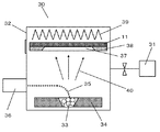
本実施の形態における膜厚測定方法と膜厚測定装置60は、PDP10の保護膜16を真空蒸着法によって形成する際に、インラインで膜厚を測定するのに用いる。図2は、保護膜16を形成するための真空蒸着装置30を示す図である。
The film thickness measuring method and the film
真空蒸着装置30は、真空ポンプ31が接続された真空チャンバー32内と、酸化マグネシウム(MgO)からなる保護膜原料33を保持するハース34と、保護膜原料33に電子ビーム35を照射する電子銃36とを備えている。また、真空チャンバー32の上部には、前面基板11を移載する開口部37が設けられたトレイ38と、前面基板11を所定温度まで加熱するヒータ39を備えられている。トレイ38には、誘電体層15が形成された前面基板11が誘電体層15の面が下面となるように載置されている。
The
このような真空蒸着装置30において、真空チャンバー32を酸素雰囲気の所定の真空度に維持し、電子ビーム35を保護膜原料33に照射することによって蒸発させ、蒸発粒子40が前面基板11の誘電体層15上に堆積して酸化マグネシウム(MgO)の保護膜16を製膜する。保護膜16が製膜された前面基板11を載せたトレイ38は、真空チャンバー32から排出され、次の前面基板11が載置されたトレイ38が再び真空蒸着装置30に移送されて製膜される。このような繰り返しをするプロセスの搬送途中で、真空蒸着後の保護膜16の膜厚をインラインで測定する。
In such a
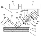
図3は、本実施の形態における膜厚測定装置60を示す図である。なお、インラインで膜厚を測定する際には、図3と上下が反転している。図3に示すように、被測定対象膜である保護膜16は、ガラス製の前面基板11上に形成された誘電体層15上に形成されている。
FIG. 3 is a diagram showing a film
図3に示すように、保護膜16の表面に対し45度以上の入射角度θでパルス光41を照射する光源42が設けられている。パルス光41によって、保護膜16の表面から反射した反射光、および保護膜16と基板となる誘電体層15との界面で反射した界面反射光とによって形成された干渉光43を分光器44で分光する。分光器44としては公知のグレーティングやプリズムを用いることができる。分光された干渉光45は、マルチアレイの光検出器46で検知される。すなわち、この膜厚測定装置60において、膜厚測定方法における光照射ステップと分光ステップと光検出ステップがなされる。
As shown in FIG. 3, a
近年、PDP10の発光効率の更なる向上が求められ、そのために、誘電体層15の比誘電率を小さくするようにしている。その結果、誘電体層15と、誘電体層15の上に形成される保護膜16との屈折率の差が非常に小さくなってきている。このため、非測定対象膜である保護膜16の膜厚を測定する際に、保護膜16と誘電体層15との界面での反射強度の差が弱まって干渉信号の強度が小さくなる。特に、従来のように光を保護膜16に垂直に照射する方式では、干渉信号の強度が小さくなり保護膜16の膜厚を精度良く測定できないという課題があった。
In recent years, further improvement in the light emission efficiency of the
そこで、本実施の形態では、パルス光41の入射角度を45度以上にすることで界面反射光の強度を大きくしている。そのため、保護膜16と誘電体層15との屈折率の差が小さくても保護膜16の膜厚を精度良く測定することができる。例えば、入射角を45度にすると反射率は1.4倍程度、60度にすることで界面での反射率は2倍程度にすることができる。
Therefore, in the present embodiment, the intensity of the interface reflected light is increased by setting the incident angle of the pulsed light 41 to 45 degrees or more. Therefore, even if the difference in refractive index between the
一方、従来の垂直入射の理由としては、光源と分光器、光検出器などが一体化できることや、基板搬送による振動によっても光の経路のずれが少なく、光検出器に入射する光束量が一定して安定な信号処理が行えるなどの利点があった。 On the other hand, the reason for conventional vertical incidence is that the light source, the spectroscope, the photodetector, etc. can be integrated, and there is little deviation of the light path due to vibration caused by substrate transport, and the amount of light incident on the photodetector is constant. Thus, there is an advantage that stable signal processing can be performed.
一方、上述のように入射角を大きくすることで界面反射率を上げることはできるが、真空蒸着装置30や基板搬送経路などからの反射光や散乱光によるノイズも多くなるので、干渉信号からこれを除去することが望ましい。そこで、本実施の形態では、光源42を電気的に、または、チョッパーなどを用いて機械的に点滅させて周期的なパルス光41としている。さらに、パルス光41の位相および周期と光検出器46からの出力とを、ロックインアンプなどの分離器47を用いて位相比較や検波し、パルス光41と異なる周期成分を除去することで外乱成分光を除去するようにしている。
On the other hand, although the interface reflectance can be increased by increasing the incident angle as described above, noise due to reflected light and scattered light from the
また、本実施の形態では、分光器44で分光した干渉光45を、光検出器46の前に置かれたビームスプリッター48で参照光49として分割するようにしている。参照光49は参照光検出器50で検知され、増倍機構51により増幅されて分離器47に入る。このような構成により、参照光49を用いて波長毎の光強度を補正して、干渉信号のピークを精度よく認識することができ、膜厚の測定精度をさらに高めることができる。なお、波長毎の光強度を補正する補正部は、本実施の形態では分離器47内に設けられ電気的に処理をされている。すなわち、この補正によって膜厚測定方法の補正ステップがなされる。
Further, in the present embodiment, the
また、分光器44には回動機構または移動機構を備えるようにしてもよい。すなわち、分光器44を僅かに回動または移動させることで、光検出器46に入射する光の波長を変化させることができ、これにより波長方向のデータ点数を増加させることができる。サンプリング定理によると、波長方向の測定点数が2倍になると、誤差は約1/2の平方根だけ小さくできる。そのため、干渉信号のピークをより精度よく検出することができ、膜厚の測定精度をさらに高めることができる。
The
また、本実施の形態では、光源42が近紫外光を含む光を照射し、光検出器46がこの近紫外光を検知可能としている。このように利用する波長領域に近紫外領域を含ませることで、膜厚としての測定精度を向上させることが可能になる。この理由について以下に述べる。
In the present embodiment, the
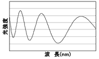
図4は、本発明の実施の形態における膜厚測定装置60における干渉信号の波長と光強度との関係を示す図である。図4に示すように、波長と光強度とは、信号強度が周期的に極大値、極小値を有し、波長が長くなるに従って強度が小さくなるとともに周期が大きくなることである。このことから短波長側の方が極値の数、即ちフリンジ数が増える。そのため、参照データを多くすることが可能となり、結果として、膜厚として換算する際の精度をさらに高めることができる。
FIG. 4 is a diagram showing the relationship between the wavelength of the interference signal and the light intensity in the film
また、この場合、分光器44も近紫外光に対応する必要がある。分光器44がグレーティングの場合には、分散を小さくして同じ出射角度に短波長が対応するようにするか、グレーティングの角度を変更することで対応することができる。一方、分光器44がプリズムの場合には、プリズムの屈折率をより大きくするか、プリズムの設置角度を変更することで対応することができる。
In this case, the
なお、参照データを多くするには、波長はできるだけ短波長側にシフトした方が望ましいが、大気中の透過率や、酸化マグネシウム(MgO)などの金属酸化物の透過率、光検出器46の特性などを考慮すると、350nm以上の近紫外域を使用することが望ましい。
In order to increase the reference data, it is desirable to shift the wavelength to the short wavelength side as much as possible. However, the transmittance in the atmosphere, the transmittance of a metal oxide such as magnesium oxide (MgO), the
また、本実施の形態では、光検出器46で取得した波長と光強度の関係を、波数と光強度の関係に換算した後にフーリエ変換などで周期情報に変換する変換部を備えている。周期情報としては、被測定対象膜である保護膜16を測定して得られる周期情報と、基板としての誘電体層15を測定して得られる周期情報との差分を算出するコンピュータなどの演算部52を備えている。また、変換部は演算部52内に設けられている。すなわち、この変換と演算によって膜厚測定方法の変換ステップと演算ステップがなされる。
In the present embodiment, a conversion unit that converts the relationship between the wavelength and the light intensity acquired by the
干渉信号は、保護膜16表面と、保護膜16と誘電体層15との界面での反射による干渉信号であるが、干渉信号としてはこの他に、誘電体層15と前面基板11としてのガラス基板の界面、ガラス基板の裏面、の計4箇所での反射の組合せとして計6通りの干渉信号の混じり合った状態で観測される。これらは全て、屈折率の厚み方向積分値(斜入射の場合には、その光路長での積分値)の整数倍で極大値を有し、それらの中間点で極小値を有する信号となる。そのため、干渉信号を波長と光強度の関係から、波長の逆数である波数と光強度との関係として求めると、等間隔に極大極小値を有することになる。
The interference signal is an interference signal due to reflection at the surface of the
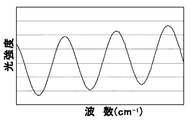
図5は、本発明の実施の形態における膜厚測定装置60における干渉信号の波数と光強度との関係を示す図である。ここで、波数と光強度との関係をフーリエ変換することによって周波数(ここでは次元は長さの次元になる)成分の分離を行うと、波数の間隔の逆数部分に大きな信号ピークが発生する。そのため、6通りの干渉信号でもそれぞれの波数の間隔の逆数部分にピークが発生し、それぞれの成分を分離することが可能となる。
FIG. 5 is a diagram showing the relationship between the wave number of the interference signal and the light intensity in the film
そこで、本実施の形態における膜厚測定方法および膜厚測定装置60では、まず、誘電体層15のみを形成して保護膜16を形成しない前面基板11を用いて測定を行い、演算部52により計3通りの組合せの干渉信号から周期成分を算出する。その後、保護膜16と誘電体層15を形成した前面基板11を用いて測定を行い、演算部52を用いて、計6通りの組合せの干渉信号から周期成分を算出する。これらの周期成分の差分を取ると、保護膜16が関与している3通りの干渉信号のみが残る。このうち、保護膜16の表面と、保護膜16と誘電体層15との界面での干渉信号は強度が最も高いので、残りの信号をノイズとして除去することができる。これにより保護膜16の膜厚の測定精度をより高めることができる。
Therefore, in the film thickness measuring method and film
このように、本実施の形態による膜厚測定装置60および膜厚測定方法を用い、PDP10の保護膜16を形成する際に、インラインでの高精度な保護膜16の膜厚測定が可能となる。特に、誘電体層15の材料として、保護膜16の材料とほぼ同じ屈折率を持つ程度まで比誘電率の低い材料を用いても、高精度な膜厚測定が実現でき、その結果を製膜プロセスに時間遅れがない状態でフィードバックすることができる。その結果、保護膜16の基板毎の膜厚ばらつきを抑制し、生産歩留まりを向上させることができる。
Thus, when forming the
なお、本実施の形態においては、酸化マグネシウム(MgO)からなるPDP10の保護膜16を測定する例を示したが、保護膜16の材料として、酸化アルミニウム(Al2O3)、酸化カルシウム(CaO)、酸化バリウム(BaO)、酸化チタン(TiO2)、酸化イットリウム(Y2O3)、酸化ランタン(La2O3)、酸化セリウム(CeO2)、酸化ハフニウム(HfO2)などの金属酸化物や混合酸化物で、耐イオン衝撃性に優れ、それによる二次電子放出係数の大きい材料からなる保護膜16も同様である。さらに、本発明の膜厚測定装置はPDPの保護膜に限らず、被測定対象膜との屈折率の差が小さい基板の上に形成された被測定対象膜の膜厚を、精度良くインラインで測定することが可能である。
In this embodiment, an example in which the
本発明による膜厚測定装置と膜厚測定方法によれば、非測定対象膜との屈折率の差が小さい基板の上に形成された被測定対象膜の膜厚を、精度良く測定することができ、表示デバイスやその他の電子デバイスなどの薄膜形成プロセスに有用である。 According to the film thickness measuring apparatus and the film thickness measuring method according to the present invention, it is possible to accurately measure the film thickness of the measurement target film formed on the substrate having a small difference in refractive index from the non-measurement target film. It is useful for thin film formation processes such as display devices and other electronic devices.
10 PDP
11 前面基板
12 走査電極
13 維持電極
14 表示電極対
15 誘電体層
16 保護膜
17 背面基板
18 データ電極
19 下地誘電体層
20 隔壁
21 ブラックストライプ
23 蛍光体層
30 真空蒸着装置
31 真空ポンプ
32 真空チャンバー
33 保護膜原料
34 ハース
35 電子ビーム
36 電子銃
37 開口部
38 トレイ
39 ヒータ
40 蒸発粒子
41 パルス光
42 光源
43 干渉光
44 分光器
45 干渉光
46 光検出器
47 分離器
48 ビームスプリッター
49 参照光
50 参照光検出器
51 増倍機構
52 演算部
60 膜厚測定装置
10 PDP
DESCRIPTION OF
Claims (8)
Priority Applications (1)
| Application Number | Priority Date | Filing Date | Title |
|---|---|---|---|
| JP2010110750A JP2011237355A (en) | 2010-05-13 | 2010-05-13 | Film thickness measuring method and film thickness measuring apparatus |
Applications Claiming Priority (1)
| Application Number | Priority Date | Filing Date | Title |
|---|---|---|---|
| JP2010110750A JP2011237355A (en) | 2010-05-13 | 2010-05-13 | Film thickness measuring method and film thickness measuring apparatus |
Publications (1)
| Publication Number | Publication Date |
|---|---|
| JP2011237355A true JP2011237355A (en) | 2011-11-24 |
Family
ID=45325491
Family Applications (1)
| Application Number | Title | Priority Date | Filing Date |
|---|---|---|---|
| JP2010110750A Pending JP2011237355A (en) | 2010-05-13 | 2010-05-13 | Film thickness measuring method and film thickness measuring apparatus |
Country Status (1)
| Country | Link |
|---|---|
| JP (1) | JP2011237355A (en) |
Cited By (3)
| Publication number | Priority date | Publication date | Assignee | Title |
|---|---|---|---|---|
| CN106104342A (en) * | 2014-03-18 | 2016-11-09 | 恩普乐股份有限公司 | Optical socket and optical module |
| CN107607051A (en) * | 2017-10-26 | 2018-01-19 | 京东方科技集团股份有限公司 | A kind of film thickness detecting device |
| JP2020016650A (en) * | 2018-07-17 | 2020-01-30 | 株式会社システムロード | Film thickness measurement method, and device of the same |
-
2010
- 2010-05-13 JP JP2010110750A patent/JP2011237355A/en active Pending
Cited By (4)
| Publication number | Priority date | Publication date | Assignee | Title |
|---|---|---|---|---|
| CN106104342A (en) * | 2014-03-18 | 2016-11-09 | 恩普乐股份有限公司 | Optical socket and optical module |
| CN106104342B (en) * | 2014-03-18 | 2018-07-17 | 恩普乐股份有限公司 | Optical receptacle and optical module |
| CN107607051A (en) * | 2017-10-26 | 2018-01-19 | 京东方科技集团股份有限公司 | A kind of film thickness detecting device |
| JP2020016650A (en) * | 2018-07-17 | 2020-01-30 | 株式会社システムロード | Film thickness measurement method, and device of the same |
Similar Documents
| Publication | Publication Date | Title |
|---|---|---|
| JP6490700B2 (en) | Optical filter and spectrometer | |
| CN103270575B (en) | Data collecting system and method for mass spectrography | |
| Van Hoek et al. | Artefact and distortion sources in time correlated single photon counting | |
| JP6210266B2 (en) | Camera and image processing method | |
| JP2011237355A (en) | Film thickness measuring method and film thickness measuring apparatus | |
| JP2010197358A (en) | Spectroscopic analysis device and element analysis device | |
| JP2972832B2 (en) | Electron spectrometer with spectrum shift correction function and spectrum shift correction method for electron spectrometry | |
| EP4135001B1 (en) | Photoelectric conversion device, electromagnetic wave detection device, photoelectric conversion method and electromagnetic wave detection method | |
| JP4199050B2 (en) | Quadrupole mass spectrometer and vacuum apparatus having the same | |
| US20220334016A1 (en) | Method for detecting pressure, and pressure sensor | |
| JP6672805B2 (en) | Tunable interference filter, electronic component, method for manufacturing electronic component, and electronic device | |
| JP5987393B2 (en) | Measuring method, measuring device, arithmetic circuit, measuring program | |
| KR101072941B1 (en) | Plasma display panel | |
| JP4747921B2 (en) | Defect inspection method for PDP substrate | |
| JP2007324077A (en) | Method for manufacturing plasma display panel | |
| JP2008304318A (en) | Method and system for manufacturing plasma display panel | |
| JP4631550B2 (en) | Plasma display panel, protective film, and plasma display panel inspection method | |
| US20200173845A1 (en) | Charge carrier multiplier structure | |
| JP4876665B2 (en) | Defect inspection method | |
| JP4852881B2 (en) | Plasma display panel inspection method | |
| WO2025004999A1 (en) | Data processing device, mass spectrometry system, and mass spectrometry data processing method | |
| RU2015124858A (en) | Gas electroluminescent ion detector and ion identification method | |
| Käfer et al. | Cherenkov detector prototype for ILC polarimetry | |
| JPS58158848A (en) | Electron detector | |
| JP2011081183A (en) | Method for manufacturing photomask and method for manufacturing plasma display panel |