JP2011237787A - 表示装置及び電子機器 - Google Patents
表示装置及び電子機器 Download PDFInfo
- Publication number
- JP2011237787A JP2011237787A JP2011088305A JP2011088305A JP2011237787A JP 2011237787 A JP2011237787 A JP 2011237787A JP 2011088305 A JP2011088305 A JP 2011088305A JP 2011088305 A JP2011088305 A JP 2011088305A JP 2011237787 A JP2011237787 A JP 2011237787A
- Authority
- JP
- Japan
- Prior art keywords
- signal lines
- signal
- transistor
- potential
- gate
- Prior art date
- Legal status (The legal status is an assumption and is not a legal conclusion. Google has not performed a legal analysis and makes no representation as to the accuracy of the status listed.)
- Granted
Links
- 230000006870 function Effects 0.000 claims abstract description 67
- 239000011159 matrix material Substances 0.000 claims abstract description 10
- 238000004891 communication Methods 0.000 claims description 7
- 239000010410 layer Substances 0.000 description 139
- 238000000034 method Methods 0.000 description 46
- 239000010408 film Substances 0.000 description 45
- 239000004065 semiconductor Substances 0.000 description 41
- 239000000758 substrate Substances 0.000 description 28
- 229910044991 metal oxide Inorganic materials 0.000 description 23
- 150000004706 metal oxides Chemical class 0.000 description 23
- 239000002245 particle Substances 0.000 description 19
- 239000012530 fluid Substances 0.000 description 16
- 239000000843 powder Substances 0.000 description 15
- 229910007541 Zn O Inorganic materials 0.000 description 13
- 229910052782 aluminium Inorganic materials 0.000 description 12
- 238000001962 electrophoresis Methods 0.000 description 11
- 239000011521 glass Substances 0.000 description 11
- XAGFODPZIPBFFR-UHFFFAOYSA-N aluminium Chemical compound [Al] XAGFODPZIPBFFR-UHFFFAOYSA-N 0.000 description 10
- 239000010936 titanium Substances 0.000 description 10
- 239000003990 capacitor Substances 0.000 description 9
- 238000007667 floating Methods 0.000 description 9
- 239000000463 material Substances 0.000 description 9
- 239000003094 microcapsule Substances 0.000 description 9
- 229910052581 Si3N4 Inorganic materials 0.000 description 8
- 230000001681 protective effect Effects 0.000 description 8
- HQVNEWCFYHHQES-UHFFFAOYSA-N silicon nitride Chemical compound N12[Si]34N5[Si]62N3[Si]51N64 HQVNEWCFYHHQES-UHFFFAOYSA-N 0.000 description 8
- 206010047571 Visual impairment Diseases 0.000 description 7
- 229910052750 molybdenum Inorganic materials 0.000 description 7
- VYPSYNLAJGMNEJ-UHFFFAOYSA-N silicon dioxide Inorganic materials O=[Si]=O VYPSYNLAJGMNEJ-UHFFFAOYSA-N 0.000 description 7
- XLOMVQKBTHCTTD-UHFFFAOYSA-N Zinc monoxide Chemical compound [Zn]=O XLOMVQKBTHCTTD-UHFFFAOYSA-N 0.000 description 6
- 229910021417 amorphous silicon Inorganic materials 0.000 description 6
- 239000004973 liquid crystal related substance Substances 0.000 description 6
- 239000011347 resin Substances 0.000 description 6
- 229920005989 resin Polymers 0.000 description 6
- 229910052710 silicon Inorganic materials 0.000 description 6
- 229910052814 silicon oxide Inorganic materials 0.000 description 6
- 229910052719 titanium Inorganic materials 0.000 description 6
- 229910052721 tungsten Inorganic materials 0.000 description 6
- XUIMIQQOPSSXEZ-UHFFFAOYSA-N Silicon Chemical compound [Si] XUIMIQQOPSSXEZ-UHFFFAOYSA-N 0.000 description 5
- 238000009825 accumulation Methods 0.000 description 5
- 239000000956 alloy Substances 0.000 description 5
- 229910052802 copper Inorganic materials 0.000 description 5
- 239000010949 copper Substances 0.000 description 5
- 230000005684 electric field Effects 0.000 description 5
- 229910052733 gallium Inorganic materials 0.000 description 5
- 239000012535 impurity Substances 0.000 description 5
- 239000007788 liquid Substances 0.000 description 5
- 238000012545 processing Methods 0.000 description 5
- 239000010703 silicon Substances 0.000 description 5
- 239000002904 solvent Substances 0.000 description 5
- 239000004986 Cholesteric liquid crystals (ChLC) Substances 0.000 description 4
- ZOKXTWBITQBERF-UHFFFAOYSA-N Molybdenum Chemical compound [Mo] ZOKXTWBITQBERF-UHFFFAOYSA-N 0.000 description 4
- 229910045601 alloy Inorganic materials 0.000 description 4
- 229910052804 chromium Inorganic materials 0.000 description 4
- 239000011651 chromium Substances 0.000 description 4
- 229910052751 metal Inorganic materials 0.000 description 4
- 239000011733 molybdenum Substances 0.000 description 4
- 238000007789 sealing Methods 0.000 description 4
- 239000002356 single layer Substances 0.000 description 4
- 229910052715 tantalum Inorganic materials 0.000 description 4
- RYGMFSIKBFXOCR-UHFFFAOYSA-N Copper Chemical compound [Cu] RYGMFSIKBFXOCR-UHFFFAOYSA-N 0.000 description 3
- 229910019092 Mg-O Inorganic materials 0.000 description 3
- 229910019395 Mg—O Inorganic materials 0.000 description 3
- RTAQQCXQSZGOHL-UHFFFAOYSA-N Titanium Chemical compound [Ti] RTAQQCXQSZGOHL-UHFFFAOYSA-N 0.000 description 3
- NRTOMJZYCJJWKI-UHFFFAOYSA-N Titanium nitride Chemical compound [Ti]#N NRTOMJZYCJJWKI-UHFFFAOYSA-N 0.000 description 3
- 239000000969 carrier Substances 0.000 description 3
- PMHQVHHXPFUNSP-UHFFFAOYSA-M copper(1+);methylsulfanylmethane;bromide Chemical compound Br[Cu].CSC PMHQVHHXPFUNSP-UHFFFAOYSA-M 0.000 description 3
- 238000010586 diagram Methods 0.000 description 3
- 238000004519 manufacturing process Methods 0.000 description 3
- 239000002184 metal Substances 0.000 description 3
- 229910021424 microcrystalline silicon Inorganic materials 0.000 description 3
- 230000003287 optical effect Effects 0.000 description 3
- 239000010937 tungsten Substances 0.000 description 3
- 239000011787 zinc oxide Substances 0.000 description 3
- 229910000838 Al alloy Inorganic materials 0.000 description 2
- 229910052779 Neodymium Inorganic materials 0.000 description 2
- 239000004983 Polymer Dispersed Liquid Crystal Substances 0.000 description 2
- 229910006404 SnO 2 Inorganic materials 0.000 description 2
- 239000000853 adhesive Substances 0.000 description 2
- 230000001070 adhesive effect Effects 0.000 description 2
- 239000012790 adhesive layer Substances 0.000 description 2
- 239000005407 aluminoborosilicate glass Substances 0.000 description 2
- 238000004458 analytical method Methods 0.000 description 2
- 229910052788 barium Inorganic materials 0.000 description 2
- DSAJWYNOEDNPEQ-UHFFFAOYSA-N barium atom Chemical compound [Ba] DSAJWYNOEDNPEQ-UHFFFAOYSA-N 0.000 description 2
- 230000015572 biosynthetic process Effects 0.000 description 2
- 239000005388 borosilicate glass Substances 0.000 description 2
- 239000003086 colorant Substances 0.000 description 2
- 230000007547 defect Effects 0.000 description 2
- 238000010438 heat treatment Methods 0.000 description 2
- 229910052739 hydrogen Inorganic materials 0.000 description 2
- 239000001257 hydrogen Substances 0.000 description 2
- 229910052738 indium Inorganic materials 0.000 description 2
- 239000012212 insulator Substances 0.000 description 2
- 229910052748 manganese Inorganic materials 0.000 description 2
- 239000011368 organic material Substances 0.000 description 2
- TWNQGVIAIRXVLR-UHFFFAOYSA-N oxo(oxoalumanyloxy)alumane Chemical compound O=[Al]O[Al]=O TWNQGVIAIRXVLR-UHFFFAOYSA-N 0.000 description 2
- 238000005192 partition Methods 0.000 description 2
- 239000000049 pigment Substances 0.000 description 2
- 229910052706 scandium Inorganic materials 0.000 description 2
- 238000004544 sputter deposition Methods 0.000 description 2
- 239000000126 substance Substances 0.000 description 2
- WFKWXMTUELFFGS-UHFFFAOYSA-N tungsten Chemical compound [W] WFKWXMTUELFFGS-UHFFFAOYSA-N 0.000 description 2
- 229910052725 zinc Inorganic materials 0.000 description 2
- 239000011701 zinc Substances 0.000 description 2
- HEZMWWAKWCSUCB-PHDIDXHHSA-N (3R,4R)-3,4-dihydroxycyclohexa-1,5-diene-1-carboxylic acid Chemical compound O[C@@H]1C=CC(C(O)=O)=C[C@H]1O HEZMWWAKWCSUCB-PHDIDXHHSA-N 0.000 description 1
- VYZAMTAEIAYCRO-UHFFFAOYSA-N Chromium Chemical compound [Cr] VYZAMTAEIAYCRO-UHFFFAOYSA-N 0.000 description 1
- 239000004593 Epoxy Substances 0.000 description 1
- UFHFLCQGNIYNRP-UHFFFAOYSA-N Hydrogen Chemical compound [H][H] UFHFLCQGNIYNRP-UHFFFAOYSA-N 0.000 description 1
- HBBGRARXTFLTSG-UHFFFAOYSA-N Lithium ion Chemical compound [Li+] HBBGRARXTFLTSG-UHFFFAOYSA-N 0.000 description 1
- OAICVXFJPJFONN-UHFFFAOYSA-N Phosphorus Chemical compound [P] OAICVXFJPJFONN-UHFFFAOYSA-N 0.000 description 1
- 239000004952 Polyamide Substances 0.000 description 1
- 239000004642 Polyimide Substances 0.000 description 1
- 229910000676 Si alloy Inorganic materials 0.000 description 1
- 229910004298 SiO 2 Inorganic materials 0.000 description 1
- 229910020923 Sn-O Inorganic materials 0.000 description 1
- 229910018725 Sn—Al Inorganic materials 0.000 description 1
- 229910052771 Terbium Inorganic materials 0.000 description 1
- 229910001069 Ti alloy Inorganic materials 0.000 description 1
- GDFCWFBWQUEQIJ-UHFFFAOYSA-N [B].[P] Chemical compound [B].[P] GDFCWFBWQUEQIJ-UHFFFAOYSA-N 0.000 description 1
- AZWHFTKIBIQKCA-UHFFFAOYSA-N [Sn+2]=O.[O-2].[In+3] Chemical compound [Sn+2]=O.[O-2].[In+3] AZWHFTKIBIQKCA-UHFFFAOYSA-N 0.000 description 1
- NIXOWILDQLNWCW-UHFFFAOYSA-N acrylic acid group Chemical group C(C=C)(=O)O NIXOWILDQLNWCW-UHFFFAOYSA-N 0.000 description 1
- 239000005354 aluminosilicate glass Substances 0.000 description 1
- QVQLCTNNEUAWMS-UHFFFAOYSA-N barium oxide Chemical compound [Ba]=O QVQLCTNNEUAWMS-UHFFFAOYSA-N 0.000 description 1
- UMIVXZPTRXBADB-UHFFFAOYSA-N benzocyclobutene Chemical compound C1=CC=C2CCC2=C1 UMIVXZPTRXBADB-UHFFFAOYSA-N 0.000 description 1
- 239000011230 binding agent Substances 0.000 description 1
- 239000005380 borophosphosilicate glass Substances 0.000 description 1
- 239000000919 ceramic Substances 0.000 description 1
- 238000006243 chemical reaction Methods 0.000 description 1
- 238000012790 confirmation Methods 0.000 description 1
- 238000007796 conventional method Methods 0.000 description 1
- 238000013461 design Methods 0.000 description 1
- 230000006866 deterioration Effects 0.000 description 1
- 238000011161 development Methods 0.000 description 1
- JKWMSGQKBLHBQQ-UHFFFAOYSA-N diboron trioxide Chemical compound O=BOB=O JKWMSGQKBLHBQQ-UHFFFAOYSA-N 0.000 description 1
- 238000009792 diffusion process Methods 0.000 description 1
- KPUWHANPEXNPJT-UHFFFAOYSA-N disiloxane Chemical class [SiH3]O[SiH3] KPUWHANPEXNPJT-UHFFFAOYSA-N 0.000 description 1
- 238000004070 electrodeposition Methods 0.000 description 1
- 230000007613 environmental effect Effects 0.000 description 1
- 230000005284 excitation Effects 0.000 description 1
- 239000007789 gas Substances 0.000 description 1
- 229910000449 hafnium oxide Inorganic materials 0.000 description 1
- WIHZLLGSGQNAGK-UHFFFAOYSA-N hafnium(4+);oxygen(2-) Chemical compound [O-2].[O-2].[Hf+4] WIHZLLGSGQNAGK-UHFFFAOYSA-N 0.000 description 1
- 150000002431 hydrogen Chemical class 0.000 description 1
- 229910003437 indium oxide Inorganic materials 0.000 description 1
- PJXISJQVUVHSOJ-UHFFFAOYSA-N indium(iii) oxide Chemical compound [O-2].[O-2].[O-2].[In+3].[In+3] PJXISJQVUVHSOJ-UHFFFAOYSA-N 0.000 description 1
- 238000001095 inductively coupled plasma mass spectrometry Methods 0.000 description 1
- 239000011261 inert gas Substances 0.000 description 1
- 229910001416 lithium ion Inorganic materials 0.000 description 1
- 230000014759 maintenance of location Effects 0.000 description 1
- 239000007769 metal material Substances 0.000 description 1
- 239000011859 microparticle Substances 0.000 description 1
- 239000000203 mixture Substances 0.000 description 1
- 229910021421 monocrystalline silicon Inorganic materials 0.000 description 1
- QEFYFXOXNSNQGX-UHFFFAOYSA-N neodymium atom Chemical compound [Nd] QEFYFXOXNSNQGX-UHFFFAOYSA-N 0.000 description 1
- 150000004767 nitrides Chemical class 0.000 description 1
- 229910052698 phosphorus Inorganic materials 0.000 description 1
- 239000011574 phosphorus Substances 0.000 description 1
- 238000005268 plasma chemical vapour deposition Methods 0.000 description 1
- 239000004033 plastic Substances 0.000 description 1
- 229920002647 polyamide Polymers 0.000 description 1
- 229910021420 polycrystalline silicon Inorganic materials 0.000 description 1
- 229920001721 polyimide Polymers 0.000 description 1
- 238000010248 power generation Methods 0.000 description 1
- 239000011241 protective layer Substances 0.000 description 1
- 239000010453 quartz Substances 0.000 description 1
- 229910052594 sapphire Inorganic materials 0.000 description 1
- 239000010980 sapphire Substances 0.000 description 1
- SIXSYDAISGFNSX-UHFFFAOYSA-N scandium atom Chemical compound [Sc] SIXSYDAISGFNSX-UHFFFAOYSA-N 0.000 description 1
- LIVNPJMFVYWSIS-UHFFFAOYSA-N silicon monoxide Chemical compound [Si-]#[O+] LIVNPJMFVYWSIS-UHFFFAOYSA-N 0.000 description 1
- 239000012798 spherical particle Substances 0.000 description 1
- GUVRBAGPIYLISA-UHFFFAOYSA-N tantalum atom Chemical compound [Ta] GUVRBAGPIYLISA-UHFFFAOYSA-N 0.000 description 1
- MZLGASXMSKOWSE-UHFFFAOYSA-N tantalum nitride Chemical compound [Ta]#N MZLGASXMSKOWSE-UHFFFAOYSA-N 0.000 description 1
- 239000010409 thin film Substances 0.000 description 1
- XOLBLPGZBRYERU-UHFFFAOYSA-N tin dioxide Chemical compound O=[Sn]=O XOLBLPGZBRYERU-UHFFFAOYSA-N 0.000 description 1
- 229910001887 tin oxide Inorganic materials 0.000 description 1
- -1 tungsten nitride Chemical class 0.000 description 1
- XLYOFNOQVPJJNP-UHFFFAOYSA-N water Substances O XLYOFNOQVPJJNP-UHFFFAOYSA-N 0.000 description 1
- 239000012463 white pigment Substances 0.000 description 1
- 238000003079 width control Methods 0.000 description 1
- 229910052727 yttrium Inorganic materials 0.000 description 1
- OYQCBJZGELKKPM-UHFFFAOYSA-N zinc indium(3+) oxygen(2-) Chemical compound [O-2].[Zn+2].[O-2].[In+3] OYQCBJZGELKKPM-UHFFFAOYSA-N 0.000 description 1
Images





Classifications
-
- G—PHYSICS
- G09—EDUCATION; CRYPTOGRAPHY; DISPLAY; ADVERTISING; SEALS
- G09G—ARRANGEMENTS OR CIRCUITS FOR CONTROL OF INDICATING DEVICES USING STATIC MEANS TO PRESENT VARIABLE INFORMATION
- G09G3/00—Control arrangements or circuits, of interest only in connection with visual indicators other than cathode-ray tubes
- G09G3/20—Control arrangements or circuits, of interest only in connection with visual indicators other than cathode-ray tubes for presentation of an assembly of a number of characters, e.g. a page, by composing the assembly by combination of individual elements arranged in a matrix no fixed position being assigned to or needed to be assigned to the individual characters or partial characters
- G09G3/34—Control arrangements or circuits, of interest only in connection with visual indicators other than cathode-ray tubes for presentation of an assembly of a number of characters, e.g. a page, by composing the assembly by combination of individual elements arranged in a matrix no fixed position being assigned to or needed to be assigned to the individual characters or partial characters by control of light from an independent source
- G09G3/3433—Control arrangements or circuits, of interest only in connection with visual indicators other than cathode-ray tubes for presentation of an assembly of a number of characters, e.g. a page, by composing the assembly by combination of individual elements arranged in a matrix no fixed position being assigned to or needed to be assigned to the individual characters or partial characters by control of light from an independent source using light modulating elements actuated by an electric field and being other than liquid crystal devices and electrochromic devices
- G09G3/344—Control arrangements or circuits, of interest only in connection with visual indicators other than cathode-ray tubes for presentation of an assembly of a number of characters, e.g. a page, by composing the assembly by combination of individual elements arranged in a matrix no fixed position being assigned to or needed to be assigned to the individual characters or partial characters by control of light from an independent source using light modulating elements actuated by an electric field and being other than liquid crystal devices and electrochromic devices based on particles moving in a fluid or in a gas, e.g. electrophoretic devices
-
- G—PHYSICS
- G09—EDUCATION; CRYPTOGRAPHY; DISPLAY; ADVERTISING; SEALS
- G09G—ARRANGEMENTS OR CIRCUITS FOR CONTROL OF INDICATING DEVICES USING STATIC MEANS TO PRESENT VARIABLE INFORMATION
- G09G2300/00—Aspects of the constitution of display devices
- G09G2300/08—Active matrix structure, i.e. with use of active elements, inclusive of non-linear two terminal elements, in the pixels together with light emitting or modulating elements
-
- G—PHYSICS
- G09—EDUCATION; CRYPTOGRAPHY; DISPLAY; ADVERTISING; SEALS
- G09G—ARRANGEMENTS OR CIRCUITS FOR CONTROL OF INDICATING DEVICES USING STATIC MEANS TO PRESENT VARIABLE INFORMATION
- G09G2310/00—Command of the display device
- G09G2310/02—Addressing, scanning or driving the display screen or processing steps related thereto
- G09G2310/0202—Addressing of scan or signal lines
- G09G2310/0205—Simultaneous scanning of several lines in flat panels
-
- G—PHYSICS
- G09—EDUCATION; CRYPTOGRAPHY; DISPLAY; ADVERTISING; SEALS
- G09G—ARRANGEMENTS OR CIRCUITS FOR CONTROL OF INDICATING DEVICES USING STATIC MEANS TO PRESENT VARIABLE INFORMATION
- G09G2310/00—Command of the display device
- G09G2310/02—Addressing, scanning or driving the display screen or processing steps related thereto
- G09G2310/0243—Details of the generation of driving signals
- G09G2310/0248—Precharge or discharge of column electrodes before or after applying exact column voltages
-
- G—PHYSICS
- G09—EDUCATION; CRYPTOGRAPHY; DISPLAY; ADVERTISING; SEALS
- G09G—ARRANGEMENTS OR CIRCUITS FOR CONTROL OF INDICATING DEVICES USING STATIC MEANS TO PRESENT VARIABLE INFORMATION
- G09G2310/00—Command of the display device
- G09G2310/02—Addressing, scanning or driving the display screen or processing steps related thereto
- G09G2310/0243—Details of the generation of driving signals
- G09G2310/0251—Precharge or discharge of pixel before applying new pixel voltage
-
- G—PHYSICS
- G09—EDUCATION; CRYPTOGRAPHY; DISPLAY; ADVERTISING; SEALS
- G09G—ARRANGEMENTS OR CIRCUITS FOR CONTROL OF INDICATING DEVICES USING STATIC MEANS TO PRESENT VARIABLE INFORMATION
- G09G2310/00—Command of the display device
- G09G2310/02—Addressing, scanning or driving the display screen or processing steps related thereto
- G09G2310/0264—Details of driving circuits
- G09G2310/0272—Details of drivers for data electrodes, the drivers communicating data to the pixels by means of a current
-
- G—PHYSICS
- G09—EDUCATION; CRYPTOGRAPHY; DISPLAY; ADVERTISING; SEALS
- G09G—ARRANGEMENTS OR CIRCUITS FOR CONTROL OF INDICATING DEVICES USING STATIC MEANS TO PRESENT VARIABLE INFORMATION
- G09G3/00—Control arrangements or circuits, of interest only in connection with visual indicators other than cathode-ray tubes
- G09G3/20—Control arrangements or circuits, of interest only in connection with visual indicators other than cathode-ray tubes for presentation of an assembly of a number of characters, e.g. a page, by composing the assembly by combination of individual elements arranged in a matrix no fixed position being assigned to or needed to be assigned to the individual characters or partial characters
- G09G3/34—Control arrangements or circuits, of interest only in connection with visual indicators other than cathode-ray tubes for presentation of an assembly of a number of characters, e.g. a page, by composing the assembly by combination of individual elements arranged in a matrix no fixed position being assigned to or needed to be assigned to the individual characters or partial characters by control of light from an independent source
- G09G3/3433—Control arrangements or circuits, of interest only in connection with visual indicators other than cathode-ray tubes for presentation of an assembly of a number of characters, e.g. a page, by composing the assembly by combination of individual elements arranged in a matrix no fixed position being assigned to or needed to be assigned to the individual characters or partial characters by control of light from an independent source using light modulating elements actuated by an electric field and being other than liquid crystal devices and electrochromic devices
Landscapes
- Engineering & Computer Science (AREA)
- Physics & Mathematics (AREA)
- Computer Hardware Design (AREA)
- General Physics & Mathematics (AREA)
- Theoretical Computer Science (AREA)
- Control Of Indicators Other Than Cathode Ray Tubes (AREA)
- Liquid Crystal Display Device Control (AREA)
- Liquid Crystal (AREA)
- Electrochromic Elements, Electrophoresis, Or Variable Reflection Or Absorption Elements (AREA)
Abstract
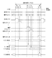
【解決手段】複数の画素、複数のゲート信号線、及び複数のソース信号線がマトリクス状に配置された表示部と、複数のゲート信号線のいずれか一を選択するタイミングを制御する機能を有する走査線駆動回路と、走査線駆動回路が複数のゲート信号線のいずれか一を選択する期間において、複数のソース信号線のすべてに第1の信号を出力した後、複数のソース信号線のいずれか一に第2の信号を出力するタイミングを制御する機能を有する信号線駆動回路と、を有し、複数の画素のそれぞれは、トランジスタと、画素電極とコモン電極とに挟持され、且つメモリ性を有する表示素子と、を有し、トランジスタの第1の端子は複数のソース信号線のいずれか一と電気的に接続され、トランジスタの第2の端子は画素電極と電気的に接続され、トランジスタのゲートは複数のゲート信号線のいずれか一と電気的に接続されるものである表示装置。
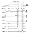
【選択図】図5
Description
本実施の形態では、開示する発明の一態様である表示装置及びその駆動方法について説明する。
本実施の形態では、実施の形態1とは異なる表示装置の駆動方法について説明する。本実施の形態では、実施の形態1と異なるところのみを説明し、実施の形態1と共通するところはその説明を省略する。
本実施の形態では、開示する発明の一態様である表示装置が有する信号線駆動回路の具体例及びその駆動方法について説明する。
本実施の形態では、実施の形態3とは異なる信号線駆動回路の具体例及びその駆動方法について説明する。本実施の形態では、実施の形態3と異なるところのみを説明し、実施の形態3と共通するところはその説明を省略する。
本実施の形態では、実施の形態3及び実施の形態4とは異なる信号線駆動回路の具体例及びその駆動方法について説明する。本実施の形態では、実施の形態4と異なるところのみを説明し、実施の形態4と共通するところはその説明を省略する。
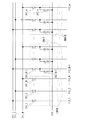
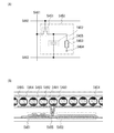
本実施の形態では、実施の形態3乃至実施の形態5において説明した信号線駆動回路が有するスイッチとして、トランジスタを用いた場合の例を説明する。
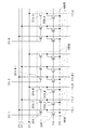
本実施の形態では、開示する発明の一態様である表示装置が有する画素の具体例及びその駆動方法について説明する。
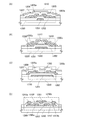
本実施の形態では、開示する発明の一態様である表示装置に用いることができるトランジスタの例について説明する。
本実施の形態では、上記実施の形態で示す表示装置において、タッチパネル機能を付加した表示装置の構成について、図20(A)、(B)を用いて説明する。
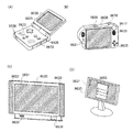
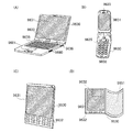
本実施の形態においては、上記実施の形態で説明した表示装置を具備する電子機器の例について説明する。
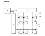
11 走査線駆動回路
12 信号線駆動回路
13 コントローラ
100 画素
111 ゲート信号線
112 ソース信号線
200 デマルチプレクサ回路
201 スイッチ
202 スイッチ
211 映像信号線
212 電源線
213 配線
214 配線
1200 基板
1201 ゲート電極層
1202 ゲート絶縁層
1203 半導体層
1207 絶縁層
1209 保護絶縁層
1210 トランジスタ
1220 トランジスタ
1227 絶縁層
1230 トランジスタ
1240 トランジスタ
1247 絶縁層
1501 表示パネル
1502 タッチパネルユニット
1503 筐体
1504 表示装置
1505 画素
1506 光センサ
1507 表示素子
1508 ゲート線側駆動回路
1509 信号線側駆動回路
1510 光センサ用駆動回路
201A トランジスタ
202A トランジスタ
5450 画素
5451 トランジスタ
5452 容量素子
5453 表示素子
5454 コモン電極
5455 画素電極
5461 ソース信号線
5462 ゲート信号線
5463 配線
5480 マイクロカプセル
5481 樹脂
5482 膜
5483 液体
5484 粒子
5485 粒子
5486 ツイストボール
5487 粒子
5488 キャビティ
5491 マイクロカップ
5492 誘電性溶媒
5493 帯電色素粒子
5494 封止層
5495 粘着層
5501 隔壁
5502 粉流体
5503 粉流体
9630 筐体
9631 表示部
9632 操作キー
9633 スピーカ
9635 操作キー
9636 接続端子
9638 マイクロフォン
9651 太陽電池
9652 バッテリー
9653 ウインドウ型表示部
9672 記録媒体読込部
9676 シャッターボタン
9677 受像部
9680 外部接続ポート
9681 ポインティングデバイス
1205a ソース電極層
1205b ドレイン電極層
1246a 配線層
1246b 配線層
Claims (7)
- 複数の画素、複数のゲート信号線、及び複数のソース信号線がマトリクス状に配置された表示部と、
前記複数のゲート信号線のいずれか一を選択するタイミングを制御する機能を有する走査線駆動回路と、
前記走査線駆動回路が前記複数のゲート信号線のいずれか一を選択する期間において、前記複数のソース信号線のすべてに第1の信号を出力した後、前記複数のソース信号線のいずれか一に第2の信号を出力するタイミングを制御する機能を有する信号線駆動回路と、を有し、
前記複数の画素のそれぞれは、トランジスタと、画素電極とコモン電極とに挟持され、且つメモリ性を有する表示素子と、を有し、
前記トランジスタの第1の端子は前記複数のソース信号線のいずれか一と電気的に接続され、前記トランジスタの第2の端子は前記画素電極と電気的に接続され、前記トランジスタのゲートは前記複数のゲート信号線のいずれか一と電気的に接続されるものである表示装置。 - 複数の画素、複数のゲート信号線、及びN(Nは自然数)個の群に分割される複数のソース信号線がマトリクス状に配置された表示部と、
前記複数のゲート信号線のいずれか一を選択するタイミングを制御する機能を有する走査線駆動回路と、
前記走査線駆動回路が前記複数のゲート信号線のいずれか一を選択する期間において、前記N個の群のすべてのソース信号線に第1の信号を出力した後、前記N個の群のソース信号線に、1群ずつ順番に第2の信号を出力するタイミングを制御する機能を有する信号線駆動回路と、を有し、
前記複数の画素のそれぞれは、トランジスタと、画素電極とコモン電極とに挟持され、且つメモリ性を有する表示素子と、を有し、
前記トランジスタの第1の端子は前記複数のソース信号線のいずれか一と電気的に接続され、前記トランジスタの第2の端子は前記画素電極と電気的に接続され、前記トランジスタのゲートは前記複数のゲート信号線のいずれか一と電気的に接続されるものである表示装置。 - 複数の画素、複数のゲート信号線、及びN(Nは自然数)個の群に分割される複数のソース信号線がマトリクス状に配置された表示部と、
前記複数のゲート信号線のいずれか一を選択するタイミングを制御する機能を有する走査線駆動回路と、
前記走査線駆動回路が前記複数のゲート信号線のいずれか一を選択する期間において、前記2個目乃至N個目のソース信号線に第1の信号を出力し、且つ前記1個目のソース信号線に第2の信号を出力した後、前記2個目乃至N個目の群のソース信号線に、1群ずつ順番に前記第2の信号を出力するタイミングを制御する機能を有する信号線駆動回路と、を有し、
前記複数の画素のそれぞれは、トランジスタと、画素電極とコモン電極とに挟持され、且つメモリ性を有する表示素子と、を有し、
前記トランジスタの第1の端子は前記複数のソース信号線のいずれか一と電気的に接続され、前記トランジスタの第2の端子は前記画素電極と電気的に接続され、前記トランジスタのゲートは前記複数のゲート信号線のいずれか一と電気的に接続されるものである表示装置。 - 請求項1乃至請求項3のいずれか一項において、
前記第1の信号の電位は、前記コモン電極の電位と等しいものである表示装置。 - 請求項1乃至請求項3のいずれか一項において、
前記第1の信号の電位と前記コモン電極の電位との電位差の絶対値は、前記表示素子の閾値電圧の絶対値よりも小さいものである表示装置。 - 請求項1乃至請求項5のいずれか一項において、
前記第2の信号は、前記コモン電極の電位とおおむね等しい値と、前記コモン電極の電位よりも高い値と、前記コモン電極の電位よりも低い値との3値を有するものである表示装置。 - 請求項1乃至請求項4のいずれか一項の表示装置と、通信機能とを有する電子機器。
Priority Applications (1)
| Application Number | Priority Date | Filing Date | Title |
|---|---|---|---|
| JP2011088305A JP5780811B2 (ja) | 2010-04-14 | 2011-04-12 | 表示装置及び電子機器 |
Applications Claiming Priority (3)
| Application Number | Priority Date | Filing Date | Title |
|---|---|---|---|
| JP2010093394 | 2010-04-14 | ||
| JP2010093394 | 2010-04-14 | ||
| JP2011088305A JP5780811B2 (ja) | 2010-04-14 | 2011-04-12 | 表示装置及び電子機器 |
Related Child Applications (1)
| Application Number | Title | Priority Date | Filing Date |
|---|---|---|---|
| JP2015140482A Division JP6043410B2 (ja) | 2010-04-14 | 2015-07-14 | 表示装置及び電子機器 |
Publications (2)
| Publication Number | Publication Date |
|---|---|
| JP2011237787A true JP2011237787A (ja) | 2011-11-24 |
| JP5780811B2 JP5780811B2 (ja) | 2015-09-16 |
Family
ID=44787877
Family Applications (2)
| Application Number | Title | Priority Date | Filing Date |
|---|---|---|---|
| JP2011088305A Expired - Fee Related JP5780811B2 (ja) | 2010-04-14 | 2011-04-12 | 表示装置及び電子機器 |
| JP2015140482A Expired - Fee Related JP6043410B2 (ja) | 2010-04-14 | 2015-07-14 | 表示装置及び電子機器 |
Family Applications After (1)
| Application Number | Title | Priority Date | Filing Date |
|---|---|---|---|
| JP2015140482A Expired - Fee Related JP6043410B2 (ja) | 2010-04-14 | 2015-07-14 | 表示装置及び電子機器 |
Country Status (4)
| Country | Link |
|---|---|
| US (1) | US9251741B2 (ja) |
| JP (2) | JP5780811B2 (ja) |
| KR (1) | KR101823319B1 (ja) |
| TW (1) | TWI529681B (ja) |
Cited By (3)
| Publication number | Priority date | Publication date | Assignee | Title |
|---|---|---|---|---|
| WO2018143025A1 (ja) * | 2017-01-31 | 2018-08-09 | シャープ株式会社 | 表示装置およびその駆動方法 |
| JP2019174596A (ja) * | 2018-03-28 | 2019-10-10 | シャープ株式会社 | アクティブマトリクス基板および表示装置 |
| JP2019174595A (ja) * | 2018-03-28 | 2019-10-10 | シャープ株式会社 | アクティブマトリクス基板および表示装置 |
Families Citing this family (6)
| Publication number | Priority date | Publication date | Assignee | Title |
|---|---|---|---|---|
| JP3117704B2 (ja) | 1990-11-02 | 2000-12-18 | 株式会社小松製作所 | 流動層を用いた冷却処理方法 |
| CN102750901A (zh) * | 2012-07-05 | 2012-10-24 | 深圳市华星光电技术有限公司 | 显示装置的驱动方法 |
| FR2998989B1 (fr) * | 2012-12-05 | 2015-01-02 | Thales Sa | Dispositif tactile multitouches a detection capacitive multifrequence et barycentrique |
| CN110010086B (zh) * | 2019-03-29 | 2020-12-22 | 上海中航光电子有限公司 | 电润湿面板的驱动方法 |
| KR102639309B1 (ko) * | 2019-06-12 | 2024-02-23 | 삼성디스플레이 주식회사 | 표시 장치 |
| CN118871855A (zh) * | 2023-02-28 | 2024-10-29 | 京东方科技集团股份有限公司 | 显示装置及驱动方法 |
Citations (9)
| Publication number | Priority date | Publication date | Assignee | Title |
|---|---|---|---|---|
| JPH02204718A (ja) * | 1989-02-02 | 1990-08-14 | Sony Corp | 液晶ディスプレイ装置 |
| JPH1152931A (ja) * | 1997-06-04 | 1999-02-26 | Sharp Corp | アクティブマトリクス型画像表示装置 |
| JPH11160730A (ja) * | 1997-11-27 | 1999-06-18 | Seiko Epson Corp | 液晶装置及び電子機器 |
| JP2004102055A (ja) * | 2002-09-11 | 2004-04-02 | Seiko Epson Corp | 分散系駆動回路の駆動方法、分散系駆動回路、電気泳動表示装置の駆動方法、電気泳動表示装置及び電子機器 |
| JP2008046485A (ja) * | 2006-08-18 | 2008-02-28 | Nec Electronics Corp | 表示装置、表示パネルの駆動装置、及び表示装置の駆動方法 |
| JP2008145556A (ja) * | 2006-12-07 | 2008-06-26 | Seiko Epson Corp | 電気光学装置、駆動方法および電子機器 |
| JP2009116247A (ja) * | 2007-11-09 | 2009-05-28 | Seiko Epson Corp | 駆動装置及び方法、並びに電気光学装置及び電子機器 |
| JP2009122157A (ja) * | 2007-11-12 | 2009-06-04 | Seiko Epson Corp | 駆動装置及び方法、並びに電気光学装置及び電子機器 |
| JP2009163246A (ja) * | 2008-01-04 | 2009-07-23 | Sony United Kingdom Ltd | 液晶ディスプレイ用駆動回路 |
Family Cites Families (15)
| Publication number | Priority date | Publication date | Assignee | Title |
|---|---|---|---|---|
| JP3837948B2 (ja) | 1999-01-29 | 2006-10-25 | セイコーエプソン株式会社 | 電気泳動インク表示装置 |
| EP1724750B1 (en) | 1999-01-29 | 2008-08-27 | Seiko Epson Corporation | Electrophoretic ink display apparatus using a piezoelectric transducer |
| GB0130017D0 (en) * | 2001-12-15 | 2002-02-06 | Koninkl Philips Electronics Nv | Active matrix liquid crystal display devices |
| KR100649243B1 (ko) * | 2002-03-21 | 2006-11-24 | 삼성에스디아이 주식회사 | 유기 전계발광 표시 장치 및 그 구동 방법 |
| JP4517576B2 (ja) * | 2002-12-10 | 2010-08-04 | セイコーエプソン株式会社 | 電気光学装置 |
| CN1784709A (zh) | 2003-05-05 | 2006-06-07 | 皇家飞利浦电子股份有限公司 | 电泳显示设备 |
| JP4105132B2 (ja) * | 2003-08-22 | 2008-06-25 | シャープ株式会社 | 表示装置の駆動回路、表示装置および表示装置の駆動方法 |
| TWI232426B (en) * | 2004-04-08 | 2005-05-11 | Toppoly Optoelectronics Corp | Circuitry and method for displaying of a monitor |
| JP2006091845A (ja) * | 2004-08-27 | 2006-04-06 | Seiko Epson Corp | 電気光学装置用駆動回路及びその駆動方法、並びに電気光学装置及び電子機器 |
| JP4367386B2 (ja) * | 2004-10-25 | 2009-11-18 | セイコーエプソン株式会社 | 電気光学装置、その駆動回路、駆動方法および電子機器 |
| JP4744851B2 (ja) * | 2004-11-12 | 2011-08-10 | ルネサスエレクトロニクス株式会社 | 駆動回路及び表示装置 |
| JP4529139B2 (ja) | 2005-08-31 | 2010-08-25 | セイコーエプソン株式会社 | 電気泳動装置の駆動方法、電気泳動装置を制御するためのコントローラ、電気泳動装置、および電子機器 |
| TWI380114B (en) * | 2005-12-15 | 2012-12-21 | Nlt Technologies Ltd | Electrophoretic display device and driving method for same |
| KR101361996B1 (ko) | 2006-12-23 | 2014-02-12 | 엘지디스플레이 주식회사 | 전기영동 표시장치와 그 구동방법 |
| KR20100038920A (ko) | 2008-10-07 | 2010-04-15 | 엘지디스플레이 주식회사 | 전기 영동 표시장치 |
-
2011
- 2011-04-11 US US13/084,030 patent/US9251741B2/en not_active Expired - Fee Related
- 2011-04-11 TW TW100112458A patent/TWI529681B/zh not_active IP Right Cessation
- 2011-04-12 KR KR1020110033630A patent/KR101823319B1/ko not_active Expired - Fee Related
- 2011-04-12 JP JP2011088305A patent/JP5780811B2/ja not_active Expired - Fee Related
-
2015
- 2015-07-14 JP JP2015140482A patent/JP6043410B2/ja not_active Expired - Fee Related
Patent Citations (9)
| Publication number | Priority date | Publication date | Assignee | Title |
|---|---|---|---|---|
| JPH02204718A (ja) * | 1989-02-02 | 1990-08-14 | Sony Corp | 液晶ディスプレイ装置 |
| JPH1152931A (ja) * | 1997-06-04 | 1999-02-26 | Sharp Corp | アクティブマトリクス型画像表示装置 |
| JPH11160730A (ja) * | 1997-11-27 | 1999-06-18 | Seiko Epson Corp | 液晶装置及び電子機器 |
| JP2004102055A (ja) * | 2002-09-11 | 2004-04-02 | Seiko Epson Corp | 分散系駆動回路の駆動方法、分散系駆動回路、電気泳動表示装置の駆動方法、電気泳動表示装置及び電子機器 |
| JP2008046485A (ja) * | 2006-08-18 | 2008-02-28 | Nec Electronics Corp | 表示装置、表示パネルの駆動装置、及び表示装置の駆動方法 |
| JP2008145556A (ja) * | 2006-12-07 | 2008-06-26 | Seiko Epson Corp | 電気光学装置、駆動方法および電子機器 |
| JP2009116247A (ja) * | 2007-11-09 | 2009-05-28 | Seiko Epson Corp | 駆動装置及び方法、並びに電気光学装置及び電子機器 |
| JP2009122157A (ja) * | 2007-11-12 | 2009-06-04 | Seiko Epson Corp | 駆動装置及び方法、並びに電気光学装置及び電子機器 |
| JP2009163246A (ja) * | 2008-01-04 | 2009-07-23 | Sony United Kingdom Ltd | 液晶ディスプレイ用駆動回路 |
Cited By (5)
| Publication number | Priority date | Publication date | Assignee | Title |
|---|---|---|---|---|
| WO2018143025A1 (ja) * | 2017-01-31 | 2018-08-09 | シャープ株式会社 | 表示装置およびその駆動方法 |
| JP2019174596A (ja) * | 2018-03-28 | 2019-10-10 | シャープ株式会社 | アクティブマトリクス基板および表示装置 |
| JP2019174595A (ja) * | 2018-03-28 | 2019-10-10 | シャープ株式会社 | アクティブマトリクス基板および表示装置 |
| CN110320688A (zh) * | 2018-03-28 | 2019-10-11 | 夏普株式会社 | 有源矩阵基板和显示装置 |
| US10896656B2 (en) | 2018-03-28 | 2021-01-19 | Sharp Kabushiki Kaisha | Active matrix substrate and display device including demultiplexer circuit with reduced drive power |
Also Published As
| Publication number | Publication date |
|---|---|
| TWI529681B (zh) | 2016-04-11 |
| JP2016014880A (ja) | 2016-01-28 |
| JP5780811B2 (ja) | 2015-09-16 |
| TW201211976A (en) | 2012-03-16 |
| US9251741B2 (en) | 2016-02-02 |
| JP6043410B2 (ja) | 2016-12-14 |
| KR101823319B1 (ko) | 2018-01-31 |
| KR20110115086A (ko) | 2011-10-20 |
| US20110254816A1 (en) | 2011-10-20 |
Similar Documents
| Publication | Publication Date | Title |
|---|---|---|
| JP6043410B2 (ja) | 表示装置及び電子機器 | |
| JP5809442B2 (ja) | 表示装置 | |
| JP7516497B2 (ja) | 表示装置 | |
| JP6362733B2 (ja) | 表示装置の駆動方法 | |
| CN102844873B (zh) | 半导体显示装置 | |
| JP2021113973A (ja) | 表示装置 | |
| WO2011099376A1 (en) | Liquid crystal display device and electronic device | |
| US20090128723A1 (en) | Liquid crystal display device | |
| JP2026074010A (ja) | 半導体装置 |
Legal Events
| Date | Code | Title | Description |
|---|---|---|---|
| A621 | Written request for application examination |
Free format text: JAPANESE INTERMEDIATE CODE: A621 Effective date: 20140331 |
|
| A977 | Report on retrieval |
Free format text: JAPANESE INTERMEDIATE CODE: A971007 Effective date: 20141128 |
|
| A131 | Notification of reasons for refusal |
Free format text: JAPANESE INTERMEDIATE CODE: A131 Effective date: 20141202 |
|
| A521 | Request for written amendment filed |
Free format text: JAPANESE INTERMEDIATE CODE: A523 Effective date: 20141208 |
|
| A131 | Notification of reasons for refusal |
Free format text: JAPANESE INTERMEDIATE CODE: A131 Effective date: 20150224 |
|
| A521 | Request for written amendment filed |
Free format text: JAPANESE INTERMEDIATE CODE: A523 Effective date: 20150303 |
|
| A131 | Notification of reasons for refusal |
Free format text: JAPANESE INTERMEDIATE CODE: A131 Effective date: 20150519 |
|
| A521 | Request for written amendment filed |
Free format text: JAPANESE INTERMEDIATE CODE: A523 Effective date: 20150528 |
|
| TRDD | Decision of grant or rejection written | ||
| A01 | Written decision to grant a patent or to grant a registration (utility model) |
Free format text: JAPANESE INTERMEDIATE CODE: A01 Effective date: 20150630 |
|
| A61 | First payment of annual fees (during grant procedure) |
Free format text: JAPANESE INTERMEDIATE CODE: A61 Effective date: 20150714 |
|
| R150 | Certificate of patent or registration of utility model |
Ref document number: 5780811 Country of ref document: JP Free format text: JAPANESE INTERMEDIATE CODE: R150 |
|
| R250 | Receipt of annual fees |
Free format text: JAPANESE INTERMEDIATE CODE: R250 |
|
| R250 | Receipt of annual fees |
Free format text: JAPANESE INTERMEDIATE CODE: R250 |
|
| R250 | Receipt of annual fees |
Free format text: JAPANESE INTERMEDIATE CODE: R250 |
|
| LAPS | Cancellation because of no payment of annual fees |