JP2012015209A - 貫通配線基板および製造方法 - Google Patents
貫通配線基板および製造方法 Download PDFInfo
- Publication number
- JP2012015209A JP2012015209A JP2010148197A JP2010148197A JP2012015209A JP 2012015209 A JP2012015209 A JP 2012015209A JP 2010148197 A JP2010148197 A JP 2010148197A JP 2010148197 A JP2010148197 A JP 2010148197A JP 2012015209 A JP2012015209 A JP 2012015209A
- Authority
- JP
- Japan
- Prior art keywords
- resin
- substrate
- manufacturing
- curing
- hole
- Prior art date
- Legal status (The legal status is an assumption and is not a legal conclusion. Google has not performed a legal analysis and makes no representation as to the accuracy of the status listed.)
- Granted
Links
- 238000004519 manufacturing process Methods 0.000 title claims abstract description 26
- 239000000758 substrate Substances 0.000 claims abstract description 104
- 239000011347 resin Substances 0.000 claims abstract description 95
- 229920005989 resin Polymers 0.000 claims abstract description 95
- 239000004020 conductor Substances 0.000 claims abstract description 33
- 229920001721 polyimide Polymers 0.000 claims abstract description 16
- 239000004642 Polyimide Substances 0.000 claims abstract description 9
- 239000007787 solid Substances 0.000 claims abstract description 6
- 229920000642 polymer Polymers 0.000 claims abstract description 5
- 239000011521 glass Substances 0.000 claims abstract description 4
- 238000010438 heat treatment Methods 0.000 claims description 29
- 239000000463 material Substances 0.000 claims description 29
- 238000001723 curing Methods 0.000 claims description 14
- 238000000034 method Methods 0.000 claims description 11
- 230000008018 melting Effects 0.000 claims description 5
- 238000002844 melting Methods 0.000 claims description 5
- 238000000016 photochemical curing Methods 0.000 claims description 5
- 230000035515 penetration Effects 0.000 claims description 4
- 206010034972 Photosensitivity reaction Diseases 0.000 claims description 3
- 238000005530 etching Methods 0.000 claims description 3
- 230000001678 irradiating effect Effects 0.000 claims description 3
- 230000036211 photosensitivity Effects 0.000 claims description 3
- 238000005498 polishing Methods 0.000 claims description 3
- 238000003780 insertion Methods 0.000 claims 2
- 230000037431 insertion Effects 0.000 claims 2
- 239000011800 void material Substances 0.000 abstract description 5
- 230000015572 biosynthetic process Effects 0.000 abstract description 4
- 229910052751 metal Inorganic materials 0.000 description 8
- 239000002184 metal Substances 0.000 description 8
- 238000005219 brazing Methods 0.000 description 7
- CSCPPACGZOOCGX-UHFFFAOYSA-N Acetone Chemical compound CC(C)=O CSCPPACGZOOCGX-UHFFFAOYSA-N 0.000 description 4
- 238000001312 dry etching Methods 0.000 description 4
- 230000004048 modification Effects 0.000 description 4
- 238000012986 modification Methods 0.000 description 4
- 239000000155 melt Substances 0.000 description 3
- 239000009719 polyimide resin Substances 0.000 description 3
- 238000007789 sealing Methods 0.000 description 3
- 239000002904 solvent Substances 0.000 description 3
- 238000001039 wet etching Methods 0.000 description 3
- PXHVJJICTQNCMI-UHFFFAOYSA-N Nickel Chemical compound [Ni] PXHVJJICTQNCMI-UHFFFAOYSA-N 0.000 description 2
- 238000007872 degassing Methods 0.000 description 2
- 229910000833 kovar Inorganic materials 0.000 description 2
- 229920005575 poly(amic acid) Polymers 0.000 description 2
- 229910000640 Fe alloy Inorganic materials 0.000 description 1
- ZOKXTWBITQBERF-UHFFFAOYSA-N Molybdenum Chemical compound [Mo] ZOKXTWBITQBERF-UHFFFAOYSA-N 0.000 description 1
- 239000004820 Pressure-sensitive adhesive Substances 0.000 description 1
- 239000000853 adhesive Substances 0.000 description 1
- 230000001070 adhesive effect Effects 0.000 description 1
- 239000004840 adhesive resin Substances 0.000 description 1
- 229920006223 adhesive resin Polymers 0.000 description 1
- 239000005388 borosilicate glass Substances 0.000 description 1
- 239000000919 ceramic Substances 0.000 description 1
- 229910017052 cobalt Inorganic materials 0.000 description 1
- 239000010941 cobalt Substances 0.000 description 1
- GUTLYIVDDKVIGB-UHFFFAOYSA-N cobalt atom Chemical compound [Co] GUTLYIVDDKVIGB-UHFFFAOYSA-N 0.000 description 1
- 230000006866 deterioration Effects 0.000 description 1
- 230000002542 deteriorative effect Effects 0.000 description 1
- 238000001035 drying Methods 0.000 description 1
- 230000005684 electric field Effects 0.000 description 1
- 238000001704 evaporation Methods 0.000 description 1
- 230000008020 evaporation Effects 0.000 description 1
- 238000010884 ion-beam technique Methods 0.000 description 1
- UGKDIUIOSMUOAW-UHFFFAOYSA-N iron nickel Chemical compound [Fe].[Ni] UGKDIUIOSMUOAW-UHFFFAOYSA-N 0.000 description 1
- 229910052750 molybdenum Inorganic materials 0.000 description 1
- 239000011733 molybdenum Substances 0.000 description 1
- 229910052759 nickel Inorganic materials 0.000 description 1
- 239000004065 semiconductor Substances 0.000 description 1
- 238000000926 separation method Methods 0.000 description 1
- 229910052710 silicon Inorganic materials 0.000 description 1
- 239000010703 silicon Substances 0.000 description 1
- 239000007921 spray Substances 0.000 description 1
- 239000010935 stainless steel Substances 0.000 description 1
- 229910001220 stainless steel Inorganic materials 0.000 description 1
- WFKWXMTUELFFGS-UHFFFAOYSA-N tungsten Chemical compound [W] WFKWXMTUELFFGS-UHFFFAOYSA-N 0.000 description 1
- 229910052721 tungsten Inorganic materials 0.000 description 1
- 239000010937 tungsten Substances 0.000 description 1
Images


Landscapes
- Printing Elements For Providing Electric Connections Between Printed Circuits (AREA)
- Internal Circuitry In Semiconductor Integrated Circuit Devices (AREA)
Abstract
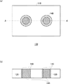
【解決手段】貫通ビアが設けられた貫通配線基板であって、貫通孔が形成された基板と、貫通孔内に設けられ、基板の上面と下面の間を電気的に接続する導電体と、導電体と貫通孔の間の隙間に充填された樹脂と、を備える貫通配線基板および製造方法を提供する。基板は、ガラス基板であってよい。樹脂は、ポリイミドであってよい。樹脂は、ポリマーであってもよい。樹脂は、光に反応して固体に変化する光硬化樹脂であってもよい。
【選択図】図1
Description
特許文献1 特開2006−60119号公報
Claims (19)
- 貫通ビアが設けられた貫通配線基板であって、
貫通孔が形成された基板と、
前期貫通孔内に設けられ、前記基板の上面と下面の間を電気的に接続する導電体と、
前記導電体と前記貫通孔の間の隙間に充填された樹脂と、
を備える貫通配線基板。 - 前記基板は、ガラス基板である請求項1に記載の貫通配線基板。
- 前記樹脂は、ポリイミドである請求項1または2に記載の貫通配線基板。
- 前記樹脂は、ポリマーである請求項1または2に記載の貫通配線基板。
- 前記樹脂は、光に反応して固体に変化する光硬化樹脂である請求項1または2に記載の貫通配線基板。
- 貫通ビアが設けられた貫通配線基板を製造する製造方法であって、
基板に貫通孔を形成する形成段階と、
前記貫通孔が開けられた前期基板に支持基盤を張り合わせ、前記貫通孔内に導電体を挿入する挿入段階と、
前記基板の前記支持基盤を張り合わせた面と反対側の面に樹脂を塗布して、前記導電体と前記貫通孔の間の隙間に前記樹脂を充填する充填段階と、
前記樹脂を硬化させる硬化段階と、
前記基板の表面の前記樹脂を除去する除去段階と、
を備える貫通配線基板を製造する製造方法。 - 前記基板は、ガラス基板である請求項6に記載の製造方法。
- 前記樹脂は、ポリイミドである請求項6または7に記載の製造方法。
- 前記樹脂は、ポリマーである請求項6または7に記載の製造方法。
- 前記充填段階は、前記樹脂を少なくとも2回に分けて充填し、先に充填する前記樹脂は、後に充填する前記樹脂よりも粘性の高い請求項6から9のいずれかに記載の製造方法。
- 前記樹脂は、光に反応して固体に変化する光硬化樹脂であり、
前記硬化段階は、前記基板に光を照射して前記樹脂を硬化させる請求項6または7に記載の製造方法。 - 前記硬化段階は、前記樹脂を熱処理によって硬化させる、請求項6から10のいずれかに記載の製造方法。
- 前記充填段階は、前記基板と前記支持基盤とを張り合わせ材によって張り合わせ、
前記硬化段階は、前記樹脂を複数回の熱処理によって硬化させ、
前記張り合わせ材は、前記硬化段階の少なくとも1回の熱処理によって融解して、前記基板と前記支持基盤とを分離する請求項6から10のいずれかに記載の製造方法。 - 前記張り合わせ材を融解させる熱処理の温度は、前記樹脂を硬化させる熱処理の温度とは異なる請求項12に記載の製造方法。
- 前記充填段階は、前記基板と前記支持基盤とを張り合わせ材によって張り合わせ、
前記硬化段階は、前記張り合わせ材を剥離液によって融解し、前記基板と前記支持基盤とを分離する請求項6から11のいずれかに記載の製造方法。 - 前記挿入段階は、前記基板上にレジストを塗布して固化されたレジストを前記支持基盤とし、
前記硬化段階は、前記レジストを現像液または剥離液によって前記基板と分離する請求項6から12のいずれかに記載の製造方法。 - 前記除去段階は、前記硬化段階において前記基板の表面で硬化した前記樹脂を研磨によって除去する請求項6から16のいずれかに記載の製造方法。
- 前記除去段階は、前記硬化段階において前記基板の表面で硬化した前記樹脂をエッチングによって除去する請求項6から16のいずれかに記載の製造方法。
- 前記樹脂は感光性を有し、
前記除去段階は、前記基板の表面に塗布された前記樹脂にマスクを介して光を照射して、現像液で前記樹脂の露光部分を除去し、
前記硬化段階は、前記除去段階において除去されなかった前記樹脂を硬化する請求項6から16のいずれかに記載の製造方法。
Priority Applications (1)
| Application Number | Priority Date | Filing Date | Title |
|---|---|---|---|
| JP2010148197A JP5547566B2 (ja) | 2010-06-29 | 2010-06-29 | 貫通配線基板の製造方法 |
Applications Claiming Priority (1)
| Application Number | Priority Date | Filing Date | Title |
|---|---|---|---|
| JP2010148197A JP5547566B2 (ja) | 2010-06-29 | 2010-06-29 | 貫通配線基板の製造方法 |
Publications (2)
| Publication Number | Publication Date |
|---|---|
| JP2012015209A true JP2012015209A (ja) | 2012-01-19 |
| JP5547566B2 JP5547566B2 (ja) | 2014-07-16 |
Family
ID=45601322
Family Applications (1)
| Application Number | Title | Priority Date | Filing Date |
|---|---|---|---|
| JP2010148197A Expired - Fee Related JP5547566B2 (ja) | 2010-06-29 | 2010-06-29 | 貫通配線基板の製造方法 |
Country Status (1)
| Country | Link |
|---|---|
| JP (1) | JP5547566B2 (ja) |
Cited By (7)
| Publication number | Priority date | Publication date | Assignee | Title |
|---|---|---|---|---|
| WO2015147785A1 (en) * | 2014-03-24 | 2015-10-01 | Intel Corporation | Through-body via formation techniques |
| WO2016035625A1 (ja) * | 2014-09-03 | 2016-03-10 | 国立大学法人東北大学 | 半導体装置およびその製造方法 |
| WO2016114133A1 (ja) * | 2015-01-15 | 2016-07-21 | 凸版印刷株式会社 | インターポーザ、半導体装置、およびそれらの製造方法 |
| WO2017164043A1 (ja) * | 2016-03-25 | 2017-09-28 | 住友精密工業株式会社 | 充填方法 |
| JP2018190752A (ja) * | 2017-04-28 | 2018-11-29 | 日本シイエムケイ株式会社 | プリント配線板の製造方法 |
| WO2019065656A1 (ja) * | 2017-09-29 | 2019-04-04 | 大日本印刷株式会社 | 貫通電極基板及び貫通電極基板を用いた半導体装置 |
| CN109688699A (zh) * | 2018-12-31 | 2019-04-26 | 深圳硅基仿生科技有限公司 | 陶瓷电路板及其制造方法 |
Citations (4)
| Publication number | Priority date | Publication date | Assignee | Title |
|---|---|---|---|---|
| JP2003046226A (ja) * | 2001-07-30 | 2003-02-14 | Kyocera Corp | 配線基板およびその製造方法 |
| JP2003115658A (ja) * | 2001-10-05 | 2003-04-18 | Advantest Corp | 配線基板の製造方法、充填物挿入方法、配線基板、及び素子パッケージ |
| JP2008300782A (ja) * | 2007-06-04 | 2008-12-11 | Shinko Electric Ind Co Ltd | 貫通電極付き基板の製造方法 |
| JP2009105326A (ja) * | 2007-10-25 | 2009-05-14 | Shinko Electric Ind Co Ltd | 貫通電極付き基板の製造方法 |
-
2010
- 2010-06-29 JP JP2010148197A patent/JP5547566B2/ja not_active Expired - Fee Related
Patent Citations (4)
| Publication number | Priority date | Publication date | Assignee | Title |
|---|---|---|---|---|
| JP2003046226A (ja) * | 2001-07-30 | 2003-02-14 | Kyocera Corp | 配線基板およびその製造方法 |
| JP2003115658A (ja) * | 2001-10-05 | 2003-04-18 | Advantest Corp | 配線基板の製造方法、充填物挿入方法、配線基板、及び素子パッケージ |
| JP2008300782A (ja) * | 2007-06-04 | 2008-12-11 | Shinko Electric Ind Co Ltd | 貫通電極付き基板の製造方法 |
| JP2009105326A (ja) * | 2007-10-25 | 2009-05-14 | Shinko Electric Ind Co Ltd | 貫通電極付き基板の製造方法 |
Cited By (14)
| Publication number | Priority date | Publication date | Assignee | Title |
|---|---|---|---|---|
| WO2015147785A1 (en) * | 2014-03-24 | 2015-10-01 | Intel Corporation | Through-body via formation techniques |
| US9852964B2 (en) | 2014-03-24 | 2017-12-26 | Intel Corporation | Through-body via formation techniques |
| JPWO2016035625A1 (ja) * | 2014-09-03 | 2017-06-15 | 国立大学法人東北大学 | 半導体装置およびその製造方法 |
| CN107078055A (zh) * | 2014-09-03 | 2017-08-18 | 国立大学法人东北大学 | 半导体装置及其制造方法 |
| WO2016035625A1 (ja) * | 2014-09-03 | 2016-03-10 | 国立大学法人東北大学 | 半導体装置およびその製造方法 |
| US10177118B2 (en) | 2014-09-03 | 2019-01-08 | Tohoku University | Semiconductor device and method for manufacturing the same |
| US10483240B2 (en) | 2014-09-03 | 2019-11-19 | Tohoku University | Semiconductor device and method for manufacturing the same |
| WO2016114133A1 (ja) * | 2015-01-15 | 2016-07-21 | 凸版印刷株式会社 | インターポーザ、半導体装置、およびそれらの製造方法 |
| WO2017164043A1 (ja) * | 2016-03-25 | 2017-09-28 | 住友精密工業株式会社 | 充填方法 |
| JPWO2017164043A1 (ja) * | 2016-03-25 | 2018-10-18 | 住友精密工業株式会社 | 充填方法 |
| JP2018190752A (ja) * | 2017-04-28 | 2018-11-29 | 日本シイエムケイ株式会社 | プリント配線板の製造方法 |
| WO2019065656A1 (ja) * | 2017-09-29 | 2019-04-04 | 大日本印刷株式会社 | 貫通電極基板及び貫通電極基板を用いた半導体装置 |
| JPWO2019065656A1 (ja) * | 2017-09-29 | 2020-11-19 | 大日本印刷株式会社 | 貫通電極基板及び貫通電極基板を用いた半導体装置 |
| CN109688699A (zh) * | 2018-12-31 | 2019-04-26 | 深圳硅基仿生科技有限公司 | 陶瓷电路板及其制造方法 |
Also Published As
| Publication number | Publication date |
|---|---|
| JP5547566B2 (ja) | 2014-07-16 |
Similar Documents
| Publication | Publication Date | Title |
|---|---|---|
| JP5547566B2 (ja) | 貫通配線基板の製造方法 | |
| US8334174B2 (en) | Chip scale package and fabrication method thereof | |
| JP2009530801A (ja) | 回路基板の製造方法とコンポーネントを有する回路基板 | |
| US20170245365A1 (en) | Printed wiring board and method for manufacturing the same | |
| US8327532B2 (en) | Method for releasing a microelectronic assembly from a carrier substrate | |
| JP3501360B2 (ja) | ポリマ補強カラム・グリッド・アレイ | |
| CN101515592A (zh) | 基板模块、基板模块的制造方法及电子机器 | |
| JP6201610B2 (ja) | 電子装置の製造方法及び回路基板 | |
| US4635346A (en) | Method for producing hybrid integrated circuit | |
| CN104081521A (zh) | 用于在封装期间应用芯片支撑来生产重组晶片的方法 | |
| JP6116476B2 (ja) | チップスタックを製造するための方法及びその方法を実施するためのキャリア | |
| JP2011187913A (ja) | 電子素子内蔵型印刷回路基板及びその製造方法 | |
| JP5485818B2 (ja) | 貫通配線基板および製造方法 | |
| JP2019019153A (ja) | 接着材料及び回路基板の製造方法 | |
| JP2018041827A (ja) | 部品内蔵基板及び電子装置 | |
| TWI904961B (zh) | 同時巨量轉移微導電柱的方法及設備 | |
| US20140301050A1 (en) | Substrate assembly, method of manufacturing substrate assembly and method of manufacturing chip package | |
| CN205944063U (zh) | 封装基板 | |
| TWI883533B (zh) | 電路基板結構及其製造方法 | |
| CN205609508U (zh) | 叠层封装体组件以及封装体叠层组件 | |
| CN101231961B (zh) | 内埋组件的基板制程 | |
| JPS5848947A (ja) | 半導体装置の製法 | |
| JP2002313994A (ja) | 回路基板の製造方法 | |
| JP2011054852A (ja) | 半導体装置の製造方法 | |
| CN116525458A (zh) | 用于嵌入式芯片的封装制程 |
Legal Events
| Date | Code | Title | Description |
|---|---|---|---|
| A621 | Written request for application examination |
Free format text: JAPANESE INTERMEDIATE CODE: A621 Effective date: 20120830 |
|
| A131 | Notification of reasons for refusal |
Free format text: JAPANESE INTERMEDIATE CODE: A131 Effective date: 20130611 |
|
| A977 | Report on retrieval |
Free format text: JAPANESE INTERMEDIATE CODE: A971007 Effective date: 20130613 |
|
| A521 | Written amendment |
Free format text: JAPANESE INTERMEDIATE CODE: A523 Effective date: 20130801 |
|
| A131 | Notification of reasons for refusal |
Free format text: JAPANESE INTERMEDIATE CODE: A131 Effective date: 20140218 |
|
| A521 | Written amendment |
Free format text: JAPANESE INTERMEDIATE CODE: A523 Effective date: 20140328 |
|
| TRDD | Decision of grant or rejection written | ||
| A01 | Written decision to grant a patent or to grant a registration (utility model) |
Free format text: JAPANESE INTERMEDIATE CODE: A01 Effective date: 20140507 |
|
| A61 | First payment of annual fees (during grant procedure) |
Free format text: JAPANESE INTERMEDIATE CODE: A61 Effective date: 20140515 |
|
| R150 | Certificate of patent or registration of utility model |
Ref document number: 5547566 Country of ref document: JP Free format text: JAPANESE INTERMEDIATE CODE: R150 |
|
| LAPS | Cancellation because of no payment of annual fees |