JP2012015334A - 配線基板およびその製造方法 - Google Patents
配線基板およびその製造方法 Download PDFInfo
- Publication number
- JP2012015334A JP2012015334A JP2010150479A JP2010150479A JP2012015334A JP 2012015334 A JP2012015334 A JP 2012015334A JP 2010150479 A JP2010150479 A JP 2010150479A JP 2010150479 A JP2010150479 A JP 2010150479A JP 2012015334 A JP2012015334 A JP 2012015334A
- Authority
- JP
- Japan
- Prior art keywords
- layer
- plating layer
- electroless plating
- wiring conductor
- main surface
- Prior art date
- Legal status (The legal status is an assumption and is not a legal conclusion. Google has not performed a legal analysis and makes no representation as to the accuracy of the status listed.)
- Granted
Links
- 238000004519 manufacturing process Methods 0.000 title description 62
- 239000004020 conductor Substances 0.000 claims abstract description 90
- 238000007772 electroless plating Methods 0.000 claims abstract description 75
- 239000011888 foil Substances 0.000 claims abstract description 73
- 229910052751 metal Inorganic materials 0.000 claims abstract description 73
- 239000002184 metal Substances 0.000 claims abstract description 73
- 239000004065 semiconductor Substances 0.000 claims abstract description 47
- 238000000034 method Methods 0.000 claims abstract description 34
- 239000000654 additive Substances 0.000 claims abstract description 21
- 239000010410 layer Substances 0.000 claims description 255
- 239000000758 substrate Substances 0.000 claims description 70
- 229920005989 resin Polymers 0.000 claims description 46
- 239000011347 resin Substances 0.000 claims description 46
- 238000009713 electroplating Methods 0.000 claims description 41
- 238000005530 etching Methods 0.000 claims description 29
- RYGMFSIKBFXOCR-UHFFFAOYSA-N Copper Chemical compound [Cu] RYGMFSIKBFXOCR-UHFFFAOYSA-N 0.000 claims description 23
- 239000011889 copper foil Substances 0.000 claims description 13
- 239000004744 fabric Substances 0.000 claims description 11
- 239000011521 glass Substances 0.000 claims description 11
- 238000000151 deposition Methods 0.000 claims description 5
- 239000002356 single layer Substances 0.000 claims description 4
- 238000009413 insulation Methods 0.000 abstract 4
- 238000007747 plating Methods 0.000 description 25
- 229910052802 copper Inorganic materials 0.000 description 10
- 239000010949 copper Substances 0.000 description 10
- 229920001187 thermosetting polymer Polymers 0.000 description 9
- 239000003822 epoxy resin Substances 0.000 description 5
- 229920000647 polyepoxide Polymers 0.000 description 5
- 229910000679 solder Inorganic materials 0.000 description 5
- JYEUMXHLPRZUAT-UHFFFAOYSA-N 1,2,3-triazine Chemical compound C1=CN=NN=C1 JYEUMXHLPRZUAT-UHFFFAOYSA-N 0.000 description 4
- XQUPVDVFXZDTLT-UHFFFAOYSA-N 1-[4-[[4-(2,5-dioxopyrrol-1-yl)phenyl]methyl]phenyl]pyrrole-2,5-dione Chemical compound O=C1C=CC(=O)N1C(C=C1)=CC=C1CC1=CC=C(N2C(C=CC2=O)=O)C=C1 XQUPVDVFXZDTLT-UHFFFAOYSA-N 0.000 description 4
- 229920003192 poly(bis maleimide) Polymers 0.000 description 4
- 239000012777 electrically insulating material Substances 0.000 description 3
- 238000010030 laminating Methods 0.000 description 3
- 238000007788 roughening Methods 0.000 description 3
- 239000012286 potassium permanganate Substances 0.000 description 2
- 206010034972 Photosensitivity reaction Diseases 0.000 description 1
- 230000015572 biosynthetic process Effects 0.000 description 1
- 238000005868 electrolysis reaction Methods 0.000 description 1
- 239000011810 insulating material Substances 0.000 description 1
- 239000007788 liquid Substances 0.000 description 1
- 239000000463 material Substances 0.000 description 1
- 238000012986 modification Methods 0.000 description 1
- 230000004048 modification Effects 0.000 description 1
- 230000036211 photosensitivity Effects 0.000 description 1
- 238000003825 pressing Methods 0.000 description 1
- 230000003746 surface roughness Effects 0.000 description 1
Images


Landscapes
- Production Of Multi-Layered Print Wiring Board (AREA)
- Manufacturing Of Printed Wiring (AREA)
Abstract
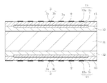
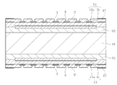
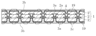
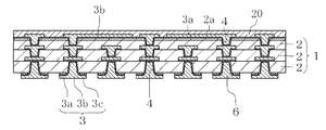
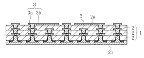
【解決手段】絶縁基板1の一方の主面に半導体素子接続パッド5を含む第1の配線導体3がセミアディティブ法により被着形成されているとともに絶縁基板1の他方の主面に外部接続パッド6を含む第2の配線導体3がセミアディティブ法により被着形成されて成る配線基板であって、第1の配線導体3は一方の主面の絶縁層2上に被着された無電解めっき層3aおよびその上の電解めっき層3bから成り、第2の配線導体3は、他方の主面の絶縁層2上に直接被着された金属箔3cおよびその無電解めっき層3aおよびその上の電解めっき層3bから成る。
【選択図】図1
Description
2 絶縁層
2a 樹脂層
3 配線導体
5 半導体素子接続パッド
6 外部接続パッド
10 積層体
11 支持基板
Claims (3)
- ガラスクロス入りのプリプレグを硬化させて成る単層または多層の絶縁層を含む絶縁基板の一方の主面に半導体素子の電極に接続される半導体素子接続パッドを含む第1の配線導体がセミアディティブ法により被着形成されているとともに前記絶縁基板の他方の主面に外部電気回路基板に接続される外部接続パッドを含む第2の配線導体がセミアディティブ法により被着形成されて成る配線基板であって、前記第1の配線導体は前記一方の主面の絶縁層上に被着された無電解めっき層および該無電解めっき層上の電解めっき層から成り、前記第2の配線導体は、前記他方の主面の絶縁層上に直接被着された銅箔および該銅箔上の無電解めっき層および該無電解めっき層上の電解めっき層から成ることを特徴とする配線基板。
- 前記第1の配線導体は、前記絶縁層上に樹脂層を介して被着されており、前記第2の配線導体は、前記絶縁層上に直接被着されていることを特徴とする請求項1記載の配線基板。
- ガラスクロス入りのプリプレグを硬化させて成る単層または多層の絶縁層を含む絶縁基板の一方の主面に第1の金属箔が前記絶縁層上に直接または樹脂層を介して被着されているとともに前記絶縁基板の他方の主面に第2の金属箔が前記絶縁層上に直接被着されて成る積層体を準備する工程と、前記第1の金属箔をエッチングして前記一方の主面の絶縁層またはその上の樹脂層を露出させる工程と、前記一方の主面の絶縁層またはその上の樹脂層表面および前記第2の金属箔の表面に無電解めっき層を被着させる工程と、前記一方の主面側の無電解めっき層上に半導体素子の電極に接続される半導体素子接続パッドを含む第1の配線導体に対応するパターンの電解めっき層を被着させるとともに前記他方の主面側の無電解めっき層上に外部電気回路基板に接続される外部接続パッドを含む第2の配線導体に対応するパターンの電解めっき層を被着させる工程と、前記電解めっき層から露出する前記無電解めっき層および前記第2の金属箔をエッチング除去することにより前記一方の主面の絶縁層上に直接または樹脂層を介して被着された無電解めっき層および該無電解めっき層上の電解めっき層から成る前記第1の配線導体を形成するとともに前記他方の主面の絶縁層上に直接被着され第2の金属箔および該第2の金属箔上の無電解めっき層および該無電解めっき層上の電解めっき層から成る前記第2の配線導体を形成する工程とを行なうことを特徴とする配線基板の製造方法。
Priority Applications (1)
| Application Number | Priority Date | Filing Date | Title |
|---|---|---|---|
| JP2010150479A JP5557320B2 (ja) | 2010-06-30 | 2010-06-30 | 配線基板の製造方法 |
Applications Claiming Priority (1)
| Application Number | Priority Date | Filing Date | Title |
|---|---|---|---|
| JP2010150479A JP5557320B2 (ja) | 2010-06-30 | 2010-06-30 | 配線基板の製造方法 |
Publications (2)
| Publication Number | Publication Date |
|---|---|
| JP2012015334A true JP2012015334A (ja) | 2012-01-19 |
| JP5557320B2 JP5557320B2 (ja) | 2014-07-23 |
Family
ID=45601403
Family Applications (1)
| Application Number | Title | Priority Date | Filing Date |
|---|---|---|---|
| JP2010150479A Active JP5557320B2 (ja) | 2010-06-30 | 2010-06-30 | 配線基板の製造方法 |
Country Status (1)
| Country | Link |
|---|---|
| JP (1) | JP5557320B2 (ja) |
Cited By (2)
| Publication number | Priority date | Publication date | Assignee | Title |
|---|---|---|---|---|
| WO2014109357A1 (ja) * | 2013-01-09 | 2014-07-17 | 日立化成株式会社 | 配線基板の製造方法及び支持材付き積層体 |
| JP2016134395A (ja) * | 2015-01-15 | 2016-07-25 | イビデン株式会社 | プリント配線板の製造方法 |
Citations (5)
| Publication number | Priority date | Publication date | Assignee | Title |
|---|---|---|---|---|
| JP2004158521A (ja) * | 2002-11-05 | 2004-06-03 | Nec Toppan Circuit Solutions Inc | 多層印刷配線板及びその製造方法並びに半導体装置 |
| WO2007052674A1 (ja) * | 2005-11-02 | 2007-05-10 | Ibiden Co., Ltd. | 半導体装置用多層プリント配線板及びその製造方法 |
| JP2007173459A (ja) * | 2005-12-21 | 2007-07-05 | Ibiden Co Ltd | プリント配線板の製造方法 |
| JP2007188986A (ja) * | 2006-01-12 | 2007-07-26 | Tdk Corp | 多層回路基板及びその製造方法 |
| JP2009206409A (ja) * | 2008-02-29 | 2009-09-10 | Kyocer Slc Technologies Corp | 配線基板の製造方法 |
-
2010
- 2010-06-30 JP JP2010150479A patent/JP5557320B2/ja active Active
Patent Citations (5)
| Publication number | Priority date | Publication date | Assignee | Title |
|---|---|---|---|---|
| JP2004158521A (ja) * | 2002-11-05 | 2004-06-03 | Nec Toppan Circuit Solutions Inc | 多層印刷配線板及びその製造方法並びに半導体装置 |
| WO2007052674A1 (ja) * | 2005-11-02 | 2007-05-10 | Ibiden Co., Ltd. | 半導体装置用多層プリント配線板及びその製造方法 |
| JP2007173459A (ja) * | 2005-12-21 | 2007-07-05 | Ibiden Co Ltd | プリント配線板の製造方法 |
| JP2007188986A (ja) * | 2006-01-12 | 2007-07-26 | Tdk Corp | 多層回路基板及びその製造方法 |
| JP2009206409A (ja) * | 2008-02-29 | 2009-09-10 | Kyocer Slc Technologies Corp | 配線基板の製造方法 |
Cited By (2)
| Publication number | Priority date | Publication date | Assignee | Title |
|---|---|---|---|---|
| WO2014109357A1 (ja) * | 2013-01-09 | 2014-07-17 | 日立化成株式会社 | 配線基板の製造方法及び支持材付き積層体 |
| JP2016134395A (ja) * | 2015-01-15 | 2016-07-25 | イビデン株式会社 | プリント配線板の製造方法 |
Also Published As
| Publication number | Publication date |
|---|---|
| JP5557320B2 (ja) | 2014-07-23 |
Similar Documents
| Publication | Publication Date | Title |
|---|---|---|
| US9756735B2 (en) | Method for manufacturing printed wiring board | |
| US10745819B2 (en) | Printed wiring board, semiconductor package and method for manufacturing printed wiring board | |
| US20180033732A1 (en) | Wiring board | |
| JP4994988B2 (ja) | 配線基板の製造方法 | |
| JP4691763B2 (ja) | プリント配線板の製造方法 | |
| KR20120040892A (ko) | 인쇄회로기판 및 그의 제조 방법 | |
| US20130160290A1 (en) | Method of manufacturing multi-layer wiring board | |
| JP6084283B2 (ja) | 部品内蔵基板及びその製造方法 | |
| JP5047906B2 (ja) | 配線基板の製造方法 | |
| JP5177855B2 (ja) | 配線基板の製造方法 | |
| JP5557320B2 (ja) | 配線基板の製造方法 | |
| JP2011139010A (ja) | 回路基板およびその製造方法 | |
| JP2020057767A (ja) | プリント配線基板 | |
| JP2004207338A (ja) | 配線基板 | |
| JPWO2014188493A1 (ja) | 部品内蔵基板及びその製造方法 | |
| JP2002185139A (ja) | プリント配線板及びその製造方法 | |
| JP4742409B2 (ja) | プリント配線板の製造方法 | |
| JP2009194312A (ja) | 配線基板およびその製造方法 | |
| JP5409519B2 (ja) | 配線基板およびその製造方法 | |
| JP2004241427A (ja) | 配線基板の製造方法 | |
| JP2012099586A (ja) | 配線基板およびその製造方法 | |
| JP2012209322A (ja) | 配線基板の製造方法 | |
| JP4492071B2 (ja) | 配線基板の製造方法 | |
| JP2015144152A (ja) | 配線基板の製造方法 | |
| JP2002185134A (ja) | プリント配線板及びその製造方法 |
Legal Events
| Date | Code | Title | Description |
|---|---|---|---|
| A621 | Written request for application examination |
Free format text: JAPANESE INTERMEDIATE CODE: A621 Effective date: 20130206 |
|
| A977 | Report on retrieval |
Free format text: JAPANESE INTERMEDIATE CODE: A971007 Effective date: 20131114 |
|
| A131 | Notification of reasons for refusal |
Free format text: JAPANESE INTERMEDIATE CODE: A131 Effective date: 20131118 |
|
| A521 | Written amendment |
Free format text: JAPANESE INTERMEDIATE CODE: A523 Effective date: 20140116 |
|
| A02 | Decision of refusal |
Free format text: JAPANESE INTERMEDIATE CODE: A02 Effective date: 20140205 |
|
| A521 | Written amendment |
Free format text: JAPANESE INTERMEDIATE CODE: A523 Effective date: 20140411 |
|
| A911 | Transfer of reconsideration by examiner before appeal (zenchi) |
Free format text: JAPANESE INTERMEDIATE CODE: A911 Effective date: 20140422 |
|
| TRDD | Decision of grant or rejection written | ||
| A01 | Written decision to grant a patent or to grant a registration (utility model) |
Free format text: JAPANESE INTERMEDIATE CODE: A01 Effective date: 20140528 |
|
| A61 | First payment of annual fees (during grant procedure) |
Free format text: JAPANESE INTERMEDIATE CODE: A61 Effective date: 20140530 |
|
| R150 | Certificate of patent or registration of utility model |
Ref document number: 5557320 Country of ref document: JP Free format text: JAPANESE INTERMEDIATE CODE: R150 |
|
| S531 | Written request for registration of change of domicile |
Free format text: JAPANESE INTERMEDIATE CODE: R313531 |
|
| S533 | Written request for registration of change of name |
Free format text: JAPANESE INTERMEDIATE CODE: R313533 |
|
| R350 | Written notification of registration of transfer |
Free format text: JAPANESE INTERMEDIATE CODE: R350 |
|
| S111 | Request for change of ownership or part of ownership |
Free format text: JAPANESE INTERMEDIATE CODE: R313111 |
|
| R350 | Written notification of registration of transfer |
Free format text: JAPANESE INTERMEDIATE CODE: R350 |