JP2012019247A - 部品内蔵基板の製造方法 - Google Patents
部品内蔵基板の製造方法 Download PDFInfo
- Publication number
- JP2012019247A JP2012019247A JP2011234623A JP2011234623A JP2012019247A JP 2012019247 A JP2012019247 A JP 2012019247A JP 2011234623 A JP2011234623 A JP 2011234623A JP 2011234623 A JP2011234623 A JP 2011234623A JP 2012019247 A JP2012019247 A JP 2012019247A
- Authority
- JP
- Japan
- Prior art keywords
- component
- chip component
- insulator
- substrate
- electrode
- Prior art date
- Legal status (The legal status is an assumption and is not a legal conclusion. Google has not performed a legal analysis and makes no representation as to the accuracy of the status listed.)
- Pending
Links
Images


Classifications
-
- H—ELECTRICITY
- H05—ELECTRIC TECHNIQUES NOT OTHERWISE PROVIDED FOR
- H05K—PRINTED CIRCUITS; CASINGS OR CONSTRUCTIONAL DETAILS OF ELECTRIC APPARATUS; MANUFACTURE OF ASSEMBLAGES OF ELECTRICAL COMPONENTS
- H05K1/00—Printed circuits
- H05K1/18—Printed circuits structurally associated with non-printed electric components
- H05K1/182—Printed circuits structurally associated with non-printed electric components associated with components mounted in printed circuit boards [PCB], e.g. insert-mounted components [IMC]
- H05K1/185—Printed circuits structurally associated with non-printed electric components associated with components mounted in printed circuit boards [PCB], e.g. insert-mounted components [IMC] associated with components encapsulated in the insulating substrate of the PCBs; associated with components incorporated in internal layers of multilayer circuit boards
-
- H—ELECTRICITY
- H05—ELECTRIC TECHNIQUES NOT OTHERWISE PROVIDED FOR
- H05K—PRINTED CIRCUITS; CASINGS OR CONSTRUCTIONAL DETAILS OF ELECTRIC APPARATUS; MANUFACTURE OF ASSEMBLAGES OF ELECTRICAL COMPONENTS
- H05K2201/00—Indexing scheme relating to printed circuits covered by H05K1/00
- H05K2201/10—Details of components or other objects attached to or integrated in a printed circuit board
- H05K2201/10613—Details of electrical connections of non-printed components, e.g. special leads
- H05K2201/10621—Components characterised by their electrical contacts
- H05K2201/10636—Leadless chip, e.g. chip capacitor or resistor
-
- H—ELECTRICITY
- H10—SEMICONDUCTOR DEVICES; ELECTRIC SOLID-STATE DEVICES NOT OTHERWISE PROVIDED FOR
- H10W—GENERIC PACKAGES, INTERCONNECTIONS, CONNECTORS OR OTHER CONSTRUCTIONAL DETAILS OF DEVICES COVERED BY CLASS H10
- H10W70/00—Package substrates; Interposers; Redistribution layers [RDL]
- H10W70/01—Manufacture or treatment
- H10W70/05—Manufacture or treatment of insulating or insulated package substrates, or of interposers, or of redistribution layers
- H10W70/093—Connecting or disconnecting other interconnections thereto or therefrom, e.g. connecting bond wires or bumps
-
- Y—GENERAL TAGGING OF NEW TECHNOLOGICAL DEVELOPMENTS; GENERAL TAGGING OF CROSS-SECTIONAL TECHNOLOGIES SPANNING OVER SEVERAL SECTIONS OF THE IPC; TECHNICAL SUBJECTS COVERED BY FORMER USPC CROSS-REFERENCE ART COLLECTIONS [XRACs] AND DIGESTS
- Y02—TECHNOLOGIES OR APPLICATIONS FOR MITIGATION OR ADAPTATION AGAINST CLIMATE CHANGE
- Y02P—CLIMATE CHANGE MITIGATION TECHNOLOGIES IN THE PRODUCTION OR PROCESSING OF GOODS
- Y02P70/00—Climate change mitigation technologies in the production process for final industrial or consumer products
- Y02P70/50—Manufacturing or production processes characterised by the final manufactured product
Landscapes
- Engineering & Computer Science (AREA)
- Microelectronics & Electronic Packaging (AREA)
- Production Of Multi-Layered Print Wiring Board (AREA)
- Coils Or Transformers For Communication (AREA)
Abstract
【解決手段】絶縁層2に埋設されたチップ部品3の外部電極4a、4bにつき、上面側の延長部分42の少なくともビア5の形成位置42aを、表面粗さの指標Rzにおいて、0<Rz<5μmを満たすように平坦化して表面の湾曲を解消し、それによって、絶縁層2に形成するビア5又はスルーホールのストレート性を高くする。
【選択図】図1
Description
まず、一実施形態について、図1〜図8を参照して説明する。
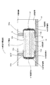
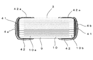
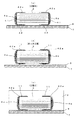
図1に示す本実施形態の部品内蔵基板1Aは、樹脂からなる絶縁層2に1個又は複数個のチップ部品3を埋設し、各チップ部品3の左、右の両端面に形成された外部電極4a、4bを、ビア5(又はスルーホール)を通して絶縁層2上の電極層6に電気的に接続した構成である。
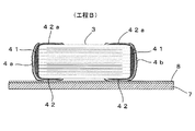
つぎに、部品内蔵基板1Aの製造方法の工程順を追って図1及び図3〜図7を参照して説明する。
つぎに、他の実施形態について、図8、図9を参照して説明する。
本実施形態の部品内蔵基板1Bが前記実施形態の部品内蔵基板1Aと異なる点は、図8に示すように、チップ部品3の外部電極4a、4bにおいて、上面側の延長部分42のうち平坦化されたビア5の形成位置42aの表面が、銅(Cu)又は銀(Ag)或いはそれらの合金のめっき11により極めて平坦な鏡面に形成されている点である。
つぎに、部品内蔵基板1Bの製造方法について、図9を参照して説明する。
2 絶縁層
3 チップ部品
4a、4b 外部電極
41 端面部分
42 延長部分
5 ビア
6 電極層
11 めっき
Claims (4)
- 内部電極を有する絶縁体と、該絶縁体の両端に形成され、前記内部電極と接続された外部電極とを備え、前記外部電極が前記絶縁体の端面を覆う端面部分と、該端面部分から前記絶縁体の側面に延出した縁状の延長部分とからなるチップ部品を用意し、前記延長部分のうち少なくとも一部を、表面粗さの指標Rzにおいて、0<Rz<5μmを満たすように平坦化する第一の工程と、
前記チップ部品を配線板上に固定する第二の工程と、
前記外部電極が平坦化された前記チップ部品を絶縁層に埋設する第三の工程と、
前記外部電極の平坦化された面を底面として、前記絶縁層にビアまたはスルーホールを形成する第四の工程と、
前記絶縁層上に、前記ビアまたはスルーホールに電気的に接続される電極層を形成する第五の工程と
を備えたことを特徴とする部品内蔵基板の製造方法。 - 請求項1に記載の部品内蔵基板の製造方法において、
前記第一の工程に替えて、内部電極を有する絶縁体と、該絶縁体の両端に形成され、前記内部電極と接続された外部電極とを備え、前記外部電極が前記絶縁体の端面を覆う端面部分と、該端面部分から前記絶縁体の側面に延出した縁状の延長部分とからなるチップ部品を用意する工程を備え、
前記第二の工程により、用意した前記チップ部品を配線板上に固定して前記延長部分のうち少なくとも一部を、表面粗さの指標Rzにおいて、0<Rz<5μmを満たすように平坦化することを特徴とする部品内蔵基板の製造方法。 - 請求項1又は2に記載の部品内蔵基板の製造方法において、
前記平坦化は、平面研磨によってなされることを特徴とする部品内蔵基板の製造方法。 - 請求項1〜3のいずれか一項に記載の部品内蔵基板の製造方法において、
前記第三の工程の前に、少なくとも前記平坦化された面を含む前記外部電極に、銅又は銀或いはそれらの合金のめっきを施す工程をさらに備えたことを特徴とする部品内蔵基板の製造方法。
Priority Applications (1)
| Application Number | Priority Date | Filing Date | Title |
|---|---|---|---|
| JP2011234623A JP2012019247A (ja) | 2007-06-15 | 2011-10-26 | 部品内蔵基板の製造方法 |
Applications Claiming Priority (3)
| Application Number | Priority Date | Filing Date | Title |
|---|---|---|---|
| JP2007158995 | 2007-06-15 | ||
| JP2007158995 | 2007-06-15 | ||
| JP2011234623A JP2012019247A (ja) | 2007-06-15 | 2011-10-26 | 部品内蔵基板の製造方法 |
Related Parent Applications (1)
| Application Number | Title | Priority Date | Filing Date |
|---|---|---|---|
| JP2009520404A Division JP5007746B2 (ja) | 2007-06-15 | 2008-05-20 | 部品内蔵基板 |
Publications (1)
| Publication Number | Publication Date |
|---|---|
| JP2012019247A true JP2012019247A (ja) | 2012-01-26 |
Family
ID=40156126
Family Applications (2)
| Application Number | Title | Priority Date | Filing Date |
|---|---|---|---|
| JP2009520404A Active JP5007746B2 (ja) | 2007-06-15 | 2008-05-20 | 部品内蔵基板 |
| JP2011234623A Pending JP2012019247A (ja) | 2007-06-15 | 2011-10-26 | 部品内蔵基板の製造方法 |
Family Applications Before (1)
| Application Number | Title | Priority Date | Filing Date |
|---|---|---|---|
| JP2009520404A Active JP5007746B2 (ja) | 2007-06-15 | 2008-05-20 | 部品内蔵基板 |
Country Status (2)
| Country | Link |
|---|---|
| JP (2) | JP5007746B2 (ja) |
| WO (1) | WO2008155967A1 (ja) |
Cited By (2)
| Publication number | Priority date | Publication date | Assignee | Title |
|---|---|---|---|---|
| JP2014131006A (ja) * | 2012-12-27 | 2014-07-10 | Samsung Electro-Mechanics Co Ltd | 電子部品内蔵印刷回路基板及びその製造方法 |
| JPWO2015029783A1 (ja) * | 2013-08-29 | 2017-03-02 | 株式会社村田製作所 | 部品一体型シートの製造方法、電子部品を内蔵した樹脂多層基板の製造方法、ならびに樹脂多層基板 |
Families Citing this family (7)
| Publication number | Priority date | Publication date | Assignee | Title |
|---|---|---|---|---|
| WO2011071111A1 (ja) * | 2009-12-09 | 2011-06-16 | 株式会社村田製作所 | 電子部品内蔵樹脂基板および電子回路モジュール |
| JP2012204831A (ja) * | 2011-03-23 | 2012-10-22 | Ibiden Co Ltd | 電子部品内蔵配線板及びその製造方法 |
| JP6528258B2 (ja) * | 2014-04-25 | 2019-06-12 | 国立研究開発法人産業技術総合研究所 | 部品内蔵基板 |
| JP6418099B2 (ja) * | 2014-09-01 | 2018-11-07 | 株式会社村田製作所 | 電子部品内蔵基板 |
| JP2016149484A (ja) * | 2015-02-13 | 2016-08-18 | Tdk株式会社 | 積層コンデンサ |
| JP6867745B2 (ja) * | 2015-02-13 | 2021-05-12 | Tdk株式会社 | 積層コンデンサ及び積層コンデンサの実装構造 |
| JP6731681B2 (ja) * | 2019-04-24 | 2020-07-29 | 国立研究開発法人産業技術総合研究所 | 部品内蔵基板 |
Citations (5)
| Publication number | Priority date | Publication date | Assignee | Title |
|---|---|---|---|---|
| JP2001345560A (ja) * | 2000-02-09 | 2001-12-14 | Ngk Spark Plug Co Ltd | 配線基板およびその製造方法、並びに電子部品 |
| JP2001352141A (ja) * | 2000-04-05 | 2001-12-21 | Ibiden Co Ltd | プリント配線板及びプリント配線板の製造方法 |
| JP2002100875A (ja) * | 1999-09-02 | 2002-04-05 | Ibiden Co Ltd | プリント配線板およびコンデンサ |
| JP2003249414A (ja) * | 2002-02-25 | 2003-09-05 | Kyocera Corp | コンデンサ素子およびコンデンサ素子内蔵多層配線基板 |
| JP2005236067A (ja) * | 2004-02-20 | 2005-09-02 | Dainippon Printing Co Ltd | 配線基板と配線基板の製造方法、および半導パッケージ |
Family Cites Families (2)
| Publication number | Priority date | Publication date | Assignee | Title |
|---|---|---|---|---|
| JPH08144083A (ja) * | 1994-11-17 | 1996-06-04 | Taiyo Yuden Co Ltd | 電子部品のメッキ後処理方法 |
| JP3888446B2 (ja) * | 2002-03-25 | 2007-03-07 | 株式会社村田製作所 | セラミック電子部品、及びセラミック電子部品の製造方法 |
-
2008
- 2008-05-20 WO PCT/JP2008/059165 patent/WO2008155967A1/ja not_active Ceased
- 2008-05-20 JP JP2009520404A patent/JP5007746B2/ja active Active
-
2011
- 2011-10-26 JP JP2011234623A patent/JP2012019247A/ja active Pending
Patent Citations (5)
| Publication number | Priority date | Publication date | Assignee | Title |
|---|---|---|---|---|
| JP2002100875A (ja) * | 1999-09-02 | 2002-04-05 | Ibiden Co Ltd | プリント配線板およびコンデンサ |
| JP2001345560A (ja) * | 2000-02-09 | 2001-12-14 | Ngk Spark Plug Co Ltd | 配線基板およびその製造方法、並びに電子部品 |
| JP2001352141A (ja) * | 2000-04-05 | 2001-12-21 | Ibiden Co Ltd | プリント配線板及びプリント配線板の製造方法 |
| JP2003249414A (ja) * | 2002-02-25 | 2003-09-05 | Kyocera Corp | コンデンサ素子およびコンデンサ素子内蔵多層配線基板 |
| JP2005236067A (ja) * | 2004-02-20 | 2005-09-02 | Dainippon Printing Co Ltd | 配線基板と配線基板の製造方法、および半導パッケージ |
Cited By (7)
| Publication number | Priority date | Publication date | Assignee | Title |
|---|---|---|---|---|
| JP2014131006A (ja) * | 2012-12-27 | 2014-07-10 | Samsung Electro-Mechanics Co Ltd | 電子部品内蔵印刷回路基板及びその製造方法 |
| JP2014239258A (ja) * | 2012-12-27 | 2014-12-18 | サムソン エレクトロ−メカニックス カンパニーリミテッド. | 電子部品内蔵印刷回路基板の製造方法 |
| JP2015179879A (ja) * | 2012-12-27 | 2015-10-08 | サムソン エレクトロ−メカニックス カンパニーリミテッド. | 電子部品内蔵印刷回路基板 |
| TWI504321B (zh) * | 2012-12-27 | 2015-10-11 | 三星電機股份有限公司 | 具有嵌入式電子元件之印刷電路板及其製造方法 |
| US10015884B2 (en) | 2012-12-27 | 2018-07-03 | Samsung Electro-Mechanics Co., Ltd. | Printed circuit board including embedded electronic component and method for manufacturing the same |
| US10887995B2 (en) | 2012-12-27 | 2021-01-05 | Samsung Electro-Mechanics Co., Ltd. | Method for manufacturing a printed circuit board including an embedded electronic component |
| JPWO2015029783A1 (ja) * | 2013-08-29 | 2017-03-02 | 株式会社村田製作所 | 部品一体型シートの製造方法、電子部品を内蔵した樹脂多層基板の製造方法、ならびに樹脂多層基板 |
Also Published As
| Publication number | Publication date |
|---|---|
| JP5007746B2 (ja) | 2012-08-22 |
| JPWO2008155967A1 (ja) | 2010-08-26 |
| WO2008155967A1 (ja) | 2008-12-24 |
Similar Documents
| Publication | Publication Date | Title |
|---|---|---|
| JP2012019247A (ja) | 部品内蔵基板の製造方法 | |
| JP3910045B2 (ja) | 電子部品内装配線板の製造方法 | |
| KR101975133B1 (ko) | 전자 부품의 제조 방법 및 전자 부품 | |
| JP7074409B2 (ja) | 素子内蔵型印刷回路基板 | |
| TWI466606B (zh) | 具有內埋元件的電路板及其製作方法 | |
| JPWO2008155957A1 (ja) | 部品内蔵基板の製造方法および部品内蔵基板 | |
| US9480172B2 (en) | Method for producing a printed circuit board consisting of at least two printed circuit board regions, and printed circuit board | |
| JP2014232862A (ja) | 印刷回路基板 | |
| US20200120805A1 (en) | Embedded circuit board and method of making same | |
| CN108811320A (zh) | 电子模块与电路板 | |
| US9596765B2 (en) | Manufacturing method for component incorporated substrate and component incorporated substrate manufactured using the method | |
| US20140209361A1 (en) | Wiring board and method for manufacturing the same | |
| JP2009010266A (ja) | プリント配線板の製造方法及びプリント配線板 | |
| JP2007189066A (ja) | 電子部品の製造方法及び電子部品の基板集合体 | |
| JP2014232812A (ja) | プリント配線板およびその製造方法 | |
| KR100752017B1 (ko) | 인쇄회로기판의 제조방법 | |
| CN115209609A (zh) | 埋入元件的多层线路板及线路板的制作方法 | |
| CN209861268U (zh) | 同时具有贯孔及盲孔的多层电路板结构 | |
| JP5037970B2 (ja) | 電子部品収納基板 | |
| JP2015204379A (ja) | プリント配線板 | |
| KR100653247B1 (ko) | 내장된 전기소자를 구비한 인쇄회로기판 및 그 제작방법 | |
| JP2006049457A (ja) | 部品内蔵配線板、部品内蔵配線板の製造方法 | |
| JP2002026519A (ja) | プリント回路基板及びその製造方法 | |
| JP4701853B2 (ja) | 抵抗素子を内蔵した多層配線基板及び抵抗素子の抵抗値調整方法 | |
| JP4522282B2 (ja) | 多層フレキシブル回路配線基板の製造方法 |
Legal Events
| Date | Code | Title | Description |
|---|---|---|---|
| A621 | Written request for application examination |
Free format text: JAPANESE INTERMEDIATE CODE: A621 Effective date: 20111114 |
|
| A977 | Report on retrieval |
Free format text: JAPANESE INTERMEDIATE CODE: A971007 Effective date: 20130110 |
|
| A131 | Notification of reasons for refusal |
Free format text: JAPANESE INTERMEDIATE CODE: A131 Effective date: 20130115 |
|
| A521 | Request for written amendment filed |
Free format text: JAPANESE INTERMEDIATE CODE: A523 Effective date: 20130306 |
|
| A131 | Notification of reasons for refusal |
Free format text: JAPANESE INTERMEDIATE CODE: A131 Effective date: 20130903 |
|
| A02 | Decision of refusal |
Free format text: JAPANESE INTERMEDIATE CODE: A02 Effective date: 20140114 |