JP2012068043A - Electric inspection device and method for planar circuit board - Google Patents
Electric inspection device and method for planar circuit board Download PDFInfo
- Publication number
- JP2012068043A JP2012068043A JP2010210721A JP2010210721A JP2012068043A JP 2012068043 A JP2012068043 A JP 2012068043A JP 2010210721 A JP2010210721 A JP 2010210721A JP 2010210721 A JP2010210721 A JP 2010210721A JP 2012068043 A JP2012068043 A JP 2012068043A
- Authority
- JP
- Japan
- Prior art keywords
- circuit board
- planar circuit
- probe pins
- probe
- pin
- Prior art date
- Legal status (The legal status is an assumption and is not a legal conclusion. Google has not performed a legal analysis and makes no representation as to the accuracy of the status listed.)
- Pending
Links
Images



Landscapes
- Measuring Leads Or Probes (AREA)
- Testing Of Short-Circuits, Discontinuities, Leakage, Or Incorrect Line Connections (AREA)
- Tests Of Electronic Circuits (AREA)
Abstract
【課題】平面回路基板の種類によらず同一装置により検査を行うこと。
【解決手段】電気検査装置2は、平面回路基板1に対向可能に配置され、所定の規則により一様に配列された多数のプローブピン3と、多数のプローブピン3を支持すると共に、多数のプローブピン3を平面回路基板1に対して移動させるためのピンボード4と、各プローブピン3に接続され、各プローブピン3からの信号に基づき平面回路基板1の電気的特性を計測するための計測部12等と、各プローブピン3を、計測部12等に対して選択的に接続するための接続切替部15と、電源部13と、通信部14と、制御部11とを備える。平面回路基板1上に形成されたプローブピン3と接触可能な検査点37A〜37Hの配置は、多数のプローブピン3の配列に整合するように予め配置される。
【選択図】 図1An inspection is performed by the same apparatus regardless of the type of the planar circuit board.
An electrical inspection device 2 is arranged so as to face a planar circuit board 1 and supports a large number of probe pins 3 arranged uniformly according to a predetermined rule, and a large number of probe pins 3. A pin board 4 for moving the probe pin 3 with respect to the planar circuit board 1 and connected to each probe pin 3 for measuring electrical characteristics of the planar circuit board 1 based on signals from each probe pin 3 The measurement unit 12 and the like, a connection switching unit 15 for selectively connecting each probe pin 3 to the measurement unit 12 and the like, a power supply unit 13, a communication unit 14, and a control unit 11 are provided. The arrangement of the inspection points 37 </ b> A to 37 </ b> H that can come into contact with the probe pins 3 formed on the planar circuit board 1 is arranged in advance so as to match the arrangement of a large number of probe pins 3.
[Selection] Figure 1
Description
この発明は、回路素子と配線を基板上に平面的に形成してなる平面回路基板につき、電気的な検査を行うために使用される平面回路基板の電気検査装置及び電気検査方法に関する。 The present invention relates to an electrical inspection apparatus and an electrical inspection method for a planar circuit board used for electrical inspection of a planar circuit board formed by planarly forming circuit elements and wirings on the substrate.
従来、この種の技術として、例えば、下記の特許文献1に記載の装置が知られている。この装置では、検査ユニットがそれぞれ多針状に構成された複数の接触子を備える。これらの接触子は、基板上の配線パターンにおけるランドやパッド等の検査点の位置に対応して配置され、保持されている。下記の特許文献2には、関連技術が記載されている。
Conventionally, as this type of technology, for example, an apparatus described in
ここで、「基板」として、プリント配線基板、フレキシブル基板、多層配線基板、液晶ディスプレイ用の電極板、半導体パッケージ用のパッケージ基板やフィルムキャリアなど種々の基板が想定されている。 Here, as the “substrate”, various substrates such as a printed circuit board, a flexible circuit board, a multilayer circuit board, an electrode plate for a liquid crystal display, a package substrate for a semiconductor package, and a film carrier are assumed.
また、特許文献2には、個別部品を半田付け等により回路基板に実装した製品を検査するために、多数のプローブピンを配設したピンボードを用いた電気検査の一例が記載されている。 Patent Document 2 describes an example of electrical inspection using a pin board provided with a large number of probe pins in order to inspect a product in which individual components are mounted on a circuit board by soldering or the like.
ところが、特許文献1に記載の装置では、基板の種類の違いにより検査点の位置が変わることがある。このため、基板の種類が異なることで、接触子の配置を変える必要があり、段替工数がかかり、ミスが生じるおそれもあった。
However, in the apparatus described in
また、特許文献2に記載の検査方法では、部品との接触を避けるように、プローブピンをピンボードに配置している。ここで、製品の種類が増え、部品配置の変更があると、部品との干渉を避けるため、プローブピンの配置を変えてピンボードを作り直す必要があった。このため、実際には、プリント基板の種類が増えるという制約の中で一定の種類に収める必要があった。 In the inspection method described in Patent Document 2, probe pins are arranged on a pin board so as to avoid contact with components. Here, when the types of products increase and the component arrangement is changed, it is necessary to change the arrangement of the probe pins and recreate the pin board in order to avoid interference with the components. For this reason, in practice, it has been necessary to keep the printed circuit board in a certain type under the constraint that the number of printed circuit board types increases.
この発明は、上記事情に鑑みてなされたものであり、特に、平面回路基板に特化した検査に着目してなされたものであって、その目的は、平面回路基板の種類によらず同一装置により検査を行うことを可能とした平面回路基板の電気検査装置及び電気検査方法を提供することにある。 The present invention has been made in view of the above circumstances, and in particular, has been made by paying attention to the inspection specialized in the planar circuit board, and the purpose thereof is the same apparatus regardless of the type of the planar circuit board. It is an object of the present invention to provide an electrical inspection apparatus and electrical inspection method for a planar circuit board that can be inspected by the above.
上記目的を達成するために、請求項1に記載の発明は、平面回路基板に対向可能に配置され、所定の規則により一様に配列された多数のプローブピンと、多数のプローブピンを支持すると共に、多数のプローブピンを平面回路基板に対して移動させるためのピンボードと、各プローブピンに接続され、各プローブピンからの信号に基づき平面回路基板の電気的特性を計測するための計測手段と、各プローブピンを、計測手段に対して選択的に接続するための接続切替手段とを備えたことを趣旨とする。
In order to achieve the above object, the invention according to
上記発明の構成によれば、多数のプローブピンを所定の規則により一様に配列してピンボードに支持し、その配列の一部と整合するように平面回路基板の検査点を予め配置しておく。これにより、多数のプローブピンの一部を、平面回路基板の検査点に接触させることが可能となる。ここで、「平面回路基板」は、回路素子と配線を基板上に平面的に形成して構成されたものであり、回路素子及び配線は、例えば、基板に対し印刷により形成される。 According to the configuration of the invention, a large number of probe pins are uniformly arranged according to a predetermined rule and supported on the pin board, and the inspection points of the planar circuit board are arranged in advance so as to be aligned with a part of the arrangement. deep. This makes it possible to bring some of the many probe pins into contact with the inspection points on the planar circuit board. Here, the “planar circuit board” is configured by planarly forming circuit elements and wirings on the substrate, and the circuit elements and wirings are formed, for example, by printing on the substrate.
上記目的を達成するために、請求項2に記載の発明は、請求項1に記載の発明において、多数のプローブピンの配列に係る所定の規則を、一単位の配列が正方形をなすようにすることが好ましい。 In order to achieve the above object, according to a second aspect of the present invention, in the first aspect of the present invention, the predetermined rule relating to the arrangement of a plurality of probe pins is made such that one unit of the arrangement forms a square. It is preferable.
上記目的を達成するために、請求項3に記載の発明は、請求項1に記載の発明において、多数のプローブピンの配列に係る所定の規則を、一単位の配列が正三角をなすようにすることが好ましい。
To achieve the above object, the invention according to
上記目的を達成するために、請求項4に記載の発明は、所定の規則により一様に配列された多数のプローブピンの先端を、平面回路基板上に接触させ、多数のプローブピンのうち、平面回路基板上に形成された複数の検査点に接触しているプローブピンのみにつき選択的に切り替えて計測部に接続し、電気的特性を計測することにより平面回路基板を検査することを趣旨とする。
In order to achieve the above object, the invention according to
上記発明の構成によれば、上記発明の構成によれば、多数のプローブピンを所定の規則により一様に配列してピンボードに支持し、その配列の一部と整合するように平面回路基板の検査点を予め配置しておく。これにより、多数のプローブピンの一部を、平面回路基板の検査点に接触させることが可能となる。 According to the configuration of the above invention, according to the configuration of the above invention, the planar circuit board is arranged so that a large number of probe pins are uniformly arranged according to a predetermined rule and supported on the pin board and aligned with a part of the arrangement. The inspection points are arranged in advance. This makes it possible to bring some of the many probe pins into contact with the inspection points on the planar circuit board.
この発明によれば、平面回路基板の種類によらず同一装置を汎用的に使用して平面回路基板の電気的特性を検査することができる。 According to the present invention, the electrical characteristics of the planar circuit board can be inspected using the same apparatus for general purposes regardless of the type of the planar circuit board.
以下、本発明における平面回路基板の電気検査装置及び電気検査方法を具体化した一実施形態につき図面を参照して詳細に説明する。 Hereinafter, an embodiment of an electrical inspection apparatus and electrical inspection method for a planar circuit board according to the present invention will be described in detail with reference to the drawings.
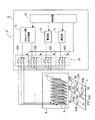
図1に、この実施形態の平面回路基板1と電気検査装置2の電気的構成を概略図により示す。この電気検査装置2は、平面回路基板1に対向可能に配置され、所定の規則により一様に配列された多数のプローブピン3と、それら多数のプローブピン3を支持すると共に、多数のプローブピン3を平面回路基板1に対して移動させるためのピンボード4と、計測装置5とを備える。計測装置5は、制御部11、ADコンバータ等の計測部12、電源部13、通信部14及び接続切替部15を備える。制御部11、計測部12、電源部13及び通信部14は、本発明の計測手段に相当する。接続切替部15は、本発明の接続切替手段に相当する。
FIG. 1 schematically shows the electrical configuration of the
制御部11は、計測部12、電源部13、通信部14及び接続切替部15をそれぞれ制御するようになっている。制御部11は、中央処理装置(CPU)及びメモリを備え、メモリには、所定の制御プログラムが格納される。
The
接続切替部15は、第1〜第4のスイッチング回路16A〜16Dから構成される。各スイッチング回路16A〜16Dは、それぞれ各プローブピン3に電気的に接続される。各スイッチング回路16A〜16Dは、各プローブピン3を、計測部12、電源部13及び通信部14に対して選択的に接続するように構成される。
The
計測部12は、ADコンバータ等を含み、第1及び第2のスイッチング回路16A,16Bを介して各プローブピン3に接続される。計測部12は、各プローブピン3からの信号に基づき平面回路基板1の電気的特性を計測するように構成される。
The
電源部13は、第3のスイッチング回路16Cを介して各プローブピン3に接続される。電源部13は、各プローブピン3に電源を供給するように構成される。
The
通信部14は、第4のスイッチング回路16Dを介して各プローブピン3に接続される。通信部14は、各プローブピン3を介して平面回路基板1との間で通信を行い、平面回路基板1上の素子32による計測値を受信するように構成される。
The
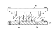
図2,3に、この電気検査装置2の機械的構成の概略を断面図により示す。この装置2は、平面回路基板1を水平に支持する支持台21と、多数のプローブピン3を一体的に支持するピンボード4と、ピンボード4を支持棒22を介して水平に支持する機構ケース23とを備える。機構ケース23は、図示していない昇降機構により上下動可能に構成される。
2 and 3 are schematic sectional views showing the mechanical configuration of the electrical inspection apparatus 2. The apparatus 2 includes a
そして、図2に示す状態から、昇降機構により機構ケース23を下降させることにより、図3に示すように、各プローブピン3の先端を、平面回路基板1上に多少の加圧状態で当接させることができる。
Then, by lowering the
ピンボード4には、複数のガイドバー24が下方へ向けて設けられる。また、支持台21には、各ガイドバー24に整合する複数のガイド孔25が設けられる。各ガイドバー24は、図2に示すように、ピンボード4が支持台21から離れた状態から、図3に示すように、ピンボード4が支持台21に近付いたときに、支持台21の各ガイド孔25に挿入され、支持台21とピンボード4が一体的に位置決めされるようになっている。
The
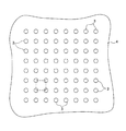
図4に、ピンボード4における多数のプローブピン3の一部の配列状態を拡大して平面図により示す。多数のプローブピン3の配列に係る所定の規則は、図4に2点鎖線で示すように、一単位の配列が正方形をなすように構成される。ピンボード4には、例えば、1000〜1500本のプローブピン3が設けられる。この実施形態では、隣り合うプローブピン3同士の間隔として、例えば「2〜2.5(mm)」程度の寸法が想定される。
FIG. 4 is an enlarged plan view showing a partial arrangement state of a large number of probe pins 3 on the
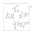
図5に、平面回路基板1を拡大して平面図により示す。この平面回路基板1は、複数の回路素子31,32,33,34と配線35を基板36上に平面的に形成して構成される。この実施形態で、各回路素子31〜34及び配線35は、基板36に対し印刷により形成される。印刷はインクジェットやスクリーン印刷などの手法を用いて行われる。配線35上には、所々に導電性を有する複数の検査点37A,37B,37C,37D,37E,37F,37G,37Hが形成される。各検査点37A〜37Hを除き、基板36の上面は絶縁性皮膜(図示略)で覆われ保護される。
FIG. 5 is an enlarged plan view of the
この実施形態で、上記した各検査点37A〜37Hの配置は、ピンボード4に支持された多数のプローブピン3の配列に整合している。図6に、基板36上に形成された回路素子31〜34、配線35及び検査点37A〜37Hの配置と、多数のプローブピン3の配列との関係を平面図により示す。図6から明らかなように、各検査点37A〜37Hは、一部のプローブピン3の配列と一致することが分かる。すなわち、この実施形態では、平面回路基板1上の各検査点37A〜37Hが、ピンボード4に支持された多数のプローブピン3の配列に合わせて形成されているのである。
In this embodiment, the arrangement of the inspection points 37 </ b> A to 37 </ b> H described above matches the arrangement of a large number of probe pins 3 supported by the
次に、上記した電気検査装置2を使用して行われる検査方法について説明する。この検査は、図3に示すように、各プローブピン3を平面回路基板1上に加圧状態で当接させて行われる。図7に、制御部11が実行する制御プログラムをフローチャートにより示す。
Next, an inspection method performed using the above-described electrical inspection apparatus 2 will be described. As shown in FIG. 3, this inspection is performed by bringing each
ステップ100で、制御部11は、計測確認を実行する。すなわち、制御部11は、接続切替部15を切り替え、電源部13から各プローブピン3を介して平面回路基板1へ微小電圧を印加し、所定の電流が計測されるかを計測部12により確認させる。このステップで、平面回路基板1の回路にオープンやショートがないかを確認する。
In
ステップ110で、制御部11は、第1の通信結果確認を実行する。すなわち、制御部11は、接続切替部15を切り替え、電源部13から各プローブピン3を介して平面回路基板1へ電源を供給し、通信部14を各プローブピン3を介して平面回路基板1と接続し、所定の通信結果が得られるかを通信部14により確認させる。このステップで、回路素子32が正常に動作するかを確認する。
In
ステップ120で、制御部11は、第1の電圧確認を実行する。すなわち、制御部11は、接続切替部15を切り替え、電源部13から各プローブピン3を介して平面回路基板1へ電源を供給し、通信部14を各プローブピン3を介して平面回路基板1と接続し、出力端子を所定の状態に設定した後、所定の電圧が計測されるかを計測部12により確認させる。このステップで出力回路が正常に動作するかを確認する。
In
ステップ130で、制御部11は、第2の通信結果確認を実行する。すなわち、制御部11は、接続切替部15を切り替え、電源部13から各プローブピン3を介して平面回路基板1へ電源を供給し、通信部14を各プローブピン3を介して平面回路基板1と接続し、検査点37Aに電圧を印加して所定の通信結果が得られるかを通信部14により確認させる。このステップで、入力回路が正常に動作するかを確認する。
In
ステップ140で、制御部11は、第2の電圧確認を実行する。すなわち、制御部11は、接続切替部15を切り替え、電源部13から各プローブピン3を介して平面回路基板1へ電源を供給し、通信部14を各プローブピン3を介して平面回路基板1と接続し、検査点37Aに電圧を印加して検査点37Fに所定の電圧が出力されるかを計測部12で確認する。このステップで平面回路基板1の全体の電気的特性を検査し、平面回路基板1の動作が正常であるか否かを確認する。
In
上記したように、この実施形態では、所定の規則により一様に配列された多数のプローブピン3の先端を、平面回路基板1上に接触させ、多数のプローブピン3のうち、平面回路基板1上に形成された複数の検査点に接触しているプローブピン3を選択的に切り替えて計測部12に接続し、電気的特性を計測することにより平面回路基板1を検査する電気検査方法を実施するようにしている。
As described above, in this embodiment, the tips of a large number of probe pins 3 arranged uniformly according to a predetermined rule are brought into contact with the
以上説明したこの実施形態の電気検査装置2及び電気検査方法によれば、多数のプローブピン3を所定の規則により一様に配列してピンボード4に支持し、その配列の一部と整合するように平面回路基板1の各検査点37A〜37Hを予め配置するようにしている。これにより、多数のプローブピン3の一部を、平面回路基板1の各検査点37A〜37Hに接触させることが可能となる。このため、平面回路基板1の種類によらず同一の電気検査装置2を汎用的に使用して平面回路基板1の電気的特性の検査を行うことができる。すなわち、従来は、ピンボードを回路基板の製品毎に合わせて作成する必要があった。これに対し、この実施形態の電気検査装置2によれば、平面回路基板1上の、プローブピン3の配列と整合する位置に、各検査点37A〜37Hを配置することで、どのような製品(平面回路基板1)でも、ピンボードを別途設けることなく、同一のピンボード4を汎用的に使用して平面回路基板1の検査を行うことができる。
According to the electrical inspection apparatus 2 and the electrical inspection method of this embodiment described above, a large number of probe pins 3 are uniformly arranged according to a predetermined rule and supported on the
なお、この発明は前記実施形態に限定されるものではなく、発明の趣旨を逸脱することのない範囲で構成の一部を適宜変更することにより実施することができる。 In addition, this invention is not limited to the said embodiment, It can implement by changing a part of structure suitably in the range which does not deviate from the meaning of invention.
例えば、前記実施形態では、多数のプローブピン3の配列に係る所定の規則を、図4に示すように、一単位の配列が正方形をなすように構成した。これに対し、多数のプローブピン3の配列に係る所定の規則を、図8に示すように、一単位の配列が正三角をなすように構成することもできる。 For example, in the above-described embodiment, the predetermined rule relating to the arrangement of a large number of probe pins 3 is configured such that one unit arrangement forms a square as shown in FIG. On the other hand, as shown in FIG. 8, the predetermined rule concerning the arrangement of a large number of probe pins 3 can be configured such that the arrangement of one unit forms a regular triangle.
この発明は、平面回路基板の電気的特性に係る検査に利用することができる。 The present invention can be used for inspection relating to the electrical characteristics of a planar circuit board.
1 平面回路基板
2 電気検査装置
3 プローブピン
4 ピンボード
11 制御部(計測手段)
12 計測部(計測手段)
13 電源部(計測手段)
14 通信部(計測手段)
15 接続切替部(切替手段)
31 回路素子
32 回路素子
33 回路素子
34 回路素子
35 配線
36 基板
37A 検査点
37B 検査点
37C 検査点
37D 検査点
37E 検査点
37F 検査点
37G 検査点
37H 検査点
DESCRIPTION OF
12 Measuring unit (measuring means)
13 Power supply (measuring means)
14 Communication unit (measuring means)
15 Connection switching part (switching means)
31
Claims (4)
前記多数のプローブピンを支持すると共に、前記多数のプローブピンを前記平面回路基板に対して移動させるためのピンボードと、
前記各プローブピンに接続され、前記各プローブピンからの信号に基づき前記平面回路基板の電気的特性を計測するための計測手段と、
前記各プローブピンを、前記計測手段に対して選択的に接続するための接続切替手段と
を備えたことを特徴とする平面回路基板の電気検査装置。 A large number of probe pins arranged so as to face the planar circuit board and uniformly arranged according to a predetermined rule;
A pin board for supporting the multiple probe pins and moving the multiple probe pins relative to the planar circuit board;
Measuring means connected to each probe pin and measuring the electrical characteristics of the planar circuit board based on signals from each probe pin;
An electrical inspection apparatus for a planar circuit board, comprising: a connection switching means for selectively connecting the probe pins to the measuring means.
Priority Applications (1)
| Application Number | Priority Date | Filing Date | Title |
|---|---|---|---|
| JP2010210721A JP2012068043A (en) | 2010-09-21 | 2010-09-21 | Electric inspection device and method for planar circuit board |
Applications Claiming Priority (1)
| Application Number | Priority Date | Filing Date | Title |
|---|---|---|---|
| JP2010210721A JP2012068043A (en) | 2010-09-21 | 2010-09-21 | Electric inspection device and method for planar circuit board |
Publications (1)
| Publication Number | Publication Date |
|---|---|
| JP2012068043A true JP2012068043A (en) | 2012-04-05 |
Family
ID=46165503
Family Applications (1)
| Application Number | Title | Priority Date | Filing Date |
|---|---|---|---|
| JP2010210721A Pending JP2012068043A (en) | 2010-09-21 | 2010-09-21 | Electric inspection device and method for planar circuit board |
Country Status (1)
| Country | Link |
|---|---|
| JP (1) | JP2012068043A (en) |
Cited By (3)
| Publication number | Priority date | Publication date | Assignee | Title |
|---|---|---|---|---|
| JP2014106168A (en) * | 2012-11-29 | 2014-06-09 | Micronics Japan Co Ltd | Probe assembly and probe substrate |
| JP2018524745A (en) * | 2015-05-22 | 2018-08-30 | パワー フィンガープリンティング インコーポレイテッド | Systems, methods and equipment for intrusion detection and analysis using power characteristics such as side channel information |
| JP2021189085A (en) * | 2020-06-02 | 2021-12-13 | 東理システム株式会社 | Electric characteristic inspection unit of power conversion circuit device and current test probe of electrical characteristic inspection unit |
Citations (2)
| Publication number | Priority date | Publication date | Assignee | Title |
|---|---|---|---|---|
| JP2003240812A (en) * | 2002-02-14 | 2003-08-27 | Taiyo Kogyo Kk | Inspection fixture and inspection method using it |
| JP2006133199A (en) * | 2004-11-09 | 2006-05-25 | Tnk Incubation:Kk | Spring contact probe device |
-
2010
- 2010-09-21 JP JP2010210721A patent/JP2012068043A/en active Pending
Patent Citations (2)
| Publication number | Priority date | Publication date | Assignee | Title |
|---|---|---|---|---|
| JP2003240812A (en) * | 2002-02-14 | 2003-08-27 | Taiyo Kogyo Kk | Inspection fixture and inspection method using it |
| JP2006133199A (en) * | 2004-11-09 | 2006-05-25 | Tnk Incubation:Kk | Spring contact probe device |
Cited By (6)
| Publication number | Priority date | Publication date | Assignee | Title |
|---|---|---|---|---|
| JP2014106168A (en) * | 2012-11-29 | 2014-06-09 | Micronics Japan Co Ltd | Probe assembly and probe substrate |
| JP2018524745A (en) * | 2015-05-22 | 2018-08-30 | パワー フィンガープリンティング インコーポレイテッド | Systems, methods and equipment for intrusion detection and analysis using power characteristics such as side channel information |
| US10970387B2 (en) | 2015-05-22 | 2021-04-06 | Power Fingerprinting Inc. | Systems, methods, and apparatuses for intrusion detection and analytics using power characteristics such as side-channel information collection |
| US11809552B2 (en) | 2015-05-22 | 2023-11-07 | Power Fingerprinting Inc. | Systems, methods, and apparatuses for intrusion detection and analytics using power characteristics such as side-channel information collection |
| JP2021189085A (en) * | 2020-06-02 | 2021-12-13 | 東理システム株式会社 | Electric characteristic inspection unit of power conversion circuit device and current test probe of electrical characteristic inspection unit |
| JP7175518B2 (en) | 2020-06-02 | 2022-11-21 | 東理システム株式会社 | Electrical characteristic inspection unit device for power conversion circuit devices |
Similar Documents
| Publication | Publication Date | Title |
|---|---|---|
| JP5396112B2 (en) | Probe card | |
| KR102422188B1 (en) | Vertical Probe Array with Tiled Membrane Space Transformers | |
| CN101071140A (en) | Probe, testing head having a plurality of probes, and circuit board tester having the testing head | |
| JP2007178318A (en) | Substrate inspection device and method | |
| KR100884475B1 (en) | Display panel inspection device | |
| JP2013088288A (en) | Inspection device and inspection system | |
| JP6570354B2 (en) | Circuit board inspection apparatus and contact check method | |
| JP6285292B2 (en) | Probe card and inspection device | |
| WO2008001651A1 (en) | Board inspecting method and board inspecting device | |
| JP2000221227A (en) | Apparatus and method for inspecting conductive pattern | |
| KR101559984B1 (en) | Probe card, testing apparatus and testing method | |
| CN113109696A (en) | Method for testing performance of PCB conductive hole | |
| JP2008039725A (en) | Electrical inspection method for printed wiring board and electrical inspection apparatus for printed wiring board | |
| JP2008039725A5 (en) | ||
| KR101416882B1 (en) | Probe pin contact check system of probe test apparatus | |
| JP5966688B2 (en) | Wiring structure and board inspection device | |
| JP5420303B2 (en) | Circuit board inspection apparatus and circuit board inspection method | |
| JP2010127852A (en) | Probe pin and test head equipped therewith | |
| JP4257164B2 (en) | Substrate inspection apparatus and substrate inspection method | |
| JP2011112615A (en) | Substrate inspection device | |
| JP4232665B2 (en) | Circuit inspection apparatus and circuit inspection method | |
| JP5348327B2 (en) | Bump electrode inspection method and bump electrode inspection system | |
| CN103543374A (en) | Substrate checking device and substrate checking method | |
| JP2007322127A (en) | Method for inspecting substrate and substrate inspection system | |
| JP2005055368A (en) | Special tool for inspecting board and board inspection device using the same |
Legal Events
| Date | Code | Title | Description |
|---|---|---|---|
| A621 | Written request for application examination |
Free format text: JAPANESE INTERMEDIATE CODE: A621 Effective date: 20120920 |
|
| A977 | Report on retrieval |
Free format text: JAPANESE INTERMEDIATE CODE: A971007 Effective date: 20130724 |
|
| A131 | Notification of reasons for refusal |
Free format text: JAPANESE INTERMEDIATE CODE: A131 Effective date: 20130730 |
|
| A02 | Decision of refusal |
Free format text: JAPANESE INTERMEDIATE CODE: A02 Effective date: 20131126 |