JP2012094875A - Accurate temperature measurement for semiconductor application - Google Patents
Accurate temperature measurement for semiconductor application Download PDFInfo
- Publication number
- JP2012094875A JP2012094875A JP2011251423A JP2011251423A JP2012094875A JP 2012094875 A JP2012094875 A JP 2012094875A JP 2011251423 A JP2011251423 A JP 2011251423A JP 2011251423 A JP2011251423 A JP 2011251423A JP 2012094875 A JP2012094875 A JP 2012094875A
- Authority
- JP
- Japan
- Prior art keywords
- process chamber
- temperature
- temperature sensing
- sensing element
- phase change
- Prior art date
- Legal status (The legal status is an assumption and is not a legal conclusion. Google has not performed a legal analysis and makes no representation as to the accuracy of the status listed.)
- Granted
Links
Images





Classifications
-
- G—PHYSICS
- G01—MEASURING; TESTING
- G01K—MEASURING TEMPERATURE; MEASURING QUANTITY OF HEAT; THERMALLY-SENSITIVE ELEMENTS NOT OTHERWISE PROVIDED FOR
- G01K11/00—Measuring temperature based upon physical or chemical changes not covered by groups G01K3/00, G01K5/00, G01K7/00 or G01K9/00
- G01K11/06—Measuring temperature based upon physical or chemical changes not covered by groups G01K3/00, G01K5/00, G01K7/00 or G01K9/00 using melting, freezing, or softening
- G01K11/08—Measuring temperature based upon physical or chemical changes not covered by groups G01K3/00, G01K5/00, G01K7/00 or G01K9/00 using melting, freezing, or softening of disposable test bodies, e.g. cone
-
- H—ELECTRICITY
- H10—SEMICONDUCTOR DEVICES; ELECTRIC SOLID-STATE DEVICES NOT OTHERWISE PROVIDED FOR
- H10P—GENERIC PROCESSES OR APPARATUS FOR THE MANUFACTURE OR TREATMENT OF DEVICES COVERED BY CLASS H10
- H10P74/00—Testing or measuring during manufacture or treatment of wafers, substrates or devices
-
- G—PHYSICS
- G01—MEASURING; TESTING
- G01K—MEASURING TEMPERATURE; MEASURING QUANTITY OF HEAT; THERMALLY-SENSITIVE ELEMENTS NOT OTHERWISE PROVIDED FOR
- G01K11/00—Measuring temperature based upon physical or chemical changes not covered by groups G01K3/00, G01K5/00, G01K7/00 or G01K9/00
- G01K11/06—Measuring temperature based upon physical or chemical changes not covered by groups G01K3/00, G01K5/00, G01K7/00 or G01K9/00 using melting, freezing, or softening
-
- H—ELECTRICITY
- H10—SEMICONDUCTOR DEVICES; ELECTRIC SOLID-STATE DEVICES NOT OTHERWISE PROVIDED FOR
- H10P—GENERIC PROCESSES OR APPARATUS FOR THE MANUFACTURE OR TREATMENT OF DEVICES COVERED BY CLASS H10
- H10P95/00—Generic processes or apparatus for manufacture or treatments not covered by the other groups of this subclass
Landscapes
- Physics & Mathematics (AREA)
- General Physics & Mathematics (AREA)
- Measuring Temperature Or Quantity Of Heat (AREA)
- Drying Of Semiconductors (AREA)
- Chemical Vapour Deposition (AREA)
- Physical Deposition Of Substances That Are Components Of Semiconductor Devices (AREA)
Abstract
Description
半導体の製造では、プロセスの一貫性および再現性を確保するために、プロセスパラメータを制御する必要がある。素子のノードが、より小さい形状(例えば、90nm以下)になり、半導体素子が、寸法公差(例えば、CD、厚さ、エッチング速度、均一性、プロフィルなど)において、ナノメートル以下の精度を必要とするようになっているため、プロセス制御の必要性が高くなっている。より高度なプロセスでは、すべてのプロセス変動による製造後の素子における形状サイズの変動および寸法公差(ウエハ内、ウエハ間、ロット間、ダイ間、チャンバ間など)が、5nm未満であって3シグマの標準偏差内であることが求められる。ウエハ処理が、さらに高度になると、許容可能な形状サイズの変動も、さらに小さくなる(例えば、2nm未満であって3シグマの標準偏差内など)。 In semiconductor manufacturing, process parameters must be controlled to ensure process consistency and reproducibility. Device nodes have smaller shapes (eg, 90 nm or less) and semiconductor devices require sub-nanometer accuracy in dimensional tolerances (eg, CD, thickness, etch rate, uniformity, profile, etc.) Therefore, the need for process control is increasing. In more advanced processes, the shape size variations and dimensional tolerances (intra-wafer, inter-wafer, inter-lot, inter-die, inter-chamber, etc.) in the fabricated device due to all process variations are less than 5 nm and 3 sigma It is required to be within standard deviation. As wafer processing becomes more sophisticated, the allowable feature size variation becomes even smaller (eg, less than 2 nm and within 3 sigma standard deviation).
制御、維持、および特性化が困難なプロセスパラメータの1つとして、プロセス温度が挙げられる。例えば、チャンバ内壁面、基板支持面、および基板表面におけるプロセス温度は、制御、維持、および特性化が困難である。本発明の範囲内では、ウエハおよび基板への言及は置き換え可能である。半導体製造の当業者は、これらの用語を同じ意味で用いることが多いからである。多くのプロセスレシピは、プロセス温度の変動に敏感である。1℃程度の温度変動が、プロセスレシピの結果に大きな影響を及ぼしうる。例えば、半導体製造のエッチングプロセスにおいては、プロセス温度(基板支持の表面温度、基板の表面温度など)における1℃の変動あたり、ポリゲートのCD(限界寸法)は、1nm程度変化しうる。一部のプロセスレシピは、さらに小さいプロセス温度の変動(例えば、0.5℃)に影響される場合がある。したがって、素子のノードが、より小さい形状サイズになるにつれ、正確な温度制御および測定が、プロセス制御の要件において重要になっている。そのため、絶対温度の測定と、小さい温度変化(例えば、0.5℃未満の変化)の検知とを実行できる正確な温度測定および特性化が求められる。 One process parameter that is difficult to control, maintain, and characterize is process temperature. For example, the process temperatures at the chamber inner wall, the substrate support surface, and the substrate surface are difficult to control, maintain, and characterize. Within the scope of the present invention, references to wafers and substrates are interchangeable. This is because those skilled in the art of semiconductor manufacturing often use these terms interchangeably. Many process recipes are sensitive to variations in process temperature. Temperature fluctuations on the order of 1 ° C. can greatly affect the results of the process recipe. For example, in a semiconductor manufacturing etching process, the polygate CD (critical dimension) may vary by about 1 nm per 1 ° C. variation in process temperature (substrate support surface temperature, substrate surface temperature, etc.). Some process recipes may be affected by even smaller process temperature variations (eg, 0.5 ° C.). Thus, as device nodes become smaller feature sizes, accurate temperature control and measurement becomes important in process control requirements. Therefore, there is a need for accurate temperature measurement and characterization that can perform absolute temperature measurements and detect small temperature changes (eg, changes less than 0.5 ° C.).
現在利用できる温度測定技術の多くは、性能が限られており、望ましくない影響を与えるものである。例えば、現在利用できる温度測定技術の多くは、その場(in situ)でのプロセス温度を正確に測定できない。ウエハのその場でのプロセス温度を測定できる技術は、通例、ウエハ上に温度センサを組み込んだ特別なウエハを配置する。プロセスチャンバ内に特別なウエハを配置するには、通常の処理の流れを中断する必要がある。通例、プロセスチャンバ内に特別なウエハを配置するには、排気してプロセスチャンバを周囲圧力にする必要がある。プロセスチャンバに対して排気を行うと、プロセス動作条件(例えば、圧力、温度など)にチャンバを戻すのに、かなりの時間が掛かるため、ロット処理のスループットに影響する。また、多くの場合、組み込みセンサは、素子の欠陥を引き起こしうる汚染源になる場合がある。さらに、組み込みセンサを備えた特別なウエハは高価であり、そのセンサの耐久性は、通例、あまり高くはない。センサは、プロセス動作条件に曝されると、故障したり誤作動したりすることがある。また、組み込みセンサのほとんどは、0.5℃以下の温度測定の不確実性を有するため、所望の測定精度を提供できない。したがって、改良されたその場温度測定方法および装置が求められている。 Many of the currently available temperature measurement techniques have limited performance and have undesirable effects. For example, many of the currently available temperature measurement techniques cannot accurately measure process temperature in situ. Techniques that can measure the in-situ process temperature of a wafer typically place a special wafer that incorporates a temperature sensor on the wafer. In order to place a special wafer in the process chamber, it is necessary to interrupt the normal process flow. Typically, placing a special wafer in the process chamber requires evacuation to bring the process chamber to ambient pressure. Evacuating the process chamber affects lot processing throughput because it takes a significant amount of time to return the chamber to process operating conditions (eg, pressure, temperature, etc.). Also, in many cases, embedded sensors can be a source of contamination that can cause device defects. Furthermore, special wafers with built-in sensors are expensive and the durability of the sensors is usually not very high. Sensors can fail or malfunction when exposed to process operating conditions. Also, most built-in sensors have uncertainties in temperature measurement below 0.5 ° C. and cannot provide the desired measurement accuracy. Accordingly, there is a need for an improved in situ temperature measurement method and apparatus.
本発明は、概略的には、その場温度の正確な測定を可能にする方法および構造を提供する。 The present invention generally provides methods and structures that allow accurate measurement of the in situ temperature.
一実施形態では、正確なその場温度測定を可能にする温度検知要素を備えたプロセスチャンバが提供されている。この実施形態では、温度検知要素は、プロセスチャンバ内に配置される。温度検知要素は、空洞を有しており、空洞の開口部を覆うように透明カバーが配置されている。材料が、温度検知要素の空洞内に配置され、センサが、透明カバーを通して材料の相変化を検知するよう構成されている。 In one embodiment, a process chamber is provided with a temperature sensing element that enables accurate in situ temperature measurement. In this embodiment, the temperature sensing element is disposed within the process chamber. The temperature detection element has a cavity, and a transparent cover is disposed so as to cover the opening of the cavity. A material is disposed within the cavity of the temperature sensing element and a sensor is configured to sense the phase change of the material through the transparent cover.
別の実施形態では、正確なその場温度測定を可能にする別の温度検知要素を備えたプロセスチャンバが提供されている。この実施形態では、温度検知要素は、プロセスチャンバ内の表面(例えば、プロセスチャンバの内面、基板支持の表面など)の上に配置されている。温度検知要素は、空洞を有する。材料が、温度検知要素の空洞内に配置されており、その材料は、プロセスチャンバ内の表面と接触している。センサは、材料の相変化を検知するよう構成されている。 In another embodiment, a process chamber is provided with another temperature sensing element that allows accurate in situ temperature measurement. In this embodiment, the temperature sensing element is disposed on a surface within the process chamber (eg, the inner surface of the process chamber, the surface of the substrate support, etc.). The temperature sensing element has a cavity. A material is disposed within the cavity of the temperature sensing element and the material is in contact with a surface within the process chamber. The sensor is configured to detect a phase change of the material.
さらに別の実施形態では、正確なその場温度測定のための方法が提供されている。その方法は、プロセスチャンバ内に温度検知要素を配置する工程を備える。温度検知要素は、埋め込まれた材料を有する。次に、プロセスチャンバ内でプロセス動作が開始される。一定時間後に、プロセス動作は、埋め込まれた材料の相変化を引き起こす。次いで、埋め込まれた材料の相変化が検出される。相変化に対応する温度が記録される。
本発明の原理を例示した添付図面との関連で行う以下の説明から、本発明のその他の態様および利点が明らかになる。
In yet another embodiment, a method for accurate in situ temperature measurement is provided. The method includes disposing a temperature sensing element within the process chamber. The temperature sensing element has an embedded material. Next, a process operation is started in the process chamber. After a certain time, the process operation causes a phase change of the embedded material. The phase change of the embedded material is then detected. The temperature corresponding to the phase change is recorded.
Other aspects and advantages of the invention will become apparent from the following description, taken in conjunction with the accompanying drawings, illustrating by way of example the principles of the invention.
本発明は、以下の実施形態を参照して説明するように、基板の処理、特に、半導体の製造のための正確なその場温度測定を可能にする方法および構造を提供する。本発明の実施形態は、正確なその場温度測定をするために、簡単にプロセスチャンバに組み込むことが可能であり、それにより、プロセスのスループットおよび歩留まりに影響を与えることなく、プロセス制御、プロセス監視およびプロセスの再現性を全体的に改善することができる。本発明は、方法やシステムを含む種々な形態で実施できることを理解されたい。また、本発明を不明瞭にしないように、周知のプロセス動作は詳細に説明していない。 The present invention provides methods and structures that enable accurate in situ temperature measurements for substrate processing, particularly semiconductor manufacturing, as described with reference to the following embodiments. Embodiments of the present invention can be easily integrated into a process chamber for accurate in-situ temperature measurements, thereby enabling process control, process monitoring without affecting process throughput and yield. And overall process reproducibility can be improved. It should be understood that the present invention can be implemented in a variety of forms, including methods and systems. In other instances, well known process operations have not been described in detail in order not to obscure the present invention.
図1は、本発明の一実施形態に従って、基板プロセスチャンバシステム100を示す図である。プロセスチャンバ102は、基板支持104を備えており、基板支持104は、複数の空洞106,116,126および136を有する。複数の空洞106,116,126および136の各々は、複数の材料108,118,128および138の各々を内部に保持するよう適切に構成されている。複数の透明カバー110,120,130および140の各々は、複数の空洞106,116,126および136の開口部をそれぞれ覆うよう適切に構成されている。したがって、材料108,118,128および138の各々は、複数の空洞106,116,126および136の対応する1つの中に収容される。材料108,118,128および138の各々は、実質的に密封されており、プロセスチャンバの内部環境から隔離されている。材料108,118,128および138は、プロセスチャンバ102の内部から隔離されているため、それらによって、プロセスチャンバ102内に汚染物質が導入されることも防止されている。材料108,118,128および138を適切に密封および隔離するために、透明カバー110,120,130および140は,プロセスチャンバ102内のプロセス条件に耐えるだけの耐性を備えた材料から形成される。かかる耐性を有する材料の一例として、石英が挙げられる。
FIG. 1 is a diagram illustrating a substrate
図1によると、1または複数のセンサ112が、材料108,118,128および138の各々の相変化を監視するために、プロセスチャンバ102内に構成されている。図示の簡単のため、図1は、プロセスチャンバ102内に構成された1つのセンサ112を示している。しかしながら、材料108,118,128および138の各々の相変化を監視するために、1または複数のセンサ112が、プロセスチャンバ102内に構成されてよい。センサ112の内の1または複数によって収集された相変化データは、監視システム114に送信される。監視システム114は、システム制御部を備える。システム制御部は、プロセスチャンバ102のプロセス動作を含めて、プロセスチャンバシステム100の構成要素すべてを制御する。例えば、システム制御部は、プロセスチャンバ102内に投入されるプロセス薬剤の動作、基板を処理するためにプロセスチャンバ102内の表面を加熱する1または複数のヒータ、プロセスを開始するためにプロセスチャンバ102内の薬剤を活性化するエネルギ(例えば、RF)など、を制御してよい。監視システム114は、例えば、データ処理アルゴリズムを用いて、データを処理し、ユーザインターフェース(例えば、スクリーンモニタ)によって、解析データをユーザに対して適切に提示する。
According to FIG. 1, one or
上述のように、1または複数のセンサ112は、材料108,118,128および138の相変化を監視し、各材料に相変化が起きると、相変化データを記録する。材料の相変化(例えば、固相から液相への変化)に対応する温度は、所与の圧力における特定の組成の材料については一定である。したがって、既知の組成の材料についての相変化の温度を、プロセスチャンバ102内のプロセス温度を測定するための基準として用いることができる。
As described above, one or
図1に示すように、材料108,118,128および138は、それぞれ、基板支持104に組み込まれた複数の空洞106,116,126および136の1つに収容されている。各材料108,118,128および138の相変化は、基板支持104のプロセス温度の監視、測定および、特性化に利用できる。例えば、プロセスチャンバ102でプロセスが開始されると、基板支持104は、通例は加熱される。十分な量の熱エネルギが、ヒータから基板支持104に伝導されると、各空洞106,116,126および136内の材料108,118,128および138は、相変化し始める。基板支持に伝導される熱エネルギの量は、プロセスチャンバシステムの制御部によって、経時的に測定および定量化することができる。その間、1または複数のセンサ112は、材料108,118,128および138の相変化を監視している。相変化が起きた時、材料が配置された位置(例えば、接触面)は、その材料に対応する相変化温度に到達している。
As shown in FIG. 1, the
表面における熱分布が一様であることはまれなため、本発明の実施形態は、表面における温度分布を決定することができる。例えば、図1に示すように、材料108,118,128および138は、基板支持104の表面における異なる領域に位置する複数の空洞106,116,126および136に配置されている。基板支持104の表面における温度分布は、材料108,118,128および138の各々に相変化が起きた時に決定できる材料108,118,128および138は、同じ組成を有しても、異なる組成を有してもよい。各材料108,118,128および138が、既知の相変化温度を有する既知の組成からなる場合、基板支持104の表面における温度分布は、熱エネルギが基板支持104に供給されて、時間と共に各材料の相変化が起きるにつれて、経時的に決定できる。
Since the heat distribution on the surface is rarely uniform, embodiments of the present invention can determine the temperature distribution on the surface. For example, as shown in FIG. 1,
各材料108,118,128および138は、それぞれ、各空洞106,116,126および136内に密封されているため、時間と共に起きる材料の損失は取るに足らないものである。したがって、材料108,118,128および138は、プロセスチャンバ102で繰り返されるプロセスで再利用できる。
Since each material 108, 118, 128, and 138 is sealed within each
有機化合物および一部の無機化合物が、非常に正確な融点(例えば、0.1または0.2℃の範囲)を示すことは、化学および材料科学の分野で周知である。これらの有機および無機化合物としては、ナフタレン、サリチル酸、ベンゾフェノン、硝酸コバルト(II)、安息香酸アルミニウム、酢酸アルミニウム、臭化アンチモン(III)および塩化アンチモン(III)が挙げられる。 It is well known in the fields of chemistry and materials science that organic compounds and some inorganic compounds exhibit very accurate melting points (eg, in the range of 0.1 or 0.2 ° C.). These organic and inorganic compounds include naphthalene, salicylic acid, benzophenone, cobalt (II) nitrate, aluminum benzoate, aluminum acetate, antimony (III) bromide and antimony (III) chloride.
図1において、1または複数のセンサ112は、材料108,118,128および138の相変化を検知するよう構成されている。材料の相変化は、材料の屈折率の変化を引き起こす。一部の材料では、相変化は、さらに、材料の色の変化を引き起こす。図1に示すように、1または複数のセンサ112は、透明カバー110、120、130および140を通して、材料の相変化に伴う上述の変化または他の変化を検知するよう構成されている。上述のように相変化を検知できるセンサ112の一例として、レーザ分光計が挙げられる。センサ112は、プロセスチャンバシステムの制御部と通信するように接続される。センサ112は、材料108,118,128および138を監視して、相変化を検知するためのデータを収集する。センサ112は、収集したデータを処理するためにプロセスチャンバの制御部に送信する。プロセスチャンバの制御部は、データ処理アルゴリズムを用いて、データを処理し、複数の空洞106,116,126および136にそれぞれ収容された材料108,118,128および138の相変化温度に対応する光学定数の値を生成する。プロセスチャンバの制御部は、監視装置114と離れて配置された別個の装置であってよい。あるいは、プロセスチャンバの制御部と監視装置114とは、1つの一体的な装置として構成されてもよい。プロセスチャンバの制御部と監視装置114との実際の構成に関係なく、プロセスチャンバの制御部は、監視装置114と通信し、監視装置114は、ユーザインターフェース(例えば、スクリーンモニタ)を介して、プロセス温度情報をユーザに提供する。
In FIG. 1, one or
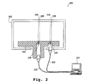
図2は、本発明の別の実施形態に従って、プロセスチャンバシステム200を示す図である。プロセスチャンバ202は、基板支持204を備えており、基板支持204は、複数の空洞206および216を有する。複数の空洞206および216の各々は、複数の材料208および218の各々を内部に保持するよう適切に構成されている。複数の透明カバー210および220の各々は、複数の空洞206および216の開口部をそれぞれ覆うよう適切に構成されている。したがって、各材料208および218は、それぞれ、複数の空洞208および218の1つに収容されており、材料208および218は、それぞれ、実質的に密封および隔離されている。透明カバー210および220は、プロセスチャンバシステム200内のプロセス条件に耐えるだけの耐性を備えた材料から形成される。かかる耐性を有する材料の一例として、石英が挙げられる。
FIG. 2 is a diagram illustrating a
図2に示すように、1または複数のセンサ212および222が、材料208および218の各々の相変化を監視するために、プロセスチャンバシステム200内に構成されている。1または複数のセンサ212および222によって収集された相変化データは、監視システム214に送信される。監視システム214は、システム制御部を備える。システム制御部は、プロセスチャンバ202のプロセス動作を含めて、プロセスチャンバシステム200の構成要素すべてを制御する。例えば、システム制御部は、プロセスチャンバ202内に投入されるプロセス薬剤の動作、基板を処理するためにプロセスチャンバ202内の表面を加熱する1または複数のヒータ、プロセスを開始するためにプロセスチャンバ202内の薬剤を活性化するエネルギ(例えば、RF、マイクロ波など)など、を制御してよい。監視システム214は、例えば、データ処理アルゴリズムを用いて、データを処理し、ユーザインターフェース(例えば、スクリーンモニタ)によって、解析データをユーザに対して適切に提示する。
As shown in FIG. 2, one or
図2において、1または複数のセンサ212および222は、材料208および218の相変化を監視し、各材料に相変化が起きると、相変化データを記録する。材料の相変化(例えば、固相から液相への変化)に対応する温度は、所与の圧力における特定の組成の材料については一定である。したがって、既知の組成の材料についての相変化の温度を、プロセスチャンバ202内のプロセス温度(例えば、基板支持204の表面温度)を測定するための基準として用いることができる。
In FIG. 2, one or
図3は、本発明の別の実施形態に従って、プロセスチャンバシステム300を示す図である。プロセスチャンバ302は、基板支持304と、チャンバ302の壁に組み込まれた複数の空洞336,346,356および366とを備える。複数の材料338,348,358および368が、それぞれ、チャンバ302の壁の中の複数の空洞336,346,356および366に収容されている。複数の空洞336,346,356および366の各々は、それぞれ、複数の透明カバー340,350,360および370によって密封されている。1または複数のセンサ312が、複数の透明カバー340,350,360および370を通して、複数の材料338,348,358および368の各々の相変化を検知するよう構成されている。図3には、1つのセンサ312が示されているが、各材料308,318,328,338,348,358および368の相変化を検知するために、1または複数のセンサ312が、プロセスチャンバ302内に構成されてよい。一実施形態では、センサ312は、レーザ分光計であってよい。センサ312は、プロセスチャンバシステムの制御部と通信するように接続される。センサ312は、材料308,318,328,338,348,358および368を監視して収集したデータを、データ処理のために、プロセスチャンバシステムの制御部に送信する。プロセスチャンバの制御部は、データ処理アルゴリズムを用いて、データを処理し、材料308,318,328,338,348,358および368の相変化温度に対応する光学定数の値を生成する。相変化温度は、さらに、処理されて、ユーザインターフェース(例えば、スクリーンモニタ)によってユーザに提示されてよい。ユーザに提示される情報は、温度分布のグラフ、例えば、時間に対する温度分布、位置に対する温度分布のグラフであってよい。
FIG. 3 is a diagram illustrating a
図4は、本発明の一実施形態に従って、プロセスチャンバシステム400を示す断面図である。プロセスチャンバシステム400においては、基板支持404が、プロセスチャンバ402内に配置されている。基板支持404上には、温度検知試験用基板415が配置される。温度検知試験用基板415は、基板層414と、透明カバー410とで構成される。複数の空洞406,426および436が、透明カバー410内に構成されており、複数の材料408,428および438が、それぞれ、複数の空洞406,426および436内に配置されている。材料408,428および438は、基板層414と接触している。透明層410は、プロセスチャンバ402の内部環境に対して、材料408,428および438を密閉しており、それにより、材料408,428および438が、プロセスチャンバ402の内部環境に汚染物質を導入しないようになっている。1または複数のセンサ412が、材料408,428および438の相変化を検知するために、プロセスチャンバ402内に構成されている。
FIG. 4 is a cross-sectional view illustrating a
図5は、本発明の一実施形態に従って、温度検知試験用基板415を示す拡大断面図である。温度検知試験用基板415は、基板層414と、透明カバー410とで構成される。透明カバー410は、複数の空洞406,426および436を備えるよう構成される。空洞406,426および436の各々は、複数の408,428および438の内の1つを収容する。材料408,428および438は、基板層414と接触しており、その結果、熱平衡の状態では、各材料408,428および438の温度が、各接触面の領域における基板層414の温度と同じになる。
FIG. 5 is an enlarged cross-sectional view illustrating a temperature
再び図4を参照して、プロセスチャンバ402でプロセスが開始されると、基板支持404は、通例は加熱される。温度検知試験用基板415は、プロセスチャンバ402内で処理されている基板の温度または熱の分布を決定するために用いられてよい。
Referring again to FIG. 4, when the process is initiated in the
十分な量の熱エネルギが、ヒータから基板支持404に伝導されると、温度検知試験用基板415の基板層414も、伝導および対流によって加熱される。基板層414は、プロセスチャンバ402内で処理されている実際の基板をシミュレートする。したがって、基板層414の温度は、プロセスチャンバ402内で処理されている基板の温度と同じである。基板層414と接触する材料408,428および438は、基板層414と同じ温度を有する。十分な熱エネルギが、材料408,428および438に伝導されると、材料の相変化が始まる。1または複数のセンサ412は、材料408,428および438の相変化を検知する。1または複数のセンサ412は、検知したデータを、データ処理のためにプロセスチャンバシステムの制御部に送信し、処理後のデータを、ユーザインターフェース(例えば、スクリーンモニタ)によってユーザに提示する。ユーザに提示される処理後のデータは、基板層414の温度分布のグラフの形態であってよく、それは、処理される基板の温度分布を表す。
When a sufficient amount of thermal energy is conducted from the heater to the
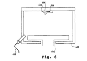
図6は、本発明の一実施形態に従って、温度検知要素を示す図である。温度検知要素610は、プロセスチャンバ602内に配置されている。温度検知要素は、材料608を収容するよう構成された透明シェル606を備える。透明シェル606は、材料の特性を損なうことなく、プロセスチャンバ602内の条件(例えば、熱、圧力、RFエネルギ、マイクロ波、反応性プラズマなど)に耐えることのできる耐性を有する材料から形成される。かかる耐性を有する材料の一例として、石英が挙げられる。材料608は、プロセスチャンバ602内の任意の表面と接触しつつ、プロセスチャンバ602内の接触面と透明シェル606との間に密封されるよう構成されている。センサ612が、透明シェル606を通して材料の相変化を検知するために、プロセスチャンバ602内に配置されている。例えば、センサ612は、レーザ分光計であってよい。材料608は、非常に正確な融点(例えば、0.1または0.2℃の範囲内の融点)を有する有機または無機化合物であってよい。これらの有機および無機化合物としては、ナフタレン、サリチル酸、ベンゾフェノン、硝酸コバルト(II)、安息香酸アルミニウム、酢酸アルミニウム、臭化アンチモン(III)および塩化アンチモン(III)が挙げられる。図および説明の簡単のために、図6では、プロセスチャンバ602に、温度検知要素610およびセンサ612を1つずつ配置した構成を示したが、本発明の範囲内で、任意の数の温度検知要素およびセンサを、プロセスチャンバ602に備えることができる。
FIG. 6 is a diagram illustrating a temperature sensing element according to one embodiment of the present invention. The
プロセスチャンバ602内でプロセスが開始されると、チャンバの表面も加熱されてよい。チャンバの表面は、多くの異なる方法で加熱される。チャンバの表面は、循環する流体、ヒータ、または、任意の他の適切な手段によって加熱されてよい。本発明の実施形態は、その場でのプロセス温度を正確に測定するための方法および装置を提供する。
As the process is initiated in
プロセスチャンバ602内の表面に接触する材料608は、接触面と同じ温度になる。十分な量の熱エネルギが、接触面から材料608に伝導されると、材料608で相変化が起きる。センサ612は、相変化を検知して、相変化データをプロセスチャンバシステムの制御部に送信する。プロセスチャンバシステムの制御部は、相変化データを処理して、処理後の相変化データをユーザインターフェース(例えば、スクリーンモニタ)によってユーザに提示する。処理後の相変化データは、温度分布グラフの形態であってよい。
The
図7Aは、本発明の一実施形態に従って、別の温度検知要素を示す図である。温度検知要素710は、プロセスチャンバ702内の基板支持704の上に配置されている。基板714も、基板支持704の上に配置される。温度検知要素710は、複数の空洞を有してよい。図7Aに示すように、温度検知要素710の空洞の内の2つには、それぞれ、材料718および728が収容されている。材料718および728は、基板支持704と接触している。センサ712および722は、材料718および728の相変化を検知するよう構成されている。図7Aには、材料718および728の相変化を検知するよう構成されたセンサ712および728が図示されているが、材料718および728の相変化を検知するために、任意の数のセンサを用いてよい。例えば、1つのセンサが、温度検知要素710に収容された任意の数の材料の相変化を検知するよう構成されてもよい。
FIG. 7A is a diagram illustrating another temperature sensing element, according to one embodiment of the present invention. The
図7Bは、温度検知要素710および基板714を示す上面図である。本発明の一実施形態に従った温度検知要素710は、温度検知と基板処理とを同時に行うことを可能にする。プロセスチャンバ702内でプロセスが開始されると、基板支持704は、通例、基板714の処理を促進するために加熱される。処理に向けて基板714を加熱するために、十分な量の熱エネルギが、ヒータから基板支持704に伝導されると、材料718,728,738および748も加熱される。材料718,728,738および748は、非常に正確な融点(例えば、0.1または0.2℃の範囲)を有するものが選択される。周知のように、材料の相変化に対応する温度は、特定の組成の材料については一定であるため、材料718,728,738および748の相変化を、基板714のプロセス温度を制御および監視するための基準温度として利用することができる。
FIG. 7B is a top view showing
プロセスの結果(例えば、半導体の素子形状の限界寸法)に影響する温度の変動を防ぐよう、プロセス温度(例えば、基板の表面温度)を制御するために、材料718,728,738および748の相変化を検知するよう構成されたセンサ712および722は、相変化データをプロセスチャンバシステムの制御部に送信する。さらに、プロセスチャンバシステムの制御部は、リアルタイムで処理後の相変化データをユーザインターフェース(例えば、スクリーンモニタ)によってユーザに提示できる。処理後の相変化データは、温度分布グラフの形態であってよい。
The phase of
図8は、本発明の一実施形態に従って、その場でのプロセス温度を正確に測定する方法を示すフローチャートである。その方法は、1または複数の温度検知要素をプロセスチャンバ内に配置する動作800から始まる。温度検知要素は、本発明の様々な実施形態に従って上述した温度検知要素のいずれであってもよい。次に、動作802において、プロセスチャンバ内でプロセスが開始される。開始されたプロセスは、最終的に、動作804において、それぞれの温度検知要素内の各材料の相変化を引き起こす。動作806において、プロセスチャンバ内の1または複数のセンサが、それぞれの温度検知要素内の材料の相変化を検出する。プロセスチャンバシステムの制御部は、動作808において、各材料の相変化データを処理する。動作810において、各材料の相変化に対応する温度が決定され、動作812において、それらの温度が記録される。本明細書で挙げた材料のいずれについても、相変化に対応する温度が、十分に立証されていることを理解されたい。例えば、ナフタレンは80.5℃の融点、サリチル酸は135℃の融点、ベンゾフェノンは48.1℃の融点、硝酸コバルト(II)は55℃の融点、安息香酸アルミニウムは198℃の融点、酢酸アルミニウムは114℃の融点、臭化アンチモン(III)は96.6℃の融点、塩化アンチモン(III)は73.4℃の融点を有する。
FIG. 8 is a flowchart illustrating a method for accurately measuring an in-situ process temperature in accordance with an embodiment of the present invention. The method begins with an
図9Aは、本発明の別の実施形態に従って、温度表示装置を示す図である。図9Aは、空洞906を有する温度表示装置904を示している。空洞906は、少なくとも2つの空間、例えば、第1の空間912と第2の空間914とを有する。この実施形態では、第1の空間912内に、材料908が配置される。カバー910が空洞906を密閉する。カバー910は、透明のカバーであってよく、それにより、上述のように、温度表示装置904を、その場でのプロセス温度を示すために利用できる。本発明の他の実施形態について上述した温度検知要素と同様に、温度表示装置904は、プロセスチャンバ内に配置されてよく、材料908の相変化は、カバー910を通して材料908の相変化を検知するよう構成されたセンサによって検知されてよい。
FIG. 9A is a diagram illustrating a temperature display device according to another embodiment of the present invention. FIG. 9A shows a
図9Bは、本発明の一実施形態に従って、材料908に位相変化が起きた状態の温度表示装置を示す図である。図9Bに示すように、材料908は、ある相から別の相(例えば、固相から液相、もしくは、液相から固相)に変化すると、第1の空間912から第2の空間914に移動される。温度表示装置904は、空洞906内の材料908の空間的な位置(すなわち、材料が、第1の空間912に収容されているか第2の空間914に収容されているか)を観察することによって、材料908に対応する位相変化温度に達したか否かを示すことができる。したがって、プロセスサイクルの終了後に、温度表示装置904を観察すれば、プロセスレシピが実行された時に、プロセス温度が、ある時点で材料908の相変化に対応する温度に到達したことを確認することができる。本発明の一実施形態では、カバー910は、透明カバーでなくてもよい。例えば、温度表示装置が、空間的な指標として利用される場合には、透明カバーを備える必要がない。
FIG. 9B is a diagram illustrating a temperature display device with a phase change in
本明細書では、本発明のいくつかの実施形態について詳細に説明したが、本発明の趣旨や範囲を逸脱することなく、様々な他の具体的な形態で本発明を実施できることは、当業者にとって明らかである。したがって、上述した例および実施形態は、例示に過ぎず、限定の意図はないため、本発明は、本明細書に記載した詳細事項には限定されず、添付した特許請求の範囲内で変型および実施することができる。 Although several embodiments of the invention have been described in detail herein, those skilled in the art will recognize that the invention can be implemented in various other specific forms without departing from the spirit or scope of the invention. It is obvious to Accordingly, the foregoing examples and embodiments are illustrative only and are not intended to be limiting, so the invention is not limited to the details described herein, and variations and modifications may be made within the scope of the appended claims. Can be implemented.
Claims (20)
前記プロセスチャンバ内に配置され、空洞を有する温度検知要素と、
前記空洞の開口部を覆うよう配置された透明カバーと、
前記温度検知要素の前記空洞内に配置された材料と、
前記透明カバーを通して、前記材料の相変化を検知するよう構成されたセンサと
を備えるプロセスチャンバ。 A process chamber,
A temperature sensing element disposed within the process chamber and having a cavity;
A transparent cover arranged to cover the opening of the cavity;
A material disposed within the cavity of the temperature sensing element;
And a sensor configured to sense a phase change of the material through the transparent cover.
前記有機化合物は、ナフタレン、サリチル酸、および、ベンゾフェノンの中から選択され、
前記無機化合物は、硝酸コバルト(II)、安息香酸アルミニウム、酢酸アルミニウム、臭化アンチモン(III)、および、塩化アンチモン(III)の中から選択された
プロセスチャンバ。 A process chamber according to claim 3, comprising:
The organic compound is selected from naphthalene, salicylic acid, and benzophenone,
The inorganic compound is a process chamber selected from cobalt (II) nitrate, aluminum benzoate, aluminum acetate, antimony (III) bromide, and antimony (III) chloride.
前記空洞は、少なくとも2つの空間を有し、
前記空洞内の前記材料は、前記材料の前記相変化が起きると、第1の空間から第2の空間に移動される
プロセスチャンバ。 The process chamber of claim 1, comprising:
The cavity has at least two spaces;
The material in the cavity is moved from a first space to a second space when the phase change of the material occurs.
表面の上に配置され、空洞を有し、透明な材料で形成された温度検知要素と、
前記温度検知要素の前記空洞内に配置され、前記表面と接触する材料と、
前記材料の相変化を検知するよう構成されたセンサと
を備えるプロセスチャンバ。 A process chamber,
A temperature sensing element disposed on the surface, having a cavity and formed of a transparent material;
A material disposed in the cavity of the temperature sensing element and in contact with the surface;
A process chamber comprising: a sensor configured to detect a phase change of the material.
埋め込まれた材料を有する温度検知要素を前記プロセスチャンバ内に配置する工程と、
前記プロセスチャンバ内でプロセス動作を開始する工程と、
前記埋め込まれた材料の相変化を検出する工程と、
前記相変化に対応する温度を記録する工程と
を備える方法。 A method for characterizing a temperature distribution in a process chamber, comprising:
Placing a temperature sensing element having an embedded material in the process chamber;
Initiating a process operation in the process chamber;
Detecting a phase change of the embedded material;
Recording a temperature corresponding to the phase change.
前記プロセスチャンバの内面上に前記温度検知要素を配置する工程を備える方法。 The method of claim 16, further comprising:
Disposing the temperature sensing element on an inner surface of the process chamber.
前記埋め込まれた材料を透明カバーで覆う工程を備える方法。 The method of claim 16, further comprising:
Covering the embedded material with a transparent cover.
Applications Claiming Priority (2)
| Application Number | Priority Date | Filing Date | Title |
|---|---|---|---|
| US11/097,063 | 2005-04-01 | ||
| US11/097,063 US7380982B2 (en) | 2005-04-01 | 2005-04-01 | Accurate temperature measurement for semiconductor applications |
Related Parent Applications (1)
| Application Number | Title | Priority Date | Filing Date |
|---|---|---|---|
| JP2008504129A Division JP5101490B2 (en) | 2005-04-01 | 2006-03-17 | Accurate temperature measurement in semiconductor applications |
Publications (2)
| Publication Number | Publication Date |
|---|---|
| JP2012094875A true JP2012094875A (en) | 2012-05-17 |
| JP5838079B2 JP5838079B2 (en) | 2015-12-24 |
Family
ID=37073932
Family Applications (2)
| Application Number | Title | Priority Date | Filing Date |
|---|---|---|---|
| JP2008504129A Expired - Fee Related JP5101490B2 (en) | 2005-04-01 | 2006-03-17 | Accurate temperature measurement in semiconductor applications |
| JP2011251423A Expired - Fee Related JP5838079B2 (en) | 2005-04-01 | 2011-11-17 | Accurate temperature measurement in semiconductor applications |
Family Applications Before (1)
| Application Number | Title | Priority Date | Filing Date |
|---|---|---|---|
| JP2008504129A Expired - Fee Related JP5101490B2 (en) | 2005-04-01 | 2006-03-17 | Accurate temperature measurement in semiconductor applications |
Country Status (6)
| Country | Link |
|---|---|
| US (1) | US7380982B2 (en) |
| JP (2) | JP5101490B2 (en) |
| KR (1) | KR101034169B1 (en) |
| CN (1) | CN101156056B (en) |
| TW (1) | TWI310961B (en) |
| WO (1) | WO2006107571A2 (en) |
Cited By (1)
| Publication number | Priority date | Publication date | Assignee | Title |
|---|---|---|---|---|
| WO2022163806A1 (en) * | 2021-02-01 | 2022-08-04 | 株式会社アルバック | Temperature measurement method, temperature measurement device, and thin film formation method |
Families Citing this family (13)
| Publication number | Priority date | Publication date | Assignee | Title |
|---|---|---|---|---|
| US7795605B2 (en) | 2007-06-29 | 2010-09-14 | International Business Machines Corporation | Phase change material based temperature sensor |
| US8388223B2 (en) * | 2007-08-09 | 2013-03-05 | The Edward Orton Jr. Ceramic Foundation | Furnace temperature monitoring device and method |
| KR101514098B1 (en) * | 2009-02-02 | 2015-04-21 | 도쿄엘렉트론가부시키가이샤 | Plasma processing apparatus and temperature measuring method and apparatus used therein |
| US9297705B2 (en) * | 2009-05-06 | 2016-03-29 | Asm America, Inc. | Smart temperature measuring device |
| US8911145B2 (en) * | 2009-11-20 | 2014-12-16 | The United States Of America As Represented By The Secretary Of The Navy | Method to measure the characteristics in an electrical component |
| CN102313599B (en) * | 2010-06-29 | 2013-04-24 | 北京北方微电子基地设备工艺研究中心有限责任公司 | Device and method for measuring temperature of coupling window, and plasma equipment |
| CN104296889B (en) * | 2013-07-16 | 2017-09-29 | 泰科电子(上海)有限公司 | Temperature indicator and the article for being provided with the temperature indicator |
| JP5769835B2 (en) * | 2014-02-14 | 2015-08-26 | 日油技研工業株式会社 | High temperature irreversible temperature control material |
| US9851263B2 (en) | 2015-09-29 | 2017-12-26 | Stephen Bugglin | Portable heating chamber system for pyrometric proficiency testing |
| WO2017132222A1 (en) * | 2016-01-25 | 2017-08-03 | Klt Technologies | Visual and electronically readable temperature indicator |
| US10736180B2 (en) * | 2017-04-28 | 2020-08-04 | Tutco Llc | Heater with an optical sensor for over-temperature protection |
| US10345159B1 (en) | 2018-03-20 | 2019-07-09 | Klt Technology, Inc. | Visual and electronically readable temperature indicator |
| CN111928967A (en) * | 2020-07-27 | 2020-11-13 | 北京航空航天大学 | Inside temperature measuring device of alkali metal air chamber |
Citations (4)
| Publication number | Priority date | Publication date | Assignee | Title |
|---|---|---|---|---|
| JPH01116421A (en) * | 1987-09-30 | 1989-05-09 | Walter Holzer | Method and apparatus for monitoring temperature for refrigerated and frozen goods |
| JP2003065862A (en) * | 2001-08-30 | 2003-03-05 | Kuromikku:Kk | Temperature display |
| JP2003515118A (en) * | 1999-11-18 | 2003-04-22 | センズアレイ コーポレイション | Optical technology for measuring parameters such as surface temperature |
| JP2004273470A (en) * | 2000-10-31 | 2004-09-30 | Tokyo Electron Ltd | Multi-component metal oxide thin film forming apparatus and method |
Family Cites Families (19)
| Publication number | Priority date | Publication date | Assignee | Title |
|---|---|---|---|---|
| US2261473A (en) * | 1938-04-16 | 1941-11-04 | George W Jennings | Temperature indicator |
| US4353990A (en) * | 1981-02-09 | 1982-10-12 | Minnesota Mining And Manufacturing Company | Sanitation indicator |
| GB8614839D0 (en) * | 1986-06-18 | 1986-07-23 | Gen Electric Co Plc | Indicating changes in temperatures |
| US5159564A (en) * | 1988-12-22 | 1992-10-27 | North Carolina State University | Thermal memory cell and thermal system evaluation |
| US5310260A (en) * | 1990-04-10 | 1994-05-10 | Luxtron Corporation | Non-contact optical techniques for measuring surface conditions |
| US5118200A (en) * | 1990-06-13 | 1992-06-02 | Varian Associates, Inc. | Method and apparatus for temperature measurements |
| US5158364A (en) * | 1990-12-21 | 1992-10-27 | Temple University | Method of making and using an improved liquid crystal cumulative dosimeter container |
| US5377126A (en) * | 1991-09-13 | 1994-12-27 | Massachusetts Institute Of Technology | Non-contact temperature measurement of a film growing on a substrate |
| US5215378A (en) * | 1992-04-17 | 1993-06-01 | Introtech, Inc. | Dual temperature indicator |
| US5313044A (en) * | 1992-04-28 | 1994-05-17 | Duke University | Method and apparatus for real-time wafer temperature and thin film growth measurement and control in a lamp-heated rapid thermal processor |
| US5265957A (en) * | 1992-08-11 | 1993-11-30 | Texas Instruments Incorporated | Wireless temperature calibration device and method |
| JP3407749B2 (en) * | 1992-09-03 | 2003-05-19 | 富士電機株式会社 | Induction furnace shelves protection device |
| US5641707A (en) * | 1994-10-31 | 1997-06-24 | Texas Instruments Incorporated | Direct gas-phase doping of semiconductor wafers using an organic dopant source of phosphorus |
| EP1101085B1 (en) * | 1998-07-28 | 2002-10-09 | STEAG RTP Systems GmbH | Method and device for calibrating measurements of temperatures independent of emissivity |
| US6479801B1 (en) * | 1999-10-22 | 2002-11-12 | Tokyo Electron Limited | Temperature measuring method, temperature control method and processing apparatus |
| US7080940B2 (en) * | 2001-04-20 | 2006-07-25 | Luxtron Corporation | In situ optical surface temperature measuring techniques and devices |
| US6572265B1 (en) * | 2001-04-20 | 2003-06-03 | Luxtron Corporation | In situ optical surface temperature measuring techniques and devices |
| US6786637B2 (en) * | 2002-09-13 | 2004-09-07 | The University Of Bristol | Temperature measurement of an electronic device |
| DE10307933B3 (en) * | 2003-02-25 | 2004-06-03 | Ivoclar Vivadent Ag | Calibration device for dental oven temperature using metallic melting element with defined melting temperature and device providing indication of its melting |
-
2005
- 2005-04-01 US US11/097,063 patent/US7380982B2/en not_active Expired - Fee Related
-
2006
- 2006-03-17 KR KR1020077025446A patent/KR101034169B1/en not_active Expired - Fee Related
- 2006-03-17 JP JP2008504129A patent/JP5101490B2/en not_active Expired - Fee Related
- 2006-03-17 CN CN2006800110594A patent/CN101156056B/en not_active Expired - Fee Related
- 2006-03-17 WO PCT/US2006/009879 patent/WO2006107571A2/en not_active Ceased
- 2006-03-31 TW TW095111411A patent/TWI310961B/en not_active IP Right Cessation
-
2011
- 2011-11-17 JP JP2011251423A patent/JP5838079B2/en not_active Expired - Fee Related
Patent Citations (4)
| Publication number | Priority date | Publication date | Assignee | Title |
|---|---|---|---|---|
| JPH01116421A (en) * | 1987-09-30 | 1989-05-09 | Walter Holzer | Method and apparatus for monitoring temperature for refrigerated and frozen goods |
| JP2003515118A (en) * | 1999-11-18 | 2003-04-22 | センズアレイ コーポレイション | Optical technology for measuring parameters such as surface temperature |
| JP2004273470A (en) * | 2000-10-31 | 2004-09-30 | Tokyo Electron Ltd | Multi-component metal oxide thin film forming apparatus and method |
| JP2003065862A (en) * | 2001-08-30 | 2003-03-05 | Kuromikku:Kk | Temperature display |
Cited By (1)
| Publication number | Priority date | Publication date | Assignee | Title |
|---|---|---|---|---|
| WO2022163806A1 (en) * | 2021-02-01 | 2022-08-04 | 株式会社アルバック | Temperature measurement method, temperature measurement device, and thin film formation method |
Also Published As
| Publication number | Publication date |
|---|---|
| KR20080004566A (en) | 2008-01-09 |
| TW200707510A (en) | 2007-02-16 |
| TWI310961B (en) | 2009-06-11 |
| WO2006107571A3 (en) | 2007-03-01 |
| KR101034169B1 (en) | 2011-05-12 |
| JP2008534961A (en) | 2008-08-28 |
| JP5101490B2 (en) | 2012-12-19 |
| CN101156056A (en) | 2008-04-02 |
| WO2006107571A2 (en) | 2006-10-12 |
| CN101156056B (en) | 2013-12-11 |
| JP5838079B2 (en) | 2015-12-24 |
| US7380982B2 (en) | 2008-06-03 |
| US20080025370A1 (en) | 2008-01-31 |
Similar Documents
| Publication | Publication Date | Title |
|---|---|---|
| JP5838079B2 (en) | Accurate temperature measurement in semiconductor applications | |
| KR101813308B1 (en) | Process condition measuring device (pcmd) and method for measuring process conditions in a workpiece processing tool configured to process production workpieces | |
| JP6537329B2 (en) | Temperature control device, temperature control method and program | |
| JP7171765B2 (en) | Fiber optic probe with dual sealing and compression element | |
| WO2006070689A1 (en) | Semiconductor manufacturing apparatus, abnormality detection in such semiconductor manufacturing apparatus, method for specifying abnormality cause or predicting abnormality, and recording medium wherein computer program for executing such method is recorded | |
| US20070055403A1 (en) | Methods of and apparatuses for maintenance, diagnosis, and optimization of processes | |
| US20080224817A1 (en) | Interlaced rtd sensor for zone/average temperature sensing | |
| KR20130032254A (en) | Method and apparatus for depositing a layer on a semiconductor wafer by vapor deposition in a process chamber | |
| KR100882633B1 (en) | Computer-readable recording media recording heat treatment apparatus, heat treatment method, control apparatus and program | |
| JP2006186280A (en) | Semiconductor manufacturing apparatus and storage medium | |
| US10607869B2 (en) | Substrate processing system and control device | |
| JP5554518B2 (en) | Method and apparatus for determining substrate temperature | |
| JP4998333B2 (en) | Temperature measuring device, mounting table structure, and heat treatment device | |
| TWI767326B (en) | Substrate processing device, manufacturing method of semiconductor device, and warning detection program | |
| KR100503515B1 (en) | Apparatus of temperature calibration and method of temperature calibration using the same | |
| CN223373209U (en) | Substrate processing apparatus and substrate temperature measuring assembly | |
| JP2004071794A (en) | Substrate processing equipment | |
| JP2008141071A (en) | Substrate heat treatment equipment | |
| JP4213133B2 (en) | Manufacturing method of processing apparatus, manufacturing method of quartz product in processing apparatus, and measuring jig | |
| Moelders et al. | Localized, in-situ vacuum measurements for MEMS packaging | |
| KR20060134690A (en) | Semiconductor equipment with chuck | |
| JPH0563054A (en) | Wafer temperature measuring method and apparatus | |
| KR20250020316A (en) | Information processing apparatus, substrate processing apparatus, and information processing method | |
| TW202303104A (en) | Mitigating thermal expansion mismatch in temperature probe construction apparatus and method | |
| Wang et al. | Plasma etch process diagnosis and control by wireless sensor wafer in semiconductor chip manufacturing |
Legal Events
| Date | Code | Title | Description |
|---|---|---|---|
| A977 | Report on retrieval |
Free format text: JAPANESE INTERMEDIATE CODE: A971007 Effective date: 20130415 |
|
| A131 | Notification of reasons for refusal |
Free format text: JAPANESE INTERMEDIATE CODE: A131 Effective date: 20130423 |
|
| A601 | Written request for extension of time |
Free format text: JAPANESE INTERMEDIATE CODE: A601 Effective date: 20130722 |
|
| A602 | Written permission of extension of time |
Free format text: JAPANESE INTERMEDIATE CODE: A602 Effective date: 20130725 |
|
| A521 | Request for written amendment filed |
Free format text: JAPANESE INTERMEDIATE CODE: A523 Effective date: 20131022 |
|
| A02 | Decision of refusal |
Free format text: JAPANESE INTERMEDIATE CODE: A02 Effective date: 20140225 |
|
| A521 | Request for written amendment filed |
Free format text: JAPANESE INTERMEDIATE CODE: A821 Effective date: 20140625 |
|
| A601 | Written request for extension of time |
Free format text: JAPANESE INTERMEDIATE CODE: A601 Effective date: 20150818 |
|
| A521 | Request for written amendment filed |
Free format text: JAPANESE INTERMEDIATE CODE: A523 Effective date: 20150918 |
|
| A61 | First payment of annual fees (during grant procedure) |
Free format text: JAPANESE INTERMEDIATE CODE: A61 Effective date: 20151109 |
|
| R150 | Certificate of patent or registration of utility model |
Ref document number: 5838079 Country of ref document: JP Free format text: JAPANESE INTERMEDIATE CODE: R150 |
|
| R250 | Receipt of annual fees |
Free format text: JAPANESE INTERMEDIATE CODE: R250 |
|
| R250 | Receipt of annual fees |
Free format text: JAPANESE INTERMEDIATE CODE: R250 |
|
| LAPS | Cancellation because of no payment of annual fees |