JP2012104538A - 半導体発光装置 - Google Patents
半導体発光装置 Download PDFInfo
- Publication number
- JP2012104538A JP2012104538A JP2010249549A JP2010249549A JP2012104538A JP 2012104538 A JP2012104538 A JP 2012104538A JP 2010249549 A JP2010249549 A JP 2010249549A JP 2010249549 A JP2010249549 A JP 2010249549A JP 2012104538 A JP2012104538 A JP 2012104538A
- Authority
- JP
- Japan
- Prior art keywords
- semiconductor light
- light emitting
- led
- emitting device
- conductor wiring
- Prior art date
- Legal status (The legal status is an assumption and is not a legal conclusion. Google has not performed a legal analysis and makes no representation as to the accuracy of the status listed.)
- Granted
Links
Images


Classifications
-
- H—ELECTRICITY
- H10—SEMICONDUCTOR DEVICES; ELECTRIC SOLID-STATE DEVICES NOT OTHERWISE PROVIDED FOR
- H10W—GENERIC PACKAGES, INTERCONNECTIONS, CONNECTORS OR OTHER CONSTRUCTIONAL DETAILS OF DEVICES COVERED BY CLASS H10
- H10W72/00—Interconnections or connectors in packages
- H10W72/071—Connecting or disconnecting
- H10W72/073—Connecting or disconnecting of die-attach connectors
-
- H—ELECTRICITY
- H10—SEMICONDUCTOR DEVICES; ELECTRIC SOLID-STATE DEVICES NOT OTHERWISE PROVIDED FOR
- H10W—GENERIC PACKAGES, INTERCONNECTIONS, CONNECTORS OR OTHER CONSTRUCTIONAL DETAILS OF DEVICES COVERED BY CLASS H10
- H10W72/00—Interconnections or connectors in packages
- H10W72/071—Connecting or disconnecting
- H10W72/075—Connecting or disconnecting of bond wires
-
- H—ELECTRICITY
- H10—SEMICONDUCTOR DEVICES; ELECTRIC SOLID-STATE DEVICES NOT OTHERWISE PROVIDED FOR
- H10W—GENERIC PACKAGES, INTERCONNECTIONS, CONNECTORS OR OTHER CONSTRUCTIONAL DETAILS OF DEVICES COVERED BY CLASS H10
- H10W72/00—Interconnections or connectors in packages
- H10W72/851—Dispositions of multiple connectors or interconnections
- H10W72/874—On different surfaces
- H10W72/884—Die-attach connectors and bond wires
Landscapes
- Led Device Packages (AREA)
- Led Devices (AREA)
Abstract
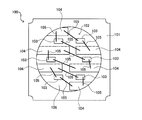
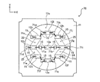
【解決手段】拡散反射面を形成する素子搭載面と、前記素子搭載面上に設けられた導体配線と、を有する基板と、それぞれが長方形の外形を有し、前記素子搭載面上に搭載方向が同一となるように環状に配列され且つ前記導体配線に電気的に接続された複数の半導体発光素子と、を含み、前記導体配線は、互いに隣接する2つの半導体発光素子間の対向する長辺の一端及び他端同士を結ぶ線分と前記2つの半導体発光素子の対向する長辺とによって囲まれた素子間領域内に侵入していないこと。
【選択図】図2
Description
11 基板
11a 第1セラミック層
11b 第2セラミック層
12a〜12i 発光ダイオード(LED)
13 透光性樹脂
14a〜14j 導体配線
15 ボンディングワイヤ
16 接着剤
21 環状領域(素子搭載領域)
22〜25 素子間領域
Claims (4)
- 拡散反射面を形成する素子搭載面と、前記素子搭載面上に設けられた導体配線と、を有する基板と、
それぞれが長方形の外形を有し、前記素子搭載面上に搭載方向が同一となるように環状に配列され且つ前記導体配線に電気的に接続された複数の半導体発光素子と、を含み、
前記導体配線は、互いに隣接する2つの半導体発光素子間の対向する長辺の一端及び他端同士を結ぶ線分と前記2つの半導体発光素子の対向する長辺とによって囲まれた素子間領域内に侵入していないことを特徴とする半導体発光装置。 - 前記導体配線は、前記複数の半導体発光素子に囲まれた領域内において細長形状に配置され、長手方向が前記半導体発光素子の長辺方向に略垂直であることを特徴とする請求項1に記載の半導体発光装置。
- 前記基板は前記拡散反射面上に複数の溝を有し、前記複数の溝の底部に前記複数の導体配線が設けられていることを特徴とする請求項1又は2に記載の半導体発光装置。
- 前記溝は白色樹脂によって充填されていることを特徴とする請求項3記載の半導体発光装置。
Priority Applications (1)
| Application Number | Priority Date | Filing Date | Title |
|---|---|---|---|
| JP2010249549A JP5669525B2 (ja) | 2010-11-08 | 2010-11-08 | 半導体発光装置 |
Applications Claiming Priority (1)
| Application Number | Priority Date | Filing Date | Title |
|---|---|---|---|
| JP2010249549A JP5669525B2 (ja) | 2010-11-08 | 2010-11-08 | 半導体発光装置 |
Publications (2)
| Publication Number | Publication Date |
|---|---|
| JP2012104538A true JP2012104538A (ja) | 2012-05-31 |
| JP5669525B2 JP5669525B2 (ja) | 2015-02-12 |
Family
ID=46394632
Family Applications (1)
| Application Number | Title | Priority Date | Filing Date |
|---|---|---|---|
| JP2010249549A Expired - Fee Related JP5669525B2 (ja) | 2010-11-08 | 2010-11-08 | 半導体発光装置 |
Country Status (1)
| Country | Link |
|---|---|
| JP (1) | JP5669525B2 (ja) |
Cited By (2)
| Publication number | Priority date | Publication date | Assignee | Title |
|---|---|---|---|---|
| JP2015008237A (ja) * | 2013-06-26 | 2015-01-15 | 日亜化学工業株式会社 | 発光装置 |
| US9202990B2 (en) | 2014-02-04 | 2015-12-01 | Samsung Display Co., Ltd. | Light emitting diode package and backlight unit including the same |
Citations (5)
| Publication number | Priority date | Publication date | Assignee | Title |
|---|---|---|---|---|
| JPS5183277U (ja) * | 1974-12-25 | 1976-07-03 | ||
| JP2009283776A (ja) * | 2008-05-23 | 2009-12-03 | Stanley Electric Co Ltd | 半導体装置、半導体装置モジュール及び半導体装置モジュールの製造方法 |
| JP2010147189A (ja) * | 2008-12-17 | 2010-07-01 | Panasonic Electric Works Co Ltd | 発光装置 |
| JP2010182878A (ja) * | 2009-02-05 | 2010-08-19 | Sumitomo Metal Electronics Devices Inc | 発光素子搭載用パッケージ |
| JP2010287583A (ja) * | 2009-06-09 | 2010-12-24 | Toyoda Gosei Co Ltd | Ledランプ |
-
2010
- 2010-11-08 JP JP2010249549A patent/JP5669525B2/ja not_active Expired - Fee Related
Patent Citations (5)
| Publication number | Priority date | Publication date | Assignee | Title |
|---|---|---|---|---|
| JPS5183277U (ja) * | 1974-12-25 | 1976-07-03 | ||
| JP2009283776A (ja) * | 2008-05-23 | 2009-12-03 | Stanley Electric Co Ltd | 半導体装置、半導体装置モジュール及び半導体装置モジュールの製造方法 |
| JP2010147189A (ja) * | 2008-12-17 | 2010-07-01 | Panasonic Electric Works Co Ltd | 発光装置 |
| JP2010182878A (ja) * | 2009-02-05 | 2010-08-19 | Sumitomo Metal Electronics Devices Inc | 発光素子搭載用パッケージ |
| JP2010287583A (ja) * | 2009-06-09 | 2010-12-24 | Toyoda Gosei Co Ltd | Ledランプ |
Cited By (2)
| Publication number | Priority date | Publication date | Assignee | Title |
|---|---|---|---|---|
| JP2015008237A (ja) * | 2013-06-26 | 2015-01-15 | 日亜化学工業株式会社 | 発光装置 |
| US9202990B2 (en) | 2014-02-04 | 2015-12-01 | Samsung Display Co., Ltd. | Light emitting diode package and backlight unit including the same |
Also Published As
| Publication number | Publication date |
|---|---|
| JP5669525B2 (ja) | 2015-02-12 |
Similar Documents
| Publication | Publication Date | Title |
|---|---|---|
| CN105702842B (zh) | 光电子半导体器件 | |
| US10749079B2 (en) | LED module | |
| EP2228841A1 (en) | LED module with improved light output | |
| US20100258825A1 (en) | Light emitting device | |
| JP2012181953A (ja) | 照明装置 | |
| JP2016062899A (ja) | 半導体発光装置 | |
| US11605765B2 (en) | LED module | |
| JP2017050445A (ja) | 発光装置、及び照明装置 | |
| JP2015079917A (ja) | 半導体発光装置 | |
| KR20100106224A (ko) | 반도체 발광장치 | |
| JP5669525B2 (ja) | 半導体発光装置 | |
| JP2018206886A (ja) | 発光装置、及び、照明装置 | |
| KR20130014755A (ko) | 발광 소자 패키지 및 조명 시스템 | |
| KR101827972B1 (ko) | 발광 패키지 및 그를 이용한 백라이트 모듈 | |
| JP2019016728A (ja) | 発光装置、照明装置、及び、実装基板 | |
| JP2007324204A (ja) | 発光装置 | |
| CN101630706A (zh) | 正向出光型发光二极管结构 | |
| JP7285439B2 (ja) | 面状光源 | |
| KR101125456B1 (ko) | 발광소자 및 그를 이용한 라이트 유닛 | |
| JP5955888B2 (ja) | 発光装置 | |
| JP6028443B2 (ja) | 発光装置 | |
| JP2019021742A (ja) | 発光装置、及び、照明装置 | |
| JP2009152525A (ja) | 発光装置および照明装置 | |
| KR101806789B1 (ko) | 반도체 발광소자 | |
| KR101363077B1 (ko) | 발광 장치 |
Legal Events
| Date | Code | Title | Description |
|---|---|---|---|
| A621 | Written request for application examination |
Free format text: JAPANESE INTERMEDIATE CODE: A621 Effective date: 20131007 |
|
| A977 | Report on retrieval |
Free format text: JAPANESE INTERMEDIATE CODE: A971007 Effective date: 20140319 |
|
| A131 | Notification of reasons for refusal |
Free format text: JAPANESE INTERMEDIATE CODE: A131 Effective date: 20140902 |
|
| A521 | Request for written amendment filed |
Free format text: JAPANESE INTERMEDIATE CODE: A523 Effective date: 20141031 |
|
| TRDD | Decision of grant or rejection written | ||
| A01 | Written decision to grant a patent or to grant a registration (utility model) |
Free format text: JAPANESE INTERMEDIATE CODE: A01 Effective date: 20141202 |
|
| A61 | First payment of annual fees (during grant procedure) |
Free format text: JAPANESE INTERMEDIATE CODE: A61 Effective date: 20141216 |
|
| R150 | Certificate of patent or registration of utility model |
Ref document number: 5669525 Country of ref document: JP Free format text: JAPANESE INTERMEDIATE CODE: R150 |
|
| R250 | Receipt of annual fees |
Free format text: JAPANESE INTERMEDIATE CODE: R250 |
|
| R250 | Receipt of annual fees |
Free format text: JAPANESE INTERMEDIATE CODE: R250 |
|
| R250 | Receipt of annual fees |
Free format text: JAPANESE INTERMEDIATE CODE: R250 |
|
| R250 | Receipt of annual fees |
Free format text: JAPANESE INTERMEDIATE CODE: R250 |
|
| R250 | Receipt of annual fees |
Free format text: JAPANESE INTERMEDIATE CODE: R250 |
|
| LAPS | Cancellation because of no payment of annual fees |