JP2012109263A - Manufacturing method of superconducting tape wire rod, superconducting tape wire rod, and superconducting apparatus - Google Patents
Manufacturing method of superconducting tape wire rod, superconducting tape wire rod, and superconducting apparatus Download PDFInfo
- Publication number
- JP2012109263A JP2012109263A JP2012024797A JP2012024797A JP2012109263A JP 2012109263 A JP2012109263 A JP 2012109263A JP 2012024797 A JP2012024797 A JP 2012024797A JP 2012024797 A JP2012024797 A JP 2012024797A JP 2012109263 A JP2012109263 A JP 2012109263A
- Authority
- JP
- Japan
- Prior art keywords
- superconducting
- layer
- tape
- region
- thin film
- Prior art date
- Legal status (The legal status is an assumption and is not a legal conclusion. Google has not performed a legal analysis and makes no representation as to the accuracy of the status listed.)
- Pending
Links
Images




Classifications
-
- Y—GENERAL TAGGING OF NEW TECHNOLOGICAL DEVELOPMENTS; GENERAL TAGGING OF CROSS-SECTIONAL TECHNOLOGIES SPANNING OVER SEVERAL SECTIONS OF THE IPC; TECHNICAL SUBJECTS COVERED BY FORMER USPC CROSS-REFERENCE ART COLLECTIONS [XRACs] AND DIGESTS
- Y02—TECHNOLOGIES OR APPLICATIONS FOR MITIGATION OR ADAPTATION AGAINST CLIMATE CHANGE
- Y02E—REDUCTION OF GREENHOUSE GAS [GHG] EMISSIONS, RELATED TO ENERGY GENERATION, TRANSMISSION OR DISTRIBUTION
- Y02E40/00—Technologies for an efficient electrical power generation, transmission or distribution
- Y02E40/60—Superconducting electric elements or equipment; Power systems integrating superconducting elements or equipment
Landscapes
- Inorganic Compounds Of Heavy Metals (AREA)
- Superconductors And Manufacturing Methods Therefor (AREA)
Abstract
【課題】長尺な線材と同様の効果を有する超電導テープ線材の製造方法、超電導テープ線材、および超電導機器を提供する。
【解決手段】超電導テープ線材30の製造方法は、テープ状基板31を準備する工程(S10)と、テープ状基板31上に中間薄膜層32を形成する工程(S20)と、中間薄膜層32は一方端部32cから他方端部32dまで伸び、中間薄膜層32に一方端部32cから他方端部32dまで延在する少なくとも1つの中間層分割領域32aを形成する工程(S50)と、中間薄膜層32上に超電導層33を形成する工程(S30)とを備えている。超伝導領域層33aは、超電導層33bの臨界温度では超電導状態とならない領域であることを特徴とする。
【選択図】図5A superconducting tape wire manufacturing method, a superconducting tape wire, and a superconducting device having the same effect as a long wire.
A method of manufacturing a superconducting tape wire 30 includes a step of preparing a tape-like substrate 31 (S10), a step of forming an intermediate thin film layer 32 on the tape-like substrate 31 (S20), and an intermediate thin film layer 32 comprising: A step (S50) of forming at least one intermediate layer division region 32a extending from one end 32c to the other end 32d and extending from the one end 32c to the other end 32d in the intermediate thin film layer 32; And a step (S30) of forming a superconducting layer 33 on 32. The superconducting region layer 33a is a region that is not in a superconducting state at the critical temperature of the superconducting layer 33b.
[Selection] Figure 5
Description
本発明は、超電導テープ線材の製造方法、超電導テープ線材、および超電導機器に関する。 The present invention relates to a method for producing a superconducting tape wire, a superconducting tape wire, and a superconducting device.
従来、高磁界コイルにビスマス系高温超電導線材が用いられている。また、最近は、Y(イットリウム)系薄膜テープ高温超電導線材が用いられることもある。また、金属系超電導線材を用いて、周波数900MHz〜920MHzのNMRコイルを作製している。このようなNMRコイルを作製するためには、長尺で均一な線材が必要である。 Conventionally, bismuth-based high-temperature superconducting wires have been used for high-field coils. Recently, Y (yttrium) thin film tape high-temperature superconducting wires may be used. In addition, an NMR coil having a frequency of 900 MHz to 920 MHz is produced using a metallic superconducting wire. In order to produce such an NMR coil, a long and uniform wire is required.
長尺で均一な特性の線材の製造方法として、特開平6−120025号公報(特許文献1)では、酸化物超電導コイルの製造方法が開示されている。特許文献1には、コイルの中心軸に対してコイルの内径と外形とを結ぶ直線が中心軸に対して回転したときに、その直線と中心軸との交点が、中心軸の上下方向に移動するらせん状の連続面を有する非超電導体製基板を用意し、その基板上に酸化物超電導体を成膜する方法が開示されている。 As a method for producing a long and uniform wire, JP-A-6-120025 (Patent Document 1) discloses a method for producing an oxide superconducting coil. In Patent Document 1, when a straight line connecting the inner diameter and the outer shape of the coil with respect to the central axis of the coil rotates with respect to the central axis, the intersection of the straight line and the central axis moves in the vertical direction of the central axis. A method is disclosed in which a non-superconductor substrate having a helical continuous surface is prepared, and an oxide superconductor film is formed on the substrate.
しかしながら、周波数1GHzのNMRコイルを作製するためには、たとえばBi−2212組成のBi(ビスマス)系線材では、温度が4.2K、磁束密度が25T、Ic(臨界電流)=300Aの条件下で、内径1mmの丸線の場合、単長が1600mという長尺な線材が必要となる。また、Y系薄膜線材では、同様の条件下で、幅1cmのテープ線材の場合、単長が500m必要となる。そのため、超電導線材を用いてコイルを作製するためには、長尺で均一な特性の線材が必要となる。特に高磁界コイルを作製する際には、そのような線材が要求される。 However, in order to fabricate an NMR coil having a frequency of 1 GHz, for example, with a Bi-2212 composition Bi (bismuth) wire, the temperature is 4.2 K, the magnetic flux density is 25 T, and Ic (critical current) = 300 A. In the case of a round wire having an inner diameter of 1 mm, a long wire having a single length of 1600 m is required. In the case of a Y-based thin film wire, a single length of 500 m is required in the case of a tape wire having a width of 1 cm under the same conditions. Therefore, in order to produce a coil using a superconducting wire, a long and uniform wire is required. In particular, when producing a high magnetic field coil, such a wire is required.
しかし、上記超電導線材では、上述のような長尺の線材を作成することは困難である。また、上記のような長尺な線材を実現した場合であっても、製造するのに非常に高価なものとなるため、工業製品とすることは非常に困難であるという問題がある。 However, with the superconducting wire, it is difficult to produce a long wire as described above. Further, even when a long wire as described above is realized, there is a problem that it is very difficult to produce an industrial product because it is very expensive to manufacture.
また、上記特許文献1に記載の酸化物超電導コイルの製造方法では、らせん状の連続面を有する非超電導体製基板上に酸化物超電導体を成膜しているので、長尺な線材を製造することはできる。しかし、この場合も上述したように工業化が困難であるという問題がある。 Moreover, in the manufacturing method of the oxide superconducting coil described in Patent Document 1, an oxide superconductor is formed on a non-superconductor substrate having a spiral continuous surface, so that a long wire is manufactured. Can do. However, also in this case, there is a problem that industrialization is difficult as described above.
それゆえ本発明の目的は、上記のような課題を解決するためになされたものであり、長尺な線材と同様の効果を有する超電導テープ線材の製造方法、超電導テープ線材、および超電導機器を提供することである。 Therefore, an object of the present invention is to solve the above-described problems, and provides a method of manufacturing a superconducting tape wire, a superconducting tape wire, and a superconducting device having the same effect as a long wire. It is to be.
本発明の一の局面における超電導テープ線材の製造方法によれば、テープ状基板を準備する工程と、テープ状基板上に中間薄膜層を形成する工程と、中間薄膜層上に超電導層を形成する工程と、超電導層は一方端部から他方端部まで伸び、超電導層に一方端部から他方端部まで延在する少なくとも1つの分割領域を形成する加工工程とを備える。分割領域は、超電導層の臨界温度では超電導状態とならない領域であることを特徴とする。 According to the method for manufacturing a superconducting tape wire in one aspect of the present invention, a step of preparing a tape-shaped substrate, a step of forming an intermediate thin film layer on the tape-shaped substrate, and a superconducting layer formed on the intermediate thin film layer A superconducting layer extending from one end to the other end and forming at least one divided region extending from the one end to the other end in the superconducting layer. The divided region is a region that is not in a superconducting state at the critical temperature of the superconducting layer.
本発明の他の局面における超電導テープ線材の製造方法によれば、テープ状基板を準備する工程と、テープ状基板上に中間薄膜層を形成する工程と、中間薄膜層は一方端部から他方端部まで伸び、中間薄膜層に一方端部から他方端部まで延在する少なくとも1つの中間層分割領域を形成する加工工程と、中間薄膜層上に超電導層を形成する工程とを備える。中間層分割領域上の超電導層領域は、超電導層の臨界温度では超電導状態とならない領域であることを特徴とする。 According to the method of manufacturing a superconducting tape wire in another aspect of the present invention, a step of preparing a tape-shaped substrate, a step of forming an intermediate thin film layer on the tape-shaped substrate, and the intermediate thin film layer from one end to the other end And a processing step of forming at least one intermediate layer division region extending from one end to the other end of the intermediate thin film layer, and a step of forming a superconducting layer on the intermediate thin film layer. The superconducting layer region on the intermediate layer dividing region is a region that does not enter a superconducting state at the critical temperature of the superconducting layer.
本発明の一の局面における超電導テープ線材は、テープ状基板と、テープ状基板上に形成された中間薄膜層と、中間薄膜層上に形成され、一方端部から他方端部まで伸び、一方端部から他方端部まで延在する少なくとも1つの分割領域を含む超電導層とを備える。分割領域は、超電導層の臨界温度では超電導状態とならない領域であることを特徴とする。 A superconducting tape wire according to one aspect of the present invention is formed on a tape-shaped substrate, an intermediate thin film layer formed on the tape-shaped substrate, and the intermediate thin film layer, and extends from one end to the other end. And a superconducting layer including at least one divided region extending from the portion to the other end. The divided region is a region that is not in a superconducting state at the critical temperature of the superconducting layer.
本発明の他の局面における超電導テープ線材は、テープ状基板と、テープ状基板上に形成され、一方端部から他方端部まで伸び、一方端部から他方端部まで延在する少なくとも1つの分割領域を含む中間薄膜層と、中間薄膜層上に形成された超電導層とを備え、中間層分割領域上の超電導層領域は、超電導層の臨界温度では超電導状態とならない領域であることを特徴とする。 A superconducting tape wire according to another aspect of the present invention is formed on a tape-shaped substrate and the tape-shaped substrate, extends from one end to the other end, and extends from one end to the other end. An intermediate thin film layer including a region and a superconducting layer formed on the intermediate thin film layer, wherein the superconducting layer region on the intermediate layer dividing region is a region that does not enter a superconducting state at a critical temperature of the superconducting layer. To do.
本発明の超電導機器は、上記超電導テープ線材を用いている。 The superconducting device of the present invention uses the superconducting tape wire.
本発明の超電導テープ線材の製造方法によれば、加工工程により分割領域または中間層分割領域を形成する。そのため、幅広の超電導テープ線材を相対的に幅の狭い複数の並列に配置された、または1本の直列に配置された超電導テープ線材に加工することができる。このような並列に配置された複数の、または直列に配置された1本の超電導テープ線材を用いてたとえばコイルなどの機器を製造すれば、上記複数の超電導テープ線材を直列に接続したような長尺のテープ線材を使ってコイルを製造した場合と同様の巻き数のコイルを容易に製造できる。つまり、長尺な線材と同様の効果を有する超電導テープ線材を容易に製造することができる。 According to the method for manufacturing a superconducting tape wire of the present invention, a divided region or an intermediate layer divided region is formed by a processing step. Therefore, a wide superconducting tape wire can be processed into a plurality of relatively narrow superconducting tape wires arranged in parallel or one in series. If a device such as a coil is manufactured using a plurality of such superconducting tape wires arranged in parallel or a single superconducting tape wire arranged in series, such a length that the plurality of superconducting tape wires are connected in series. It is possible to easily manufacture a coil having the same number of turns as when a coil is manufactured using a long tape wire. That is, a superconducting tape wire having the same effect as that of a long wire can be easily manufactured.
本発明の超電導テープ線材によれば、分割領域または中間層分割領域を備えている。そのため、線材を並列に複数枚集めたものと同様の効果を有する幅広の超電導テープ線材とすることができる。 According to the superconducting tape wire of the present invention, it has a divided region or an intermediate layer divided region. Therefore, it is possible to obtain a wide superconducting tape wire having the same effect as that obtained by collecting a plurality of wires in parallel.
本発明の超電導機器によれば、分割領域または中間層分割領域が形成されている。そのため、長尺な線材を用いた超電導機器と同様の効果を有する超電導機器を、比較的長さの短い、幅広の超電導テープ線材を用いて製造できる。このため、長尺な線材を用いる場合より製造コストを低減できる。 According to the superconducting device of the present invention, the divided region or the intermediate layer divided region is formed. Therefore, a superconducting device having an effect similar to that of a superconducting device using a long wire can be manufactured using a relatively short and wide superconducting tape wire. For this reason, a manufacturing cost can be reduced rather than the case where a long wire is used.
以下、図面に基づいて本発明の実施の形態を説明する。なお、以下の図面において同一または相当する部分には、同一の参照符号を付し、その説明は繰り返さない。 Hereinafter, embodiments of the present invention will be described with reference to the drawings. In the following drawings, the same or corresponding parts are denoted by the same reference numerals, and description thereof will not be repeated.
(実施の形態1)
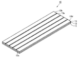
図1は、本発明の実施の形態1における超電導テープ線材を示す概略斜視図である。図1を参照して、本発明の実施の形態1における超電導テープ線材を説明する。本発明の実施の形態1における超電導テープ線材10は、図1に示すように、テープ状基板11と、中間薄膜層12と、超電導層13とを備えている。
(Embodiment 1)
FIG. 1 is a schematic perspective view showing a superconducting tape wire according to Embodiment 1 of the present invention. With reference to FIG. 1, the superconducting tape wire in Embodiment 1 of this invention is demonstrated. The
中間薄膜層12は、テープ状基板11上に形成されている。超電導層13は、中間薄膜層12上に形成され、一方端部13cから他方端部13dまで伸び、一方端部13cから他方端部13dまで延在する少なくとも1つの分割領域13aを含む。分割領域13aは、超電導層13bの臨界温度では超電導状態とならない領域である。
The intermediate
詳細には、分割領域13aは、超電導層13の長手方向(図1において一方端部13cから他方端部13dに延びる方向)に1つまたは複数並列に形成されている。実施の形態1では、一方端部13cと他方端部13dとは互いに対向している。
Specifically, one or more
なお、「端部」とは、端である場合、および、端までは達しておらず端近傍である場合の両方を意味する。実施の形態1では、図1に示すように、一方端部13cおよび他方端部13dは、端としている。
Note that the “end portion” means both the case where it is an end and the case where it is close to the end without reaching the end. In the first embodiment, as shown in FIG. 1, one
分割領域13aは、後述する製造方法からも分かるように、超電導層13にレーザ光を照射するといった手法によりその結晶性が乱された状態(超電導層13bより超電導状態となる臨界温度が低い、あるいは超電導状態にならないような結晶構造の状態)になっている部分、若しくは分割領域13aに相当する超電導層そのものの存在が無い状態になっている部分や、テープ状基板11までの深さ方向において材料がつながらない状態(分割領域13a下の中間薄膜層の一部または全部の存在が無い状態、またはテープ状基板11の裏面まで達して切断される場合を除き分割領域13a下の中間薄膜層およびテープ状基板の一部の存在が無い状態を含む)になっている部分である。すなわち、分割領域13aは、超電導層13が存在している場合であって超電導層の結晶性が乱された状態になっている部分、分割領域13aに相当する超電導層が存在しない状態になっている部分、分割領域13aに相当する超電導層とその下の中間薄膜層12の一部とが存在していない(中間薄膜層12の残部と基板11とは存在している)状態になっている部分、分割領域13aに相当する超電導層とその下の中間薄膜層12の全部とが存在していない(基板11は存在している)状態になっている部分、または分割領域13aに相当する超電導層とその下の中間薄膜層12の全部とその下の基板11の一部とが存在していない(基板11の残部は存在している)状態になっている部分である。
As can be seen from the manufacturing method described later, the divided
実施の形態1では、分割領域13aが4列形成されており、分割領域13a以外の部分の超電導層13bが5列形成されている。そのため、分割領域13aが形成されていない(長手方向と直交する方向における超電導層13bの幅と同じ幅を有する)超電導テープ線材が5列並列されている場合と同様のものとなる。そのため、超電導テープ線材10では、分割領域13aが形成できる程度の幅広としている。なお、分割領域13aは、特にこの構成に限定されない。たとえば、分割領域13aは、超電導層13の短手方向(図1において長手方向と直交する方向、すなわち一方端部13cおよび他方端部13dと平行な方向)に複数並列に形成されていてもよい。
In the first embodiment, four rows of divided
また、テープ状基板11は、Ni(ニッケル)またはNi合金系の配向テープを用いている。中間薄膜層12は、CeO2(セリア)およびYsZ(イットリア安定化ジルコニア)の少なくとも一方を含んでいるものを用いている。超電導層13は、HoBCO(ホルミウム系高温超電導材料:HoBa2Cu3Ox)を用いている。
The tape-
なお、テープ状基板11の材料は上述したNiまたはNi合金系に限られず他の材料(たとえば他の金属材料、あるいはその他のフレキシブルな材料)を用いてもよい。中間薄膜層12は、その上に超電導層13を形成できれば上述した材料に限られない。また、中間薄膜層12は1層に限らず、2層以上の複数層としてもよい。超電導層12としては上述したHoBCO以外のレア・アース系超電導材料、若しくは従来の金属系超電導材料や他の酸化物系超電導材料を用いてもよい。
The material of the tape-shaped
また、超電導層13の表面保護のために、超電導層13上にAg(銀)安定化層やCu(銅)安定化層などの表面保護層や安定化層(図示せず)を設けている。分割領域13a上の表面保護層は、分割領域13a以外の部分の超電導層13b上の表面保護層と同様の状態としてもよいし、分割領域13aと同様の状態としてもよい。
Further, in order to protect the surface of the
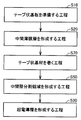
次に、図2および図3を参照して、超電導テープ線材10の製造方法について説明する。図2は、実施の形態1における超電導テープ線材10の製造方法を示すフローチャートである。図3は、実施の形態1での加工工程を示す概略模式図である。
Next, with reference to FIG. 2 and FIG. 3, the manufacturing method of the
まず、テープ状基板11を準備する工程(S10)を実施する。この工程(S10)では、上述したテープ状基板11を準備する。
First, a step (S10) of preparing the tape-shaped
次に、中間薄膜層12を形成する工程(S20)を実施する。この工程(S20)では、中間薄膜層12は、物理蒸着法や有機金属堆積法などによりテープ状基板11上に上述した材料を用いて形成される。
Next, a step (S20) of forming the intermediate
次に、超電導層13を形成する工程(S30)を実施する。この工程(S30)では、超電導層13は、中間薄膜層12上にPLD(Pulsed Laser Deposition)法またはスパッタ法などの物理蒸着法および有機金属堆積法(MOD法)の少なくともいずれか一方を含む方法で形成される。
Next, a step (S30) of forming the
次に、超電導層13は一方端部13cから他方端部13dまで伸び、超電導層13に一方端部13cから他方端部13dまで延在する少なくとも1つの分割領域13aを形成する加工工程(S40)を実施する。この工程(S40)では、分割領域13aは、超電導層13bの臨界温度では超電導状態とならない領域となるように行なう。
Next, the
実施の形態1では、工程(S40)は、レーザにより行なっている。具体的には、図3に示すように、レーザ(図3において矢印)は、超電導層13の長手方向に複数(図3において4列)並列に照射している。レーザを照射した部分は、分割領域13aとなる。つまり、レーザが照射された部分では、超電導層13が局所的に溶融・凝固することによって、当該部分の結晶性が乱れた状態(他の部分と対比するとその結晶構造に乱れが発生した状態)となる。このような結晶性が乱れた部分は、他の部分(超電導層13b)より超電導状態に遷移する臨界温度が低い、あるいは超電導状態にならないというようにその超電導特性が他の部分より劣化している。あるいはレーザ照射によって、超電導層の超電導材料そのものが飛散されて材料が無くなっている。そのため、このようにレーザが照射された部分が分割領域13aとなる。
In the first embodiment, the step (S40) is performed by a laser. Specifically, as shown in FIG. 3, a plurality of lasers (arrows in FIG. 3) are irradiated in parallel in the longitudinal direction of the superconducting layer 13 (four rows in FIG. 3). The portion irradiated with the laser becomes a divided
なお、工程(S40)は、分割領域13aを形成できれば、レーザにより行なわれることに特に限定されない。たとえば、分割領域13aは、当該部分に機械的な応力を加える(たとえば分割領域13aの平面形状に対応するブレード状の治具を押圧する)ことにより、超電導層13において結晶性を変更することにより形成してもよい。または、(テープ状基板11は切断せずに残存させる一方)超電導層12における分割領域13aを形成すべき部分を切断、除去、あるいは切削加工することにより、工程(S20)を実施することもできる。
Note that the step (S40) is not particularly limited to being performed by a laser as long as the divided
最後に、超電導層13上に表面保護層を形成する工程を実施する。この工程では、分割領域13aを形成した後に表面保護層を形成する。この場合は、分割領域13a上の表面保護層は、分割領域13a以外の部分の超電導層13b上の表面保護層と同様の状態となる。
Finally, a step of forming a surface protective layer on the
なお、表面保護層を形成する工程は、超電導層13を形成する工程(S30)の後に実施してもよい。この場合は、表面保護層が形成されたのちに、加工工程(S40)を実施する。この場合は、分割領域13a上の表面保護層は、分割領域13aと同様の状態となる。
The step of forming the surface protective layer may be performed after the step of forming the superconducting layer 13 (S30). In this case, the processing step (S40) is performed after the surface protective layer is formed. In this case, the surface protective layer on the divided
上記工程(S10〜S40)を行なうことにより、実施の形態1における超電導テープ線材10を製造することができる。
次に、実施の形態1における超電導テープ線材10の動作について説明する。超電導テープ線材10において一方端部13cと他方端部13dとの間に電圧を印加して電流を流すと、一定の条件(たとえば超電導層13bが超電導状態になる温度にまで超電導テープ線材10を冷却した状態)では、分割領域13a以外の部分の超電導層13bに超電導状態で電流を流すことができる。このとき、複数の超電導層13bは互いに電気的に独立した導電線とみなすことができるので、複数の超電導線が並列に配置された状態と等価な状態となる。
Next, the operation of the
また、超電導テープ線材10の動作については、上述した動作に限られない。たとえば、分割領域13a以外の部分の5の超電導層13bを直列に接続することもできる。具体的にはそれぞれの超電導層13bの端部で近接の他の超電導層13bと電気的に接続する。そして、電流を流すと、1本の導電線とみなすことができるので、1本の長尺な線材と等価な状態となる。
Further, the operation of the
以上説明したように、本発明の実施の形態1における超電導テープ線材10の製造方法によれば、テープ状基板11を準備する工程(S10)と、テープ状基板11上に中間薄膜層12を形成する工程(S20)と、中間薄膜層12上に超電導層13を形成する工程(S30)と、超電導層13は一方端部13cから他方端部13dまで伸び、超電導層13に一方端部13cから他方端部13dまで延在する少なくとも1つの分割領域13aを形成する加工工程(S40)とを備えている。分割領域13aは、超電導層13bの臨界温度では超電導状態とならない領域であることを特徴とする。そのため、分割領域13aを形成することにより、1の超電導テープ線材10で、分割領域13a以外の部分の超電導層13bを構成する領域数の超電導テープ線材を集めたものと同様の効果を有する超電導テープ線材10を容易に製造することができる。また、幅広の超電導テープ線材10を用いれば、たとえ長尺でなくてもその長さの領域数の超電導テープ線材を集めたのと同様の効果を有する超電導テープ線材10を製造することができる(そのトータル長さが、(幅広の超電導テープ線材10の長手方向の長さ)×(超電導層13bの領域数)となる、複数の超電導テープ線材が並列に配置された構造体を製造できる)。よって、長尺な線材を用いずに、幅広の超電導テープ線材10を分割して、並列な複数の幅の狭い超電導テープ線材からなる構造体を形成できる。このような構造体では分割数を増やすことによって超電導テープ線材のトータル長さを長くすることができるので、長尺な超電導テープ線材と同様に用いることができる超電導テープ線材10を工業化することは可能となる。
As described above, according to the method of manufacturing
上記超電導テープ線材10の製造方法において好ましくは、加工工程(S40)は、レーザにより行なわれる。これにより、分割領域13aを容易に形成することができる。また、レーザの照射領域の幅、位置、または深さを変更することで、分割領域13aの幅、位置、または深さを容易に変更できる。このため、並列に配置された超電導テープ線材とみなせる超電導層13bの幅や分割数を容易に変更できる。
Preferably, in the method for manufacturing
上記超電導テープ線材10の製造方法において好ましくは、加工工程(S40)は、超電導層13の長手方向に1つまたは複数並列に分割領域13aを形成するように行なわれる。これにより、分割領域13a以外の部分の複数の超電導層13bにおいて、複数本の電流パスを確保できる。または、超電導層13bを直列に接続して電流を流すことによって、1本の長尺な線材と等価な線材を実現することができる。よって、安価で高性能な超電導テープ線材10を製造できるので、工業化が可能となる。
Preferably, in the method for manufacturing the
上記超電導テープ線材10の製造方法において好ましくは、中間薄膜層12は物理蒸着法により形成されている。物理蒸着法としては、PLD法やスパッタ法などの特性に優れた膜を形成できる手法を用いることができるので、優れた膜質の中間薄膜層12を容易に形成することができる。
In the method for manufacturing the
上記超電導テープ線材10の製造方法において好ましくは、超電導層13は、物理蒸着法および有機金属堆積法の少なくともいずれか一方を含む方法により形成される。物理蒸着法(たとえばPLD法など)は超電導層の特性に優れ、MOD法は、低コストという点で優れている。そのため、超電導テープ線材10の工業化が可能となる。
In the method for manufacturing the
また、本発明の実施の形態1における超電導テープ線材10は、テープ状基板11と、テープ状基板11上に形成された中間薄膜層12と、中間薄膜層12上に形成され、一方端部13cから他方端部13dまで伸び、一方端部13cから他方端部13dまで延在する少なくとも1つの分割領域13aを含む超電導層13とを備え、分割領域13aは、超電導層13bの臨界温度では超電導状態とならない領域であることを特徴としている。そのため、分割領域13aを形成することにより、1の超電導テープ線材10は、分割領域13a以外の部分の超電導層13bを構成する領域数の超電導テープ線材を集めたものと同様の効果を有する。
The
また、幅広の超電導テープ線材10を用いれば、たとえ長尺でなくてもその長さの領域数の超電導テープ線材を集めたものと同様の効果を有する。そのため、超電導テープ線材10は、長尺である必要がない。よって、超電導テープ線材10の工業化は容易となる。
Moreover, if the wide
上記超電導テープ線材10において好ましくは、テープ状基板11は、NiまたはNi合金系の配向金属テープであり、中間薄膜層はCeO2およびYsZの少なくとも一方を含んでおり、超電導層12は、HoBCOを含んでいる。これにより、テープ状基板11の配向性を生かす構造とすることができる。そのため、超電導テープ線材10は、実用上必要とされる大きな臨界電流値(Ic)および臨界電流密度(Jc)を得ることができる。さらに、テープ状基板11として用いる材料の選択の自由度を大きくできる。よって、超電導テープ線材10の工業化が可能となる。
Preferably in the
次に、図4を参照して、実施の形態1の超電導テープ線材10の変形例について説明する。図4は、実施の形態1の変形例における超電導テープ線材を示す概略斜視図である。変形例における超電導テープ線材20の構成は、基本的には本発明の実施の形態1における超電導テープ線材10と同様の構成を備えるが、分割領域13aの形状において、図1に示した超電導テープ線材10と異なる。
Next, with reference to FIG. 4, the modification of the
詳細には、分割領域13aは、端までは達しておらず端近傍である一方端部13cから他方端部13dまで延在している。変形例では、端近傍である分割領域13aの先端とその近傍である端との幅Wは、5cm〜20cmとしている。なお、幅Wは超電導テープ線材20の長さや分割領域13aの形成される長さによらず、5cm〜20cmとすることが好ましい。
Specifically, the divided
なお、変形例の超電導テープ線材20における分割領域13aは、実施の形態1の超電導テープ線材10における分割領域13aの場合に加えて、分割領域13aに相当する超電導層、その下の中間薄膜層12および基板11が、レーザ加工や機械加工などで切れ目を入れる手法により存在していない状態を含む。すなわち、端までは達していない場合の分割領域13aは、超電導層13が存在している場合であって超電導層の結晶性が乱された状態になっている部分、分割領域13aに相当する超電導層が存在しない状態になっている部分、分割領域13aに相当する超電導層とその下の中間薄膜層12の一部とが存在していない(中間薄膜層12の残部と基板11とは存在している)状態になっている部分、分割領域13aに相当する超電導層とその下の中間薄膜層12の全部とが存在していない(基板11は存在している)状態になっている部分、分割領域13aに相当する超電導層とその下の中間薄膜層12の全部とその下の基板11の一部とが存在していない(基板11の残部は存在している)状態になっている部分、または分割領域13aに相当する超電導とその下の中間薄膜層12とその下の基板11とが存在していない(切れ目が入った)状態になっている部分である。
In addition, the divided
また、超電導テープ線材20の製造方法の構成は、基本的には本発明の実施の形態1における超電導テープ線材10の製造方法と同様の構成を備えるが、加工工程(S40)において、図2に示した超電導テープ線材10の製造方法と異なる。
Moreover, the structure of the manufacturing method of the
詳細には、実施の形態1における超電導テープ線材10の製造方法における加工工程(S40)で、分割領域13aを、図4に示すように、端近傍(端から幅W)まで延在するように形成する。上記工程を行なうことにより、実施の形態1の変形例における超電導テープ線材20を製造することができる。
Specifically, in the processing step (S40) in the method of manufacturing the
超電導テープ線材20を動作させるときには、幅Wに相当するテープ状基板11、中間薄膜層12、および超電導層13を切断する。これにより、実施の形態1の超電導テープ線材10と同様の動作となる。なお、幅Wに相当するテープ状基板11、中間薄膜層12、および超電導層13を切断することに特に限定されない。たとえば、一方端部または両端部を切断せずに、分割領域13aで2の領域に区分された領域の先端を接続することにより、1本の長尺な超電導テープ線材を製造することもできる。
When the
以上説明したように、実施の形態1の変形例における超電導テープ線材20によれば、幅Wを残して分割領域13aを形成する。そのため、実用性を向上することができる。
As described above, according to the
(実施の形態2)
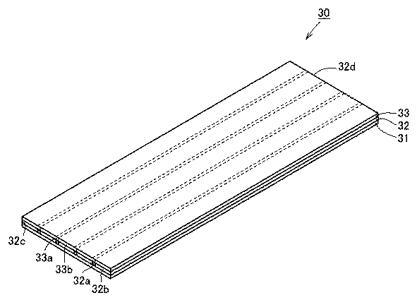
図5は、実施の形態2における超電導テープ線材を示す概略斜視図である。図5を参照して、本発明の実施の形態2における超電導テープ線材を説明する。本発明の実施の形態2における超電導テープ線材30は、図5に示すように、テープ状基板31と、中間薄膜層32と、超電導層33とを備えている。
(Embodiment 2)
FIG. 5 is a schematic perspective view showing the superconducting tape wire according to the second embodiment. With reference to FIG. 5, the superconducting tape wire in Embodiment 2 of this invention is demonstrated. The
中間薄膜層32は、テープ状基板31上に形成され、一方端部32cから他方端部32dまで伸び、一方端部32cから他方端部32dまで延在する少なくとも1つの中間層分割領域32aを含む。中間薄膜層32は、1層または2層以上としている。超電導層33は、中間薄膜層32上に形成される。
The intermediate
中間層分割領域32a上の超電導層領域33aは、超電導層33bの臨界温度では超電導状態とならない領域としている。すなわち、中間層分割領域32aは、中間層分割領域32a以外の部分の中間薄膜層32b上の超電導層33bが超電導状態となるとき、中間層分割領域32a上の超電導層領域33aが超電導状態とならないような構造としている。
The
詳細には、中間層分割領域32aは、超電導層33の長手方向に複数並列に形成されている。実施の形態2では、中間層分割領域32aが4列形成されており、中間層分割領域32a以外の部分の中間薄膜層32bが5列形成されている。
Specifically, a plurality of intermediate
中間層分割領域32a上の超電導層領域33aは、中間層分割領域32aの長手方向に複数並列に形成されている。実施の形態2では、中間層分割領域32a上の超電導層領域33aが4列形成されており、中間層分割領域32a以外の領域上の超電導層33bが5列形成されている。そのため、中間層分割領域32aが形成されていない同じ長さの超電導テープ線材が5列並列されている場合と同様のものとなる。
A plurality of
実施の形態2では、テープ状基板31、中間薄膜層32、超電導層33は、実施の形態1におけるテープ状基板11、中間薄膜層12、超電導層13と同様の材料を用いているが、特にこの構成に限定されない点についても実施の形態1と同様である。なお、図示していないが、超電導テープ線材30は表面保護層を含む点においても実施の形態1と同様である。
In the second embodiment, the tape-
次に、図6を参照して、超電導テープ線材30の製造方法について説明する。図6は、実施の形態2における超電導テープ線材30の製造方法を示すフローチャートである。
Next, with reference to FIG. 6, the manufacturing method of the
まず、テープ状基板31を準備する工程(S10)を実施する。次に、テープ状基板31上に中間薄膜層32を形成する工程(S20)を実施する。この工程(S10,S20)は、実施の形態1の製造方法における工程(S10,S20)と同様であるので、その説明は繰り返さない。
First, a step (S10) of preparing the tape-shaped
次に、中間薄膜層32は一方端部32cから他方端部32dまで伸び、中間薄膜層32に一方端部32cから他方端部32dまで延在する少なくとも1つの中間層分割領域32aを形成する加工工程(S50)を実施する。この工程(S50)では、中間層分割領域32a上の超電導層領域33aは、超電導層33bの臨界温度では超電導状態とならない領域となるように実施する。
Next, the intermediate
実施の形態2では、工程(S50)は、実施の形態1における工程(S40)と同様に、レーザにより行なっているが、レーザにより行なわれることに特に限定されず、実施の形態1における工程(S40)に関する説明で述べた機械的加工法など任意の方法を用いることができる。 In the second embodiment, the step (S50) is performed by a laser similarly to the step (S40) in the first embodiment. However, the step (S50) is not particularly limited to being performed by the laser, and the step (step S50) in the first embodiment ( Any method such as the mechanical processing method described in the description of S40) can be used.
また、中間薄膜層32が2層以上の複数層からなる場合、少なくとも最上層(テープ状基板31から最も離れた位置に形成された層)に中間層分割領域32aが形成されていればよい。中間層分割領域32aは、中間薄膜層32b上に形成される超電導層33bより結晶性の劣る(超電導特性の劣る、あるいは超電導特性を発揮しない結晶構造である)超電導層領域33aをその上に形成できれば、どのような構造であってもよい。たとえば、中間層分割領域32aはその上部表面(超電導層33側の表面)の膜質が、中間薄膜層32bの上部表面の膜質と異なっていてもよい。また、中間薄膜層32が複数の層からなる場合、超電導層33に接触する最上層または当該最上層の超電導層33側の表面に中間層分割領域32aが形成されていてもよいし、中間層分割領域32aは上述した複数の層を貫通するように形成されていてもよい。
Moreover, when the intermediate
次に、中間薄膜層32上に超電導層33を形成する工程(S30)を実施する。この工程(S30)を行なうと、中間層分割領域32a上の超電導層領域33aの結晶性は、中間層分割領域32a以外の部分の中間薄膜層32b上の超電導層33bの結晶性と異なる。
Next, the process (S30) of forming the
次に、表面保護層を形成する工程を実施する。上記工程(S10,S20,S50,S30)を行なうことにより、実施の形態2における超電導テープ線材30を製造することができる。
Next, a step of forming a surface protective layer is performed.
超電導テープ線材30の動作は、実施の形態1における超電導テープ線材10の動作と同様であるので、その説明は繰り返さない。
Since the operation of
以上説明したように、本発明の実施の形態2における超電導テープ線材30の製造方法によれば、テープ状基板31を準備する工程(S10)と、テープ状基板31上に中間薄膜層32を形成する工程(S20)と、中間薄膜層32は一方端部から他方端部まで伸び、中間薄膜層32に一方端部から他方端部まで延在する少なくとも1つの中間層分割領域32aを形成する加工工程(S50)と、中間薄膜層32上に超電導層33を形成する工程(S30)とを備え、中間層分割領域32a上の超電導層領域33aは、超電導層33bの臨界温度では超電導状態とならない領域であることを特徴としている。中間層分割領域32aを形成することにより、1の超電導テープ線材30で、中間層分割領域32a以外の中間薄膜層32b上の超電導層33bの領域数の超電導テープ線材を集めた(直列に配置した)ものと同様の効果を有する超電導テープ線材30を容易に製造することができる。よって、長尺な線材を用いずに、幅広の超電導テープ線材30を用いることができるので、超電導テープ線材30を工業化することは可能となる。
As described above, according to the method of manufacturing
本発明の実施の形態2における超電導テープ線材30によれば、テープ状基板31と、テープ状基板31上に形成され、一方端部から他方端部まで伸び、一方端部から他方端部まで延在する少なくとも1つの中間層分割領域32aを含む中間薄膜層32と、中間薄膜層32上に形成された超電導層33とを備え、中間層分割領域32a上の超電導層33aは、超電導層33bの臨界温度では超電導状態とならない領域であることを特徴としている。中間層分割領域32aを形成することにより、1の超電導テープ線材30は、中間層分割領域32aにより区分された中間薄膜層32b上の超電導層33bを構成する領域数の超電導テープ線材を集めたものの効果と同様の効果を有する。
According to the
(実施の形態3)
図7は、本発明の実施の形態3における超電導機器を示す概略斜視図である。図7を参照して、本発明の実施の形態3における超電導機器を説明する。本発明の実施の形態3における超電導機器は超電導コイルとしている。実施の形態3における超電導コイル40は、実施の形態1における超電導テープ線材10を用いて製造されている。
(Embodiment 3)
FIG. 7 is a schematic perspective view showing a superconducting device according to Embodiment 3 of the present invention. With reference to FIG. 7, a superconducting device according to Embodiment 3 of the present invention will be described. The superconducting device in Embodiment 3 of the present invention is a superconducting coil.
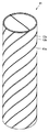
超電導コイル40は、図7に示すように、分割領域13aが形成された超電導層13とテープ状基板11とを含む超電導テープ線材10(図1参照)が巻かれることにより巻き形状体41,42,43が構成され、分割領域13aは、分割領域13a以外の部分の超電導層13bが超電導状態となるとき、超電導状態とならないような構造としている。
As shown in FIG. 7, the
なお、上記「巻き形状体」とは、筒状または中空でない棒体であり、その断面形状は丸、多角形、一部凹の形状など任意の形状であることを意味する。 In addition, the above-mentioned “roll-shaped body” is a cylindrical body or a non-hollow rod body, and means that the cross-sectional shape is an arbitrary shape such as a circle, a polygon, or a partially concave shape.
実施の形態3では、超電導コイル40は、3枚の超電導テープ線材10からそれぞれが構成される巻き形状体41〜43を備えている。超電導テープ線材10は、らせん状に巻かれることにより円筒となる巻き形状体41〜43を構成する。そして、超電導コイル40の内側から順に巻き形状体41,42,43が配置されており、最外層には超電導テープ線材10からなる巻き形状体43が配置されている3層コイルとしている。なお、超電導コイル40を構成する巻き形状体41〜43は、超電導コイル40の内周側に位置するものほどその外径が小さくなっている。
In the third embodiment, the
巻き形状体41,42,43を構成する超電導テープ線材10は、それぞれ、分割領域13aにより区分された2以上の領域がらせん状になるように、分割領域13aが形成された超電導層12とテープ状基板11とを含む超電導テープ線材10が円筒状に巻かれている。これにより、巻き形状体41〜43を形成している。
The superconducting
実施の形態3では、図7に示すように、最外層である超電導テープ線材10からなる巻き形状体43において、4列の分割領域13aが形成されて区分された5列の領域の超電導層13bのうち、任意の領域13Bに着目する。巻き形状体43の任意の領域13Bは、巻き形状体42の領域13Bに相当する領域と、たとえばはんだで接続されている。同様に、巻き形状体42の領域13Bに相当する領域は、巻き形状体41の領域13Bに相当する領域と、たとえばはんだで接続されている。このようにして、巻き形状体41〜43におけるそれぞれの領域が接続されている。
In the third embodiment, as shown in FIG. 7, in the
なお、上記の構成に特に限定されず、たとえばコイルは1層であってもよい(1つの巻き形状体から構成されていてもよい)。また、分割領域13aは2以上であれば、形成可能な数の領域に分割してもよい。また、コイルを構成する巻き形状体41〜43のそれぞれは、1枚ではなく2枚以上(たとえば3枚)の超電導テープ線材10を組合せて形成してもよい。たとえば、3枚の超電導テープ線材10のそれぞれの一方端部13cについて所定の加工(らせん状に巻くため端部を斜めに切断するなどの加工)を行なったあと、当該加工後の端面の端を互いに接続して、巻き形状体の端部の円形開口部を構成する。そして、3つの超電導テープ線材をらせん状に巻きながら接続して1つのコイルを形成する(つまり、1つのコイルの外周側面を複数(たとえば3つ)の超電導テープ線材10により構成する)。このようにすれば、複数の超電導テープ線材10を用いて大口径のコイルを形成することができる。
In addition, it is not specifically limited to said structure, For example, a coil may be one layer (it may be comprised from one winding shape body). Moreover, as long as the
なお、図示していないが、超電導コイル40は、表面保護層を超電導層13上に備えている。
Although not shown, the
次に、図8〜図10を参照して、超電導コイル40の製造方法について説明する。図8は、実施の形態3における超電導コイル40の製造方法を示すフローチャートである。図9は、1枚の超電導テープ線材10を用いて製造された1層のコイルの模式図である。図10は、3枚の超電導テープ線材からそれぞれ形成された巻き形状体41〜43を用いて3層のコイルを製造する模式図である。
Next, a method for manufacturing the
まず、超電導テープ線材10の製造方法により最内層である巻き形状体41である超電導コイルを製造する工程を実施する。実施の形態3では、超電導コイルは、実施の形態1における超電導テープ線材10を用いている。そのため、具体的には、図8に示すように、まず、テープ状基板11を準備する工程(S10)を実施する。次に、テープ状基板11上に中間薄膜層を形成する工程(S20)を実施する。次に、超電導層13を形成する工程(S30)を実施する。次に、超電導層13は一方端部13cから他方端部13dまで伸び、超電導層13に一方端部13cから他方端部13dまで延在する少なくとも1つの分割領域13aを形成する加工工程(S40)を実施する。これらの工程(S10〜S40)は、実施の形態1における工程(S10〜S40)と同様であるため、その説明は繰り返さない。
First, the process of manufacturing the superconducting coil which is the winding
次に、超電導テープ線材10を巻く工程(S60)を実施する。この工程(S60)では、巻き形状体41を形成する。
Next, the process (S60) of winding the
実施の形態3では、図9に示すように、分割領域13aにより区分された2以上の領域がらせん状になるように、分割領域13aが形成された超電導テープ線材10を円筒状に巻く。この際に、超電導テープ線材10の長手方向の辺である境界線41aが重ならず、かつ隙間ができないようにらせん状に巻いている。
In the third embodiment, as shown in FIG. 9, the
そして、図10に示すように、3つの超電導テープ線材10について工程(S60)を実施することにより、それぞれ巻き形状体41,42,43を形成する。次いで、図10に示すように、巻き形状体41,42,43を順に重ねる(同心円状に配置する、あるいは巻き形状体41の外周を覆うように巻き形状体42を配置し、さらに巻き形状体42の外周を覆うように巻き形状体43を配置する)。なお、巻き形状体41,42,43を重ねることができるように、その円筒の内径をその順に大きくしている。
Then, as shown in FIG. 10, by performing the step (S60) on the three
上記工程(S10〜S60)を行なうことにより、実施の形態3における超電導コイル40を製造することができる。そして、上述したように各巻き形状体41〜43の対応する領域(超電導層13b)が互いに電気的に接続される。
次に、図7を参照して、超電導コイル40の動作について説明する。超電導コイル40に電流を流すために、電源を接続する。超電導コイル40は、各巻き形状体41,42,43において分割領域12aが形成されて区分された領域ごとに接続されている。領域ごとに接続された巻き形状体41、42,43において、接続された先端と電源とを接続する。
Next, the operation of the
実施の形態3では、巻き形状体43における4列の分割領域13aが形成されて区分された5の領域の超電導層13bのうち任意の領域13Bの端部(図7においてたとえば下側)と、巻き形状体42における領域13Bの端部(図7においてたとえば下側)とを接続している。同様に、巻き形状体42における領域13Bの他方の端部(図7においてたとえば上側)と、巻き形状体41における領域13Bの端部(図7においてたとえば上側)とを接続している。これにより、巻き形状体41〜43は、電気的に接続される。
In the third embodiment, the end of any region 13B (for example, the lower side in FIG. 7) of the
そして、接続されてなる超電導コイル40において、電源をONにすると、巻き形状体41の領域13B(図7においてたとえば上方向)、巻き形状体42の領域13B(図7においてたとえば下方向)、巻き形状体43の領域13B(図7においてたとえば上方向)を電流が流れる。このようにして、5列の領域それぞれに電流を流し、一定の条件下で超電導状態とすることができる。
When the power is turned on in the connected
なお、上記構成に特に限定されず、たとえば巻き形状体41,42,43のそれぞれの超電導テープ線材10において分割領域13a以外の部分の5の超電導層13bの端部で近接の他の超電導層13bを直列に接続する。そして、巻き形状体41,42,43を接続すると、1本の導電線とみなすことができる。すなわち、1本の長尺な線材と等価な状態となる。そして、電源をその先端に接続すると、必要な電源は1つとなる。これにより、電源の数を減らすことができるので、安価な超電導コイルを製造することができる。この超電導コイルに電流を流すと、一定の条件下、1の流路において超電導状態とすることができる。
In addition, it is not specifically limited to the said structure, For example, in the
以上説明したように、本発明の実施の形態3における超電導機器の一例である超電導コイル40によれば、実施の形態1における超電導テープ線材10を用いた超電導機器としている。そのため、分割領域13aを形成することにより、1の超電導テープ線材10は、分割領域13a以外の部分の超電導層13bを構成する領域数の超電導テープ線材を集めたものと同様の効果を有する超電導テープ線材となり、当該超電導テープ線材を用いて超電導コイル40を容易に製造できる。
As described above, according to the
また、本発明の実施の形態3における超電導機器の一例である超電導コイル40の製造方法によれば、実施の形態1における超電導テープ線材10の製造方法により超電導テープ線材10を製造する工程(S10〜S40)と、超電導テープ線材10を巻く工程(S60)とを備えている。そのため、分割領域13aを形成することにより、1の超電導テープ線材10で、分割領域13a以外の部分の超電導層13bを構成する領域数の超電導テープ線材を集めたものと同様の効果を有する超電導テープ線材10を用いて超電導コイル40を容易に製造することができる。よって、長尺な線材を用いずに、幅広の超電導テープ線材10を用いることができるので、超電導コイル40を工業化することは可能となる。
In addition, according to the method for manufacturing
次に、実施の形態3の超電導コイル40の変形例について説明する。変形例における超電導機器の一例である超電導コイルの構成は、基本的には本発明の実施の形態3における超電導コイル40と同様の構成を備えるが、中間薄膜層において中間層分割領域が形成されている点において、図7に示した超電導コイル40と異なる。
Next, a modification of the
詳細には、実施の形態2における超電導テープ線材30を用いている。具体的には、図5に示すように、超電導テープ線材30は、テープ状基板31と、中間薄膜層32と、超電導層33とを備えている。超電導テープ線材30を中間層分割領域32a上の超電導層33aにより区分された2以上の領域がらせん状になるように、中間層分割領域32aが形成された超電導テープ線材30を円筒状に巻かれた巻き形状体として、変形例における超電導コイルを形成している。
Specifically, the
次に、図11を参照して、実施の形態3の変形例における超電導コイルの製造方法について説明する。図11は、変形例における超電導コイルの製造方法を示すフローチャートである。 Next, with reference to FIG. 11, a method for manufacturing a superconducting coil in a modification of the third embodiment will be described. FIG. 11 is a flowchart showing a method of manufacturing a superconducting coil in a modified example.
実施の形態3の変形例における超電導コイルの製造方法の構成は、基本的には本発明の実施の形態3における超電導コイル40の製造方法と同様の構成を備えるが、実施の形態2における超電導テープ線材を用いて製造している点において、図8に示した超電導コイル40の製造方法と異なる。
The configuration of the superconducting coil manufacturing method in the modification of the third embodiment is basically the same as the manufacturing method of the
まず、実施の形態2における超電導テープ線材30の製造方法により超電導テープ線材30を製造する工程を実施する。具体的には、図11に示すように、テープ状基板31を準備する工程(S10)を実施する。次に、テープ状基板31上に中間薄膜層32を形成する工程(S20)を実施する。次に、中間薄膜層32は一方端部から他方端部まで伸び、中間薄膜層32に一方端部から他方端部まで延在する少なくとも1つの中間層分割領域32aを形成する加工工程(S50)を実施する。次に、中間薄膜層32上に超電導層33を形成する工程(S30)を実施する。これらの工程(S10,S20,S50,S30)は、実施の形態2の製造方法における工程(S10,S20,S50,S30)と同様であるので、その説明は繰り返さない。
First, the process of manufacturing the
次に、超電導テープ線材30を巻く工程(S60)を実施する。この工程(S60)は、実施の形態3の製造方法における工程(S60)と同様であるので、その説明は繰り返さない。
Next, the process (S60) of winding the
上記工程(S10,S20,S50,S30,S60)を行なうことにより、各巻き形状体41〜43を形成し、これらの巻き形状体41〜43を組合せることによって実施の形態3の変形例における超電導コイルを製造することができる。
By performing the above steps (S10, S20, S50, S30, S60), the respective wound-shaped
以上説明したように、実施の形態3の変形例における超電導機器の一例である超電導コイルによれば、実施の形態2における超電導テープ線材30を用いている。これにより、中間層分割領域32aを有する中間薄膜層32を備える超電導コイルとなる。
As described above, according to the superconducting coil which is an example of the superconducting device in the modification of the third embodiment, the
以上説明したように、実施の形態3の変形例における超電導機器の一例である超電導コイルの製造方法によれば、実施の形態2における超電導テープ線材30の製造方法により超電導テープ線材30を製造する工程(S10,S20,S50,S30)と、製造する工程(S10,S20,S50,S30)により製造された超電導テープ線材30を巻く工程(S60)とを備えている。そのため、中間層分割領域32aを有する中間薄膜層32を備える超電導コイルを容易に製造することができる。
As described above, according to the method of manufacturing a superconducting coil which is an example of the superconducting device in the modification of the third embodiment, the process of manufacturing the
(実施の形態4)
本発明の実施の形態4は、超電導機器の一例である超電導コイルである。本発明の実施の形態4における超電導コイルは、基本的には図7に示す実施の形態3における超電導コイル40と同様の構成であるが、製造方法が異なる。そのため、実施の形態4における超電導コイルについてその説明は繰り返さない。
(Embodiment 4)
Embodiment 4 of the present invention is a superconducting coil which is an example of a superconducting device. The superconducting coil in the fourth embodiment of the present invention has basically the same configuration as that of the
次に、図12および図13を参照して、本発明の実施の形態4における超電導コイルの製造方法について説明する。図12は、本発明の実施の形態4における超電導コイルの製造方法を示すフローチャートである。図13は、実施の形態4における加工工程を示す概略模式図である。 Next, with reference to FIG. 12 and FIG. 13, the manufacturing method of the superconducting coil in Embodiment 4 of this invention is demonstrated. FIG. 12 is a flowchart showing a method for manufacturing a superconducting coil according to Embodiment 4 of the present invention. FIG. 13 is a schematic diagram showing a processing step in the fourth embodiment.
まず、テープ状基板を準備する工程(S10)を実施する。次に、テープ状基板上に中間薄膜層を形成する工程(S20)を実施する。次に、中間薄膜層32上に超電導層33を形成する工程(S30)を実施する。これらの工程(S10〜S30)は、実施の形態1の製造方法における工程(S10〜S30)と同様であるので、その説明は繰り返さない。
First, a step (S10) of preparing a tape-shaped substrate is performed. Next, a step (S20) of forming an intermediate thin film layer on the tape-like substrate is performed. Next, the process (S30) of forming the
次に、超電導テープ線材を巻く工程(S60)を実施する。この工程(S60)は、実施の形態3の製造方法における工程(S60)と同様であるので、その説明は繰り返さない。 Next, the process (S60) of winding a superconducting tape wire is performed. Since this step (S60) is the same as step (S60) in the manufacturing method of the third embodiment, description thereof will not be repeated.
次に、巻いた超電導テープ線材の超電導層において、一方の端部に位置する一方端部から他方の端部に位置する他方端部まで伸び、超電導層を一方端部から他方端部まで延在する2以上の領域に区分する分割領域を形成する加工工程(S40)を実施する。この工程(S40)では、分割領域は、超電導層の臨界温度では超電導状態とならない領域となるように行なわれる。 Next, in the superconducting layer of the wound superconducting tape wire, it extends from one end located at one end to the other end located at the other end, and the superconducting layer extends from one end to the other end. A processing step (S40) for forming a divided region divided into two or more regions is performed. In this step (S40), the division region is performed so as to be a region that does not enter the superconducting state at the critical temperature of the superconducting layer.
実施の形態4における工程(S40)では、たとえば、工程(S60)により形成された巻き形状体の両端を固定する。固定するために、固定部材を設けてもよい。固定部材を設けることにより、超電導コイルの形状を維持しやすくなる。なお、この工程(S20)では、巻き形状体に分割領域を形成できれば、特にこれに限定されない。たとえば、超電導テープ線材を巻いた状態を維持できれば、分割領域を形成できる。 In step (S40) in the fourth embodiment, for example, both ends of the wound body formed in step (S60) are fixed. In order to fix, a fixing member may be provided. By providing the fixing member, the shape of the superconducting coil can be easily maintained. In addition, in this process (S20), if a division area can be formed in a winding shape body, it will not specifically limit to this. For example, if the state where the superconducting tape wire is wound can be maintained, the divided regions can be formed.
そして、図13に示すように、たとえば超電導テープ線材の超電導層53をレーザで照射して分割領域53aを形成している。具体的には、レーザは、巻き形状体の超電導層53をらせん状に照射して、分割領域53aを形成する。実施の形態4では、分割領域53aは4列並列に形成している。これにより、分割領域53aにより区分された5の領域の超電導層52bがらせん状になるように円筒状に巻かれる巻き形状体を製造することができる。
Then, as shown in FIG. 13, for example, a
上記工程(S10,S20,S30,S60,S40)を行なうことにより、巻き形状体を製造でき、当該巻き形状体を組合せることによって実施の形態4における超電導コイルを製造することができる。 By performing the above steps (S10, S20, S30, S60, S40), a wound-shaped body can be manufactured, and the superconducting coil in Embodiment 4 can be manufactured by combining the wound-shaped bodies.
実施の形態4における超電導コイルの動作は、実施の形態3における超電導コイル40と同様であるので、その説明は繰り返さない。
Since the operation of the superconducting coil in the fourth embodiment is similar to that of
以上説明したように、実施の形態4における超電導機器の一例である超電導コイルの製造方法によれば、テープ状基板を準備する工程(S10)と、テープ状基板上に中間薄膜層を形成する工程(S20)と、中間薄膜層32上に超電導層33を形成する工程(S30)と、超電導テープ線材を巻く工程(S60)と、巻いた超電導テープ線材の超電導層53において、一方の端部に位置する一方端部から他方の端部に位置する他方端部まで伸び、超電導層53を一方端部から他方端部まで延在する2以上の領域に区分する分割領域53aを形成する加工工程(S40)とを備え、加工工程(S40)は、超電導層53のうち分割領域53aとなるべき部分を、分割領域以外の部分の超電導層53bが超電導状態となるとき、超電導状態とならないような構造に加工する工程を含む。これにより、超電導テープ線材を巻き形状体とした後に、加工工程(S40)を実施することができる。そのため、分割領域53aを形成することにより、1の超電導テープ線材で、分割領域53a以外の部分の超電導層53bを構成する領域数の超電導テープ線材を集めたもののと同様の効果を有する超電導テープ線材を用いて超電導コイルを容易に製造することができる。よって、超電導コイルを工業化することは可能となる。
As described above, according to the method of manufacturing a superconducting coil which is an example of the superconducting device in the fourth embodiment, the step of preparing a tape-like substrate (S10) and the step of forming an intermediate thin film layer on the tape-like substrate (S20), the step (S30) of forming the
(実施の形態5)
本発明の実施の形態5は、超電導機器の一例である超電導コイルである。本発明の実施の形態5における超電導コイルは、基本的には図7に示す実施の形態3における超電導コイル40と同様の構成であるが、中間薄膜層を備えている点および製造方法が異なる。
(Embodiment 5)
Embodiment 5 of the present invention is a superconducting coil which is an example of a superconducting device. The superconducting coil according to the fifth embodiment of the present invention has basically the same configuration as that of the
実施の形態5における超電導コイルは、テープ状基板と、中間薄膜層と、超電導層とを備えている。中間薄膜層は、テープ状基板上に形成され、一方端部から他方端部まで伸び、一方端部から他方端部まで延在する少なくとも1つの中間層分割領域を含む。超電導層は、中間薄膜層上に形成されている。中間層分割領域が形成された中間薄膜層とテープ状基板と超電導層とを含む超電導テープ線材が巻かれることにより巻き形状体が構成されている。中間層分割領域上の超電導層領域は、超電導層の臨界温度では超電導状態とならない領域としている。 The superconducting coil in the fifth embodiment includes a tape-like substrate, an intermediate thin film layer, and a superconducting layer. The intermediate thin film layer is formed on the tape-like substrate and includes at least one intermediate layer division region extending from one end to the other end and extending from the one end to the other end. The superconducting layer is formed on the intermediate thin film layer. A wound body is formed by winding a superconducting tape wire including an intermediate thin film layer in which an intermediate layer division region is formed, a tape-like substrate, and a superconducting layer. The superconducting layer region on the intermediate layer dividing region is a region that does not enter the superconducting state at the critical temperature of the superconducting layer.
そして、テープ状基板と、中間層分割領域により区分された2以上の領域がらせん状になるように中間層分割領域が形成された中間薄膜層と、超電導層とを含む超電導テープ線材により円筒状に巻かれた巻き形状体が構成されている。 A cylindrical shape is formed by a superconducting tape wire including a tape-like substrate, an intermediate thin film layer in which an intermediate layer division region is formed so that two or more regions divided by the intermediate layer division region are spiral, and a superconducting layer. The wound shape body wound around is comprised.
次に、本発明の実施の形態5における超電導コイルの製造方法について説明する。図14は、本発明の実施の形態5における超電導コイルの製造方法を示すフローチャートである。 Next, the manufacturing method of the superconducting coil in Embodiment 5 of this invention is demonstrated. FIG. 14 is a flowchart showing a method for manufacturing a superconducting coil according to Embodiment 5 of the present invention.
図14に示すように、まず、テープ状基板を準備する工程(S10)を実施する。次に、テープ状基板上に中間薄膜層を形成する工程(S20)を実施する。この工程(S10,S20)は、実施の形態2の製造方法における工程(S10,S20)と同様であるのでその説明は繰り返さない。 As shown in FIG. 14, first, a step (S10) of preparing a tape-shaped substrate is performed. Next, a step (S20) of forming an intermediate thin film layer on the tape-like substrate is performed. Since this process (S10, S20) is the same as the process (S10, S20) in the manufacturing method of Embodiment 2, the description thereof will not be repeated.
次に、テープ状基材を巻く工程(S70)を実施する。この工程(S70)では、テープ状基板と中間薄膜層とを備えたテープ状基材がらせん状になるように、テープ状基材を円筒状に巻く。 Next, the process (S70) of winding a tape-shaped base material is implemented. In this step (S70), the tape-shaped substrate is wound into a cylindrical shape so that the tape-shaped substrate including the tape-shaped substrate and the intermediate thin film layer is spiral.
次に、巻いたテープ状基材の中間薄膜層において一方端部に位置する一方端部から他方の端部に位置する他方端部まで伸び、中間薄膜層を一方端部から他方端部まで延在する2以上の領域に区分する中間層分割領域を形成する加工工程(S50)を実施する。この工程(S50)では、基本的には実施の形態4の工程(S50)と同様の工程であるが、巻き形状体に形成されたテープ状基材の中間薄膜層に中間層分割領域を形成する。具体的には、実施の形態4の工程(S40)と同様に、巻き形状体の両端を固定し、中間薄膜層にレーザで照射することにより、中間層分割領域を形成する。 Next, in the intermediate thin film layer of the wound tape-like base material, it extends from one end located at one end to the other end located at the other end, and the intermediate thin film layer extends from one end to the other end. A processing step (S50) for forming an intermediate layer division region divided into two or more existing regions is performed. This step (S50) is basically the same as the step (S50) of the fourth embodiment, but the intermediate layer division region is formed in the intermediate thin film layer of the tape-shaped substrate formed in the wound shape. To do. Specifically, as in the step (S40) of the fourth embodiment, both ends of the wound body are fixed, and the intermediate thin film layer is irradiated with a laser to form the intermediate layer divided region.
その後、中間薄膜層上に超電導層を形成する工程(S30)を行なう。この工程(S30)では、実施の形態2の製造方法における工程(S30)と同様の方法を用いることができる。そして、超電導層が形成された巻き形状体を複数用意し、それらの巻き形状体を組合せることによって、超電導コイルを製造する。 Thereafter, a step (S30) of forming a superconducting layer on the intermediate thin film layer is performed. In this step (S30), a method similar to the step (S30) in the manufacturing method of the second embodiment can be used. Then, a plurality of wound bodies on which a superconducting layer is formed are prepared, and a superconducting coil is manufactured by combining these wound bodies.
上記工程(S10,S20,S70,S50,S30)を行なうことにより、実施の形態5における超電導コイルを製造することができる。 By performing the above steps (S10, S20, S70, S50, S30), the superconducting coil in the fifth embodiment can be manufactured.
実施の形態5における超電導コイルの動作は、実施の形態3における超電導コイル40と同様であるので、その説明は繰り返さない。
Since the operation of the superconducting coil in the fifth embodiment is similar to that of
以上説明したように、実施の形態5における超電導機器の一例である超電導コイルの製造方法によれば、テープ状基板を準備する工程(S10)と、テープ状基板上に中間薄膜層を形成する工程(S20)と、テープ状基材を巻く工程(S70)と、巻いたテープ状基材の中間薄膜層において一方端部に位置する一方端部から他方の端部に位置する他方端部まで伸び、中間薄膜層を一方端部から他方端部まで延在する2以上の領域に区分する中間層分割領域を形成する加工工程(S50)と、中間薄膜層上に超電導層を形成する工程(S30)とを備え、中間層分割領域上の超電導層領域は、超電導層の臨界温度では超電導状態とならない領域であることを特徴としている。これにより、テープ状基材を巻き形状体とした後に、加工工程(S50)を実施することができる。そのため、中間層分割領域を形成することにより、1の超電導テープ線材で、中間層分割領域以外の領域上の超電導層を構成する領域数の超電導テープ線材を集めたものの効果と同様の効果を有する超電導テープ線材を備えた超電導コイルを容易に製造することができる。よって、超電導コイルを工業化することは可能となる。 As described above, according to the method of manufacturing a superconducting coil which is an example of the superconducting device in the fifth embodiment, the step of preparing the tape-shaped substrate (S10) and the step of forming the intermediate thin film layer on the tape-shaped substrate. (S20), a step of winding the tape-shaped substrate (S70), and an intermediate thin film layer of the wound tape-shaped substrate, extending from one end located at one end to the other end located at the other end. A processing step (S50) for forming an intermediate layer dividing region for dividing the intermediate thin film layer into two or more regions extending from one end to the other end, and a step for forming a superconducting layer on the intermediate thin film layer (S30) The superconducting layer region on the intermediate layer dividing region is a region that does not enter a superconducting state at the critical temperature of the superconducting layer. Thereby, after making a tape-shaped base material into a roll-shaped body, a process process (S50) can be implemented. Therefore, by forming the intermediate layer division region, the same effect as that obtained by collecting the superconducting tape wires of the number of regions constituting the superconducting layer on the region other than the intermediate layer division region with one superconducting tape wire is obtained. A superconducting coil provided with a superconducting tape wire can be easily manufactured. Therefore, it is possible to industrialize the superconducting coil.
(実施の形態6)
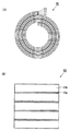
図15(A)は、実施の形態6における超電導コイルを示す概略上面図であり、図15(B)は、実施の形態6における超電導コイルを示す概略正面図である。図15(A)および図15(B)を参照して、本発明の実施の形態6における超電導機器を説明する。本発明の実施の形態6における超電導機器は超電導コイルとしている。実施の形態6における超電導コイル60は、実施の形態1における超電導テープ線材10を用いて巻き形状体が構成されている。
(Embodiment 6)
FIG. 15A is a schematic top view showing the superconducting coil in the sixth embodiment, and FIG. 15B is a schematic front view showing the superconducting coil in the sixth embodiment. With reference to FIG. 15 (A) and FIG. 15 (B), the superconducting apparatus in Embodiment 6 of this invention is demonstrated. The superconducting device in Embodiment 6 of the present invention is a superconducting coil.
詳細には、図15(A)および図15(B)に示すように、超電導コイル60は、テープ状基板11と、中間薄膜層12と、超電導層13とを備えている。超電導層13は、5の領域の超電導層13bに区分するように4列並列に形成された分割領域12aを含んでいる。
Specifically, as shown in FIGS. 15A and 15B, the
そして、分割領域13aが形成された超電導層13と、テープ状基板11を含む超電導テープ線材10が短手方向の一方の辺を軸として、中心を中空としてその周囲を渦巻状に囲むように、超電導テープ線材10が円筒状に巻かれることにより巻き形状体が構成されている。図15では、1つの巻き形状体により超電導コイルが構成されている。
Then, the
次に、実施の形態6における超電導コイルの製造方法について説明する。当該超電導コイルの製造方法は、実施の形態1における超電導テープ線材10を製造する工程(S10〜S40)と、実施の形態3における超電導テープ線材を巻く工程(S60)とを備える。
Next, the manufacturing method of the superconducting coil in Embodiment 6 is demonstrated. The method for manufacturing a superconducting coil includes a step of manufacturing
詳細には、まず、実施の形態1における超電導テープ線材10を製造する工程(S10〜S40)を実施する。
In detail, the process (S10-S40) which manufactures the
次に、巻く工程(S60)を実施する。この工程(S60)では、分割領域13aにより区分された2以上の領域が渦巻状になるように、分割領域13aが形成された超電導テープ線材10を円筒状に巻く。実施の形態6では、超電導テープ線材10を渦巻状に巻くことにより、分割領域13aが渦巻状になるように超電導テープ線材10を円筒状に巻くこととなる。
Next, a winding step (S60) is performed. In this step (S60), the
上記工程(S10,S20,S30,S40,S60)を行なうことにより、実施の形態6における超電導コイルを製造することができる。 By performing the above steps (S10, S20, S30, S40, S60), the superconducting coil in the sixth embodiment can be manufactured.
実施の形態6における超電導コイルの動作は、実施の形態3における超電導コイル40と同様であるので、その説明は繰り返さない。
Since the operation of the superconducting coil in the sixth embodiment is similar to that of
以上説明したように、実施の形態6における超電導機器の一例である超電導コイルの製造方法によれば、巻く工程(S60)において巻き方を渦巻状としている。そのため、所望の形状のコイルに製造することが容易となる。 As described above, according to the method of manufacturing a superconducting coil which is an example of the superconducting device in the sixth embodiment, the winding method is spiral in the winding step (S60). Therefore, it becomes easy to manufacture a coil having a desired shape.
また、実施の形態6における超電導機器の一例である超電導コイルによれば、巻き形状体を渦巻状に円筒状となるように巻くことにより構成されている。そのため、所望の形状のコイルとすることが可能となる。 Moreover, according to the superconducting coil which is an example of the superconducting device in Embodiment 6, it is comprised by winding a winding shape body so that it may become a cylindrical shape spirally. Therefore, it is possible to obtain a coil having a desired shape.
なお、上記実施の形態3〜6は、超電導機器として、超電導コイルを例に挙げて説明したが、特に超電導コイルに限定されない。超電導機器として、たとえば、超電導ケーブル、電力貯蔵装置とすることもできる。また、超電導コイルまたは巻き形状体の断面形状については、円形状の例を示したが、当該断面形状は円形状に限定されず、他の形状(三角形や四角形などの多角形状、あるいは曲面状部と直線状部とを組合せた形状など)であってもよい。 In addition, although the said Embodiment 3-6 demonstrated and demonstrated the superconducting coil as an example as a superconducting apparatus, it is not specifically limited to a superconducting coil. As the superconducting device, for example, a superconducting cable or a power storage device can be used. In addition, as for the cross-sectional shape of the superconducting coil or the wound-shaped body, an example of a circular shape has been shown, but the cross-sectional shape is not limited to a circular shape, and other shapes (polygonal shapes such as triangles and quadrangles, or curved surface portions) And a shape obtained by combining a linear portion and the like.
本発明による超電導機器の製造方法の効果を確認するべく、表1の下段に示す超電導テープ線材を用いて、以下の実施例1および比較例1,2のような、表1上段に示す超電導コイルを製造した。なお、実施例1および比較例1,2の超電導コイルは、1GHzのNMRコイルに適用するものとして製造した。 In order to confirm the effect of the method of manufacturing a superconducting device according to the present invention, the superconducting coil shown in the upper part of Table 1 as in Example 1 and Comparative Examples 1 and 2 below using the superconducting tape wire shown in the lower part of Table 1 Manufactured. The superconducting coils of Example 1 and Comparative Examples 1 and 2 were manufactured to be applied to a 1 GHz NMR coil.
(実施例1における超電導コイルの製造)
実施例1では、実施の形態1の製造方法にしたがって超電導コイルを製造した。具体的には、まず、テープ状基板を準備する工程(S10)を実施した。テープ状基板は、Ni合金系配向テープであるNi−W(タングステン)配向金属テープを用いた。次に、テープ状基板上に中間薄膜層を形成する工程(S20)を実施した。この工程(S20)では、中間薄膜層は、テープ状基板上にRFスパッタ法によりCeO2層を、PLD法によりYSZ層を形成させ、3層構造中間層(CeO/YSZ/CeO2)を形成させた。次に、中間薄膜層上に超電導層を形成する工程(S30)を実施した。この工程(S30)では、超電導層は、中間薄膜層上にPLD法により厚みが約1.0μmのHoBCO膜をエピタキシャル成長させた。
(Manufacture of superconducting coil in Example 1)
In Example 1, a superconducting coil was manufactured according to the manufacturing method of Embodiment 1. Specifically, first, a step of preparing a tape-like substrate (S10) was performed. As the tape-shaped substrate, a Ni-W (tungsten) oriented metal tape that is a Ni alloy-based oriented tape was used. Next, a step (S20) of forming an intermediate thin film layer on the tape-like substrate was performed. In this step (S20), a three-layer structure intermediate layer (CeO / YSZ / CeO 2 ) is formed by forming a CeO 2 layer by RF sputtering and a YSZ layer by PLD on the tape-like substrate. I let you. Next, a step (S30) of forming a superconducting layer on the intermediate thin film layer was performed. In this step (S30), a HoBCO film having a thickness of about 1.0 μm was epitaxially grown on the intermediate thin film layer by the PLD method in the superconducting layer.
この超電導テープ線材は、膜厚が1μmのときJc(臨界電流密度)=1MA/cm2(77K,0T)と仮定すると、Ic(77K,0T)=100Aとなり、1GHzのNMRコイルでの適用条件である温度が4.2K,磁束密度が25Tの磁場環境下では、Ic(4.2K,25T)=1000Aに相当する。 Assuming that Jc (critical current density) = 1 MA / cm 2 (77K, 0T) when the film thickness is 1 μm, this superconducting tape wire has Ic (77K, 0T) = 100 A. Applicable conditions for a 1 GHz NMR coil In a magnetic field environment where the temperature is 4.2 K and the magnetic flux density is 25 T, this corresponds to Ic (4.2 K, 25 T) = 1000 A.
また、超電導層上に5μmの銀からなる膜と20μmの銅めっきを形成した超電導テープ線材は、厚みが0.1mmで幅が5cmである幅広の寸法とした。 Also, the superconducting tape wire in which a film made of 5 μm silver and 20 μm copper plating was formed on the superconducting layer had a width of 0.1 mm and a width of 5 cm.
次に、加工工程(S40)を実施した。この工程(S40)では、超電導層において、連続的にYAGレーザを照射することにより、長手方向に1cm幅の領域を5つ区分するように分割領域を4列並列に形成した。 Next, the processing step (S40) was performed. In this step (S40), the superconducting layer was continuously irradiated with a YAG laser to form four rows of divided regions in parallel so as to divide five 1 cm wide regions in the longitudinal direction.
次に、巻く工程(S60)を実施した。この工程(S60)では、分割領域により区分された4の領域がらせん状になるように、超電導テープ線材を円筒状に巻いた。コイルを20層積層・接続することにより、1GHzのNMRコイルとすることができる。これにより、実施例1における超電導コイルを製造した。 Next, the winding process (S60) was implemented. In this step (S60), the superconducting tape wire was wound in a cylindrical shape so that the four regions divided by the divided regions were spiral. By stacking and connecting 20 layers of coils, a 1 GHz NMR coil can be obtained. Thereby, the superconducting coil in Example 1 was manufactured.
(比較例1における超電導コイルの製造)
比較例1では、径が2.0mmのBi−2212丸線を用いて、14層の超電導コイルを製造した。ここで、Bi−2212とは、ビスマスと鉛とストロンチウムとカルシウムと銅と酸素とを含み、その原子比(酸素を除く)として(ビスマスと鉛):ストロンチウム:カルシウム:銅が2:2:1:2と近似して表わされるBi−Sr−Ca−Cu−O系の酸化物超電導のことである((Bi,Pb)2212と記すこともある)。より具体的には、(BiPb)2Sr2Ca1Cu2O8+Zという化学式で示されるものが含まれる。式中zは、酸素含有量を示し、zが変化することで臨界温度(Tc)や臨界電流(Ic)が変化することが知られている。
(Manufacture of superconducting coil in Comparative Example 1)
In Comparative Example 1, a 14-layer superconducting coil was manufactured using a Bi-2212 round wire having a diameter of 2.0 mm. Here, Bi-2212 includes bismuth, lead, strontium, calcium, copper and oxygen, and the atomic ratio (excluding oxygen) is (bismuth and lead): strontium: calcium: copper is 2: 2: 1. : Bi-Sr-Ca-Cu-O-based oxide superconductivity represented by approximation to 2 (sometimes referred to as (Bi, Pb) 2212). More specifically, those represented by the chemical formula (BiPb) 2 Sr 2 Ca 1 Cu 2 O 8 + Z are included. In the formula, z represents the oxygen content, and it is known that the critical temperature (Tc) and the critical current (Ic) change as z changes.
(比較例2における超電導コイルの製造)
比較例2では、超電導テープ線材の幅が1cmのものを用いた点を除き、実施例1の製造方法における工程(S10〜S30)と同様の工程を実施した。
(Manufacture of superconducting coil in Comparative Example 2)
In Comparative Example 2, the same steps as the steps (S10 to S30) in the manufacturing method of Example 1 were performed except that a superconducting tape wire having a width of 1 cm was used.
次に、加工工程(S40)を行なわずに、巻く工程(S60)を実施した。これにより、比較例2における20層の超電導コイルを製造した。 Next, the winding step (S60) was performed without performing the processing step (S40). Thus, a 20-layer superconducting coil in Comparative Example 2 was manufactured.
(評価結果)
表1に示すように、実施例1における超電導コイルは、1層あたり10mという短い単長の超電導テープ線材により製造することができた。また、加工工程(S20)により1cmの幅に区分された領域の超電導層に、それぞれ160Aの電流を流して通電すると、5の領域それぞれの合計で800Aの通電電流となった。
(Evaluation results)
As shown in Table 1, the superconducting coil in Example 1 could be manufactured with a single-length superconducting tape wire as short as 10 m per layer. In addition, when a current of 160 A was passed through the superconducting layer in the region divided into a width of 1 cm by the processing step (S20), a current of 800 A was obtained in total for each of the five regions.
さらに、超電導層への要求仕様が低くなったため、実施例1における超電導コイルを製造するコストを低減することもできた。 Furthermore, since the required specification for the superconducting layer has been lowered, the cost for producing the superconducting coil in Example 1 could be reduced.
なお、この通電は、1cm幅に区分された5の領域に5個の電源による並列通電を実施した他、シリーズに接続(5の領域を直列に接続)して1個の電源による直列通電を実施した。その結果、いずれの場合においても800Aの通電が可能であった。 In addition, this energization was conducted by parallel energization with 5 power supplies in 5 areas divided into 1 cm width, and connected in series (5 areas connected in series) to conduct series energization with 1 power supply. Carried out. As a result, 800 A energization was possible in any case.
一方、比較例1における超電導コイルは、丸線形状のBi系線材を用いているので、単長が1600mという非常に長い線材が必要となった。 On the other hand, since the superconducting coil in Comparative Example 1 uses a round wire-shaped Bi-based wire, a very long wire having a single length of 1600 m is required.
また、比較例2では、1cm幅テープ形状のHoBCO膜を用いているので、比較例1で必要となった線材の長さよりは短いものの、単長が500mという長い線材が必要となった。 Further, in Comparative Example 2, a 1 cm wide tape-shaped HoBCO film was used, so a long wire having a single length of 500 m was required although it was shorter than the length of the wire required in Comparative Example 1.
(実施例2における超電導コイルの製造)
実施例2では、実施の形態2の製造方法にしたがって超電導コイルを製造した。具体的には、実施例2における超電導コイルは、テープ状基板を準備する工程(S10)、テープ状基板上に中間薄膜層を形成する工程(S20)を実施した。この工程(S10,20)では、実施例1と同様のテープ状基板および中間薄膜層を用いた。
(Manufacture of superconducting coil in Example 2)
In Example 2, a superconducting coil was manufactured according to the manufacturing method of Embodiment 2. Specifically, the superconducting coil in Example 2 performed a step of preparing a tape-shaped substrate (S10) and a step of forming an intermediate thin film layer on the tape-shaped substrate (S20). In this step (S10, 20), the same tape-like substrate and intermediate thin film layer as in Example 1 were used.
次に、中間薄膜層は一方端部から他方端部まで伸び、中間薄膜層に一方端部から他方端部まで延在する少なくとも1つの中間層分割領域を形成する加工工程(S50)を実施した。この工程(S50)では、中間薄膜層にYAGレーザを照射して中間層分割領域を形成した。 Next, the intermediate thin film layer was extended from one end to the other end, and a processing step (S50) for forming at least one intermediate layer division region extending from the one end to the other end in the intermediate thin film layer was performed. . In this step (S50), the intermediate thin film layer was irradiated with a YAG laser to form an intermediate layer divided region.
次に、超電導層を形成する工程(S30)を実施した。この工程(S30)では、中間層分割領域が形成された中間薄膜層上に、実施例1と同様に超電導層を形成した。 Next, a step (S30) of forming a superconducting layer was performed. In this step (S30), a superconducting layer was formed in the same manner as in Example 1 on the intermediate thin film layer in which the intermediate layer division region was formed.
次に、超電導テープ線材を巻く工程(S60)を実施した。これにより、下記の表2に示す実施例2における1層の超電導コイルを製造した。 Next, the process (S60) of winding a superconducting tape wire was carried out. Thus, a one-layer superconducting coil in Example 2 shown in Table 2 below was manufactured.
(実施例3における超電導コイルの製造)
実施例3における超電導コイルは、実施例1で用いた超電導テープ線材を用いて、下記の表2に示す1層の超電導コイルを製造した。
(Manufacture of superconducting coil in Example 3)
For the superconducting coil in Example 3, the superconducting coil of one layer shown in Table 2 below was manufactured using the superconducting tape wire used in Example 1.
(評価結果)
実施例2における超電導コイルに用いている超電導テープ線材において、YAGレーザの照射により中間層分割領域は結晶性を乱れた状態とした。そのため、中間層分割領域上の超電導層は、アモルファス化、または面内の結晶性が不十分であるので、超電導状態とならなかった。そのため、実施例2における超電導コイルに通電させると、中間層分割領域以外の部分の中間薄膜層上の超電導層が超電導状態となるとき、中間薄膜層のうち中間層分割領域となるべき部分上の超電導層が超電導状態とならなかった。
(Evaluation results)
In the superconducting tape wire used for the superconducting coil in Example 2, the crystallinity of the intermediate layer divided region was disturbed by the YAG laser irradiation. For this reason, the superconducting layer on the intermediate layer division region has not been made into a superconducting state because it is amorphized or has insufficient in-plane crystallinity. Therefore, when the superconducting coil in Example 2 is energized, when the superconducting layer on the intermediate thin film layer other than the intermediate layer division region is in the superconducting state, the intermediate thin film layer on the portion to be the intermediate layer division region The superconducting layer was not in the superconducting state.
また、表2に示すように、実施例2(実施の形態2によって製作された超電導テープ線材)によって製作された超電導コイルの性能は実施例3(実施の形態1によって製作された超電導テープ線材)によって製作された超電導コイルと同等の性能を示した。よって、本発明の実施の形態2における超電導コイルの製造方法および超電導コイルの効果が確認できた。 Further, as shown in Table 2, the performance of the superconducting coil manufactured in Example 2 (superconducting tape wire manufactured in accordance with Embodiment 2) is that of Example 3 (superconducting tape wire manufactured in accordance with Embodiment 1). It showed the same performance as the superconducting coil manufactured by. Therefore, the superconducting coil manufacturing method and the effect of the superconducting coil in Embodiment 2 of the present invention were confirmed.
今回開示された実施の形態および実施例はすべての点で例示であって制限的なものではないと考えられるべきである。本発明の範囲は上記した実施の形態ではなくて特許請求の範囲によって示され、特許請求の範囲と均等の意味および範囲内でのすべての変更が含まれることが意図される。 It should be understood that the embodiments and examples disclosed herein are illustrative and non-restrictive in every respect. The scope of the present invention is shown not by the above-described embodiment but by the scope of claims, and is intended to include all modifications within the meaning and scope equivalent to the scope of claims.
10,20,30 超電導テープ線材、11,31 テープ状基板、13,13b,33,33b,52,52b 超電導層、13a,53a 分割領域、13c,32c 一方端部、13d,32d 他方端部、13B 領域、22,32,32b 中間薄膜層、30,40,60 超電導コイル、32a 中間層分割領域、33a 超電導層領域、41a 境界線、41,42,43 巻き形状体。 10, 20, 30 Superconducting tape wire, 11, 31 Tape substrate, 13, 13b, 33, 33b, 52, 52b Superconducting layer, 13a, 53a Divided region, 13c, 32c One end, 13d, 32d The other end, 13B region, 22, 32, 32b intermediate thin film layer, 30, 40, 60 superconducting coil, 32a intermediate layer division region, 33a superconducting layer region, 41a boundary line, 41, 42, 43 wound shape.
Claims (4)
前記テープ状基板上に中間薄膜層を形成する工程と、
前記中間薄膜層は一方端部から他方端部まで伸び、前記中間薄膜層に前記一方端部から前記他方端部まで延在する少なくとも1つの中間層分割領域を形成する加工工程と、
前記中間薄膜層上に超電導層を形成する工程とを備え、
前記中間層分割領域上の超電導層領域は、前記超電導層の臨界温度では超電導状態とならない領域であることを特徴とする、超電導テープ線材の製造方法。 A step of preparing a tape substrate;
Forming an intermediate thin film layer on the tape-shaped substrate;
The intermediate thin film layer extends from one end to the other end, and the intermediate thin film layer forms at least one intermediate layer division region extending from the one end to the other end; and
Forming a superconducting layer on the intermediate thin film layer,
The method of manufacturing a superconducting tape wire, wherein the superconducting layer region on the intermediate layer dividing region is a region that does not become a superconducting state at a critical temperature of the superconducting layer.
前記テープ状基板上に形成された中間薄膜層と、
前記中間薄膜層上に形成され、一方端部から他方端部まで伸び、前記一方端部から前記他方端部まで延在する少なくとも1つの分割領域を含む超電導層とを備え、
前記分割領域は、前記超電導層の臨界温度では超電導状態とならない領域であることを特徴とする、超電導テープ線材。 A tape substrate;
An intermediate thin film layer formed on the tape substrate;
A superconducting layer formed on the intermediate thin film layer, extending from one end to the other end and including at least one divided region extending from the one end to the other end;
The superconducting tape wire according to claim 1, wherein the divided region is a region that is not in a superconducting state at a critical temperature of the superconducting layer.
前記テープ状基板上に形成され、一方端部から他方端部まで伸び、前記一方端部から前記他方端部まで延在する少なくとも1つの中間層分割領域を含む中間薄膜層と、
前記中間薄膜層上に形成された超電導層とを備え、
前記中間層分割領域上の超電導層領域は、前記超電導層の臨界温度では超電導状態とならない領域であることを特徴とする、超電導テープ線材。 A tape substrate;
An intermediate thin film layer formed on the tape-like substrate, extending from one end to the other end and including at least one intermediate layer dividing region extending from the one end to the other end;
A superconducting layer formed on the intermediate thin film layer,
The superconducting tape wire according to claim 1, wherein the superconducting layer region on the intermediate layer dividing region is a region that does not enter a superconducting state at a critical temperature of the superconducting layer.
Priority Applications (1)
| Application Number | Priority Date | Filing Date | Title |
|---|---|---|---|
| JP2012024797A JP2012109263A (en) | 2012-02-08 | 2012-02-08 | Manufacturing method of superconducting tape wire rod, superconducting tape wire rod, and superconducting apparatus |
Applications Claiming Priority (1)
| Application Number | Priority Date | Filing Date | Title |
|---|---|---|---|
| JP2012024797A JP2012109263A (en) | 2012-02-08 | 2012-02-08 | Manufacturing method of superconducting tape wire rod, superconducting tape wire rod, and superconducting apparatus |
Related Parent Applications (1)
| Application Number | Title | Priority Date | Filing Date |
|---|---|---|---|
| JP2005274235A Division JP4984466B2 (en) | 2005-09-21 | 2005-09-21 | Superconducting tape wire manufacturing method |
Publications (1)
| Publication Number | Publication Date |
|---|---|
| JP2012109263A true JP2012109263A (en) | 2012-06-07 |
Family
ID=46494604
Family Applications (1)
| Application Number | Title | Priority Date | Filing Date |
|---|---|---|---|
| JP2012024797A Pending JP2012109263A (en) | 2012-02-08 | 2012-02-08 | Manufacturing method of superconducting tape wire rod, superconducting tape wire rod, and superconducting apparatus |
Country Status (1)
| Country | Link |
|---|---|
| JP (1) | JP2012109263A (en) |
Citations (6)
| Publication number | Priority date | Publication date | Assignee | Title |
|---|---|---|---|---|
| JPS63207007A (en) * | 1987-02-24 | 1988-08-26 | Semiconductor Energy Lab Co Ltd | Superconductor |
| JPH0195576A (en) * | 1987-10-07 | 1989-04-13 | Matsushita Electric Ind Co Ltd | Method for manufacturing thin film superconducting elements |
| JPH01114084A (en) * | 1987-10-28 | 1989-05-02 | Hitachi Ltd | Method of forming superconductor pattern |
| JPH02265283A (en) * | 1989-04-06 | 1990-10-30 | Sanyo Electric Co Ltd | Formation of superconducting circuit |
| JPH03222212A (en) * | 1990-01-29 | 1991-10-01 | Central Res Inst Of Electric Power Ind | Manufacture of high-temperature superconducting wire-rod |
| JP2005079350A (en) * | 2003-08-29 | 2005-03-24 | Japan Science & Technology Agency | High critical current superconductive element |
-
2012
- 2012-02-08 JP JP2012024797A patent/JP2012109263A/en active Pending
Patent Citations (6)
| Publication number | Priority date | Publication date | Assignee | Title |
|---|---|---|---|---|
| JPS63207007A (en) * | 1987-02-24 | 1988-08-26 | Semiconductor Energy Lab Co Ltd | Superconductor |
| JPH0195576A (en) * | 1987-10-07 | 1989-04-13 | Matsushita Electric Ind Co Ltd | Method for manufacturing thin film superconducting elements |
| JPH01114084A (en) * | 1987-10-28 | 1989-05-02 | Hitachi Ltd | Method of forming superconductor pattern |
| JPH02265283A (en) * | 1989-04-06 | 1990-10-30 | Sanyo Electric Co Ltd | Formation of superconducting circuit |
| JPH03222212A (en) * | 1990-01-29 | 1991-10-01 | Central Res Inst Of Electric Power Ind | Manufacture of high-temperature superconducting wire-rod |
| JP2005079350A (en) * | 2003-08-29 | 2005-03-24 | Japan Science & Technology Agency | High critical current superconductive element |
Similar Documents
| Publication | Publication Date | Title |
|---|---|---|
| JP4984466B2 (en) | Superconducting tape wire manufacturing method | |
| JP5806302B2 (en) | Multifilament superconductor with reduced AC loss and its formation method | |
| KR101451599B1 (en) | Superconducting article and manufacturing method | |
| JP6725001B2 (en) | Superconducting wire and superconducting coil | |
| EP2495735A1 (en) | Low ac-loss multi-filament type superconductive wire material, and manufacturing method thereof | |
| JP6364495B2 (en) | Permanent current switch and superconducting coil | |
| EP3474296A1 (en) | Oxide superconducting wire and method for manufacturing same | |
| KR20150065694A (en) | Superconductive coil device and production method | |
| EP2284918A1 (en) | High temperature superconductor, in particular improved coated conductor | |
| JP2016039289A (en) | High temperature superconducting coil and high temperature superconducting magnet device | |
| JP2002150855A (en) | Oxide superconducting wire and manufacturing method thereof | |
| KR20150026820A (en) | Superconductor coil arrangement | |
| JP6507173B2 (en) | Integrated superconductor device and method for manufacturing the same | |
| JP2011076750A (en) | Oxide superconducting cable and method of manufacturing the same | |
| JP2012109263A (en) | Manufacturing method of superconducting tape wire rod, superconducting tape wire rod, and superconducting apparatus | |
| JP6729303B2 (en) | Superconducting wire and superconducting coil | |
| JP2012064495A (en) | Method of producing coated superconducting wire rod, electrodeposition method of superconducting wire rod, and coated superconducting wire rod | |
| JP5614831B2 (en) | Oxide superconducting current lead | |
| JP2012089455A (en) | Manufacturing method of superconducting wire rod and superconducting wire rod | |
| HK1107871B (en) | Method of manufacturing superconducting tape wire, superconducting tape wire, and superconducting apparatus | |
| JP6404556B2 (en) | Oxide superconducting conductor and manufacturing method thereof | |
| JP2009110668A (en) | Superconducting wire and superconducting conductor | |
| JP2008282566A (en) | Bismuth-based oxide superconducting wire, bismuth-based oxide superconducting conductor, superconducting coil, and manufacturing method thereof | |
| JP5986871B2 (en) | Oxide superconducting conductor and manufacturing method thereof | |
| JP2018106839A (en) | Oxide superconducting wire and method for producing the same |
Legal Events
| Date | Code | Title | Description |
|---|---|---|---|
| A621 | Written request for application examination |
Free format text: JAPANESE INTERMEDIATE CODE: A621 Effective date: 20120228 |
|
| A131 | Notification of reasons for refusal |
Free format text: JAPANESE INTERMEDIATE CODE: A131 Effective date: 20130903 |
|
| A521 | Written amendment |
Free format text: JAPANESE INTERMEDIATE CODE: A523 Effective date: 20131022 |
|
| A02 | Decision of refusal |
Free format text: JAPANESE INTERMEDIATE CODE: A02 Effective date: 20131203 |