JP2012113865A - イオンミリング装置及びイオンミリング加工方法 - Google Patents
イオンミリング装置及びイオンミリング加工方法 Download PDFInfo
- Publication number
- JP2012113865A JP2012113865A JP2010260134A JP2010260134A JP2012113865A JP 2012113865 A JP2012113865 A JP 2012113865A JP 2010260134 A JP2010260134 A JP 2010260134A JP 2010260134 A JP2010260134 A JP 2010260134A JP 2012113865 A JP2012113865 A JP 2012113865A
- Authority
- JP
- Japan
- Prior art keywords
- sample
- ion beam
- tilt
- axis
- optical axis
- Prior art date
- Legal status (The legal status is an assumption and is not a legal conclusion. Google has not performed a legal analysis and makes no representation as to the accuracy of the status listed.)
- Granted
Links
Images


Classifications
-
- H—ELECTRICITY
- H01—ELECTRIC ELEMENTS
- H01J—ELECTRIC DISCHARGE TUBES OR DISCHARGE LAMPS
- H01J37/00—Discharge tubes with provision for introducing objects or material to be exposed to the discharge, e.g. for the purpose of examination or processing thereof
- H01J37/30—Electron-beam or ion-beam tubes for localised treatment of objects
- H01J37/305—Electron-beam or ion-beam tubes for localised treatment of objects for casting, melting, evaporating, or etching
- H01J37/3053—Electron-beam or ion-beam tubes for localised treatment of objects for casting, melting, evaporating, or etching for evaporating or etching
-
- H—ELECTRICITY
- H01—ELECTRIC ELEMENTS
- H01J—ELECTRIC DISCHARGE TUBES OR DISCHARGE LAMPS
- H01J37/00—Discharge tubes with provision for introducing objects or material to be exposed to the discharge, e.g. for the purpose of examination or processing thereof
- H01J37/02—Details
- H01J37/20—Means for supporting or positioning the object or the material; Means for adjusting diaphragms or lenses associated with the support
-
- H—ELECTRICITY
- H01—ELECTRIC ELEMENTS
- H01J—ELECTRIC DISCHARGE TUBES OR DISCHARGE LAMPS
- H01J2237/00—Discharge tubes exposing object to beam, e.g. for analysis treatment, etching, imaging
- H01J2237/20—Positioning, supporting, modifying or maintaining the physical state of objects being observed or treated
- H01J2237/2001—Maintaining constant desired temperature
-
- H—ELECTRICITY
- H01—ELECTRIC ELEMENTS
- H01J—ELECTRIC DISCHARGE TUBES OR DISCHARGE LAMPS
- H01J2237/00—Discharge tubes exposing object to beam, e.g. for analysis treatment, etching, imaging
- H01J2237/20—Positioning, supporting, modifying or maintaining the physical state of objects being observed or treated
- H01J2237/202—Movement
- H01J2237/20207—Tilt
-
- H—ELECTRICITY
- H01—ELECTRIC ELEMENTS
- H01J—ELECTRIC DISCHARGE TUBES OR DISCHARGE LAMPS
- H01J2237/00—Discharge tubes exposing object to beam, e.g. for analysis treatment, etching, imaging
- H01J2237/26—Electron or ion microscopes
- H01J2237/28—Scanning microscopes
- H01J2237/2802—Transmission microscopes
-
- H—ELECTRICITY
- H01—ELECTRIC ELEMENTS
- H01J—ELECTRIC DISCHARGE TUBES OR DISCHARGE LAMPS
- H01J2237/00—Discharge tubes exposing object to beam, e.g. for analysis treatment, etching, imaging
- H01J2237/30—Electron or ion beam tubes for processing objects
- H01J2237/317—Processing objects on a microscale
- H01J2237/3174—Etching microareas
- H01J2237/31745—Etching microareas for preparing specimen to be viewed in microscopes or analyzed in microanalysers
Landscapes
- Chemical & Material Sciences (AREA)
- Analytical Chemistry (AREA)
- Physics & Mathematics (AREA)
- Engineering & Computer Science (AREA)
- Plasma & Fusion (AREA)
- Sampling And Sample Adjustment (AREA)
Abstract
【解決手段】イオンビーム2の光軸(Z軸)に対し試料3をチルト振動させて、試料3の加工面3aが傾斜軸方向(Y軸方向)に向いた面状態と、その面状態から加工面3aの試料台側部分が加工面3aのマスク側部分よりも傾斜軸方向(Y軸方向)に突出したチルト面状態との間での、試料3の加工面3aの傾斜及び傾斜回復を繰り返すことにより、加工面3aにイオンビーム2が低角度照射し、ボイド61、異種物質62由来の凹凸63を抑える。
【選択図】図5
Description
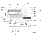
イオンミリング装置1は、真空チャンバ10と、試料3にイオンビーム2を照射するイオンビーム源としてのイオンガン20と、試料3が保持される試料台振動ユニット40を保持する試料ステージ30とを有する。
なお、図2中に記した座標軸において、そのZ軸は、図1に示したイオンガン20から照射されるイオンビーム2の光軸方向若しくはこれと平行な方向を表し、Y軸は、イオンビーム2の光軸に垂直又はほぼ垂直な、試料ステージ30における傾斜ステージ部31の傾斜軸方向若しくはこれと平行な方向を表し、X軸は、イオンビーム2の光軸及び傾斜ステージ部31の傾斜軸に直交する方向を表すものとする。
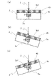
図3は、図2において、試料ステージ駆動機構34の作動によって傾斜ステージ部31が傾斜軸(Y軸)を中心にして揺動している揺動状態における、試料台振動ユニット40の試料3及びマスク45の動きを、傾斜軸方向(Y軸方向)に沿って加工面側から眺めたものである。
図4(a)に示すように、試料3の切削部分にボイド61が生じている場合、試料3をスイングさせながらイオンビーム2を照射して作成した、イオンビーム2の光軸方向(Z軸方向)に沿った試料断面としての目的加工面3a’には、このボイド61の形状に沿って筋状の凹凸63が発生することとなる。同様に、図4(b)に示すように、試料3の切削部分に異種物質62がある場合は、この異種物質62の形状に沿って筋状の凹凸63が発生することとなる。
図5は、試料3のチルト振動状態において、試料3の加工面3aが傾斜軸方向(Y軸方向)に向いた、イオンビーム2の光軸方向(Z軸方向)に沿った面状態に対して、加工面3aの試料台側部分が加工面3aのマスク側部分よりも傾斜軸方向に突出したチルト面状態を示す。
図6に示すように、試料3のチルト状態では、試料台振動ユニット40の試料3を前述のようにスイングさせながらイオンビーム2を照射して作成した加工面3aは、イオンビーム2が低角度照射されるのに対し、加工面3aに発生した筋状の凹凸63の凸部側面63cには、イオンビーム2が加工面3aよりも高角で照射される。これにより、加工面3aのイオンビーム2のスパッタリングによるミリングレートは、筋状の凹凸63の側面63cのイオンビーム2のスパッタリングによるミリングレートよりも大幅に小さくなる。これにより、試料3のチルト状態では、筋状の凹凸63を除去して加工面3aを平滑化する、いわゆるフラットミリングが行える。
図7は、イオンミリング装置1の試料台制御部35が制御するイオンミリング加工方法の制御手順を、時系列的に説明した図である。
11 排気口、 12 真空排気系、 13 真空排気系制御部、
14 試料搬送口、 20 イオンガン(イオンビーム源)、
21 イオンガン制御部、 30 試料ステージ、 31 傾斜ステージ部、
32 蓋体部、 33 ユニット保持部、 34 試料ステージ駆動機構、
35 試料台制御部、 36 ストッパ部、 37 軸着部、 38 凹部、
39 バネ部材、 40 試料台振動ユニット、 41 マスクユニット部、
42 試料台、 43 試料搭載面、 45 マスク、 46 可動部、
45 振動体、 46 稼動部、 47 可動台、 48 搭載面、 49 軸部、
50 振動体(振動モータ)、 61 ボイド、 62 異種物質、
63 筋状の凹凸。
Claims (6)
- イオンビーム源から照射されるイオンビームの光軸に対して垂直又はほぼ垂直な傾斜軸を中心に試料台を揺動させて、該試料台に保持され、マスクによって一部がイオンビームから遮蔽された試料の加工面を、イオンビームの光軸と傾斜軸とにより規定される面に垂直な面に沿って揺動させるスイング機構を備えたイオンミリング装置であって、
前記試料台に保持された試料を、イオンビームの光軸と前記傾斜軸とにより規定される面に垂直な軸を中心に、当該試料の加工面が傾斜軸方向に向いた、イオンビームの光軸方向に沿った面状態と、当該試料の加工面がイオンビームの光軸方向に前記イオンビーム源側に向けて傾斜した、イオンビームの光軸が低角度で交叉する面状態との間で、イオンビームの光軸と傾斜軸とにより規定される面に沿って揺動させるチルト振動機構を備えたことを特徴とするイオンミリング装置。 - 前記チルト振動機構には、イオンビームの光軸に対して前記試料の加工面を交叉させる低角度を変更する設定手段が備えられていることを特徴とする請求項1記載のイオンミリング装置。
- 前記チルト振動機構には、前記試料の加工面の前記マスク側が前記試料台側に対して前記傾斜軸方向に突出するように揺動するのを規制するストッパ部が備えられていることを特徴とする請求項1記載のイオンミリング装置。
- イオンビーム源から照射されるイオンビームの光軸に対して垂直又はほぼ垂直な傾斜軸を中心に試料台を揺動させて、該試料台に保持され、マスクによって一部がイオンビームから遮蔽された試料の加工面を、イオンビームの光軸と傾斜軸とにより規定される面に垂直な面に沿って揺動させながら、前記マスクによって規定された、イオンビームの光軸に沿った試料の加工面を作成する断面作成工程、
前記試料台に保持された試料を、イオンビームの光軸と前記傾斜軸とにより規定される面に垂直な軸を中心に、当該試料の加工面が傾斜軸方向に向いた、イオンビームの光軸方向に沿った面状態と、当該試料の加工面がイオンビームの光軸方向に前記イオンビーム源側に向けて傾斜した、イオンビームの光軸が低角度で交叉する面状態との間で、イオンビームの光軸と傾斜軸とにより規定される面に沿って揺動させ、前記断面作成工程の実行によって当該試料の加工面に生じるスジ状の凹凸を平滑にする平滑化工程、を含むことを特徴とするイオンミリング加工方法。 - イオンビームの光軸に対して前記試料の加工面を交叉させる低角度を、加工対象の前記試料の種別に応じて変更する工程をさらに含むことを特徴とする請求項4記載のイオンミリング加工方法。
- 前記断面作成工程の加工後期に、前記平滑化工程を、前記断面作成工程と一緒に実行することを特徴とする請求項4記載のイオンミリング加工方法。
Priority Applications (6)
| Application Number | Priority Date | Filing Date | Title |
|---|---|---|---|
| JP2010260134A JP5480110B2 (ja) | 2010-11-22 | 2010-11-22 | イオンミリング装置及びイオンミリング加工方法 |
| US13/988,506 US9355817B2 (en) | 2010-11-22 | 2011-11-21 | Ion milling device and ion milling processing method |
| DE112011103860.7T DE112011103860B4 (de) | 2010-11-22 | 2011-11-21 | Ionenätzvorrichtung und lonenätzbearbeitungsverfahren |
| PCT/JP2011/076766 WO2012070517A1 (ja) | 2010-11-22 | 2011-11-21 | イオンミリング装置及びイオンミリング加工方法 |
| CN201180054529.6A CN103210467B (zh) | 2010-11-22 | 2011-11-21 | 离子铣削装置以及离子铣削加工方法 |
| KR1020137012996A KR101622813B1 (ko) | 2010-11-22 | 2011-11-21 | 이온 밀링 장치 및 이온 밀링 가공 방법 |
Applications Claiming Priority (1)
| Application Number | Priority Date | Filing Date | Title |
|---|---|---|---|
| JP2010260134A JP5480110B2 (ja) | 2010-11-22 | 2010-11-22 | イオンミリング装置及びイオンミリング加工方法 |
Publications (2)
| Publication Number | Publication Date |
|---|---|
| JP2012113865A true JP2012113865A (ja) | 2012-06-14 |
| JP5480110B2 JP5480110B2 (ja) | 2014-04-23 |
Family
ID=46145859
Family Applications (1)
| Application Number | Title | Priority Date | Filing Date |
|---|---|---|---|
| JP2010260134A Active JP5480110B2 (ja) | 2010-11-22 | 2010-11-22 | イオンミリング装置及びイオンミリング加工方法 |
Country Status (6)
| Country | Link |
|---|---|
| US (1) | US9355817B2 (ja) |
| JP (1) | JP5480110B2 (ja) |
| KR (1) | KR101622813B1 (ja) |
| CN (1) | CN103210467B (ja) |
| DE (1) | DE112011103860B4 (ja) |
| WO (1) | WO2012070517A1 (ja) |
Cited By (6)
| Publication number | Priority date | Publication date | Assignee | Title |
|---|---|---|---|---|
| WO2014055935A1 (en) | 2012-10-05 | 2014-04-10 | Fei Company | Multidimensional structural access |
| WO2014055974A1 (en) * | 2012-10-05 | 2014-04-10 | Fei Company | Method and system for reducing curtaining in charged particle beam sample preparation |
| WO2015003671A3 (en) * | 2013-07-11 | 2015-04-16 | Tescan Orsay Holding, A.S. | Method of specimen processing in an apparatus with two or more particle beams and apparatus for this processing |
| JP2017539046A (ja) * | 2014-10-15 | 2017-12-28 | ジョン アンドリュ ハント | イオンビームの作用特性を決定し、使用し、表示するための方法及び装置 |
| JP2021148491A (ja) * | 2020-03-17 | 2021-09-27 | ポリプラスチックス株式会社 | 複合材料評価方法 |
| WO2023242909A1 (ja) * | 2022-06-13 | 2023-12-21 | 株式会社日立ハイテク | イオンミリング装置、ホルダおよび断面ミリング処理方法 |
Families Citing this family (15)
| Publication number | Priority date | Publication date | Assignee | Title |
|---|---|---|---|---|
| KR101389939B1 (ko) * | 2013-01-21 | 2014-04-30 | 삼성전자주식회사 | 엑스선 영상 장치 |
| CN105264632B (zh) * | 2013-06-10 | 2017-03-08 | 株式会社日立高新技术 | 离子碾磨装置 |
| JP6326352B2 (ja) * | 2014-11-19 | 2018-05-16 | 日本電子株式会社 | 試料ホルダー、試料作製装置、および位置合わせ方法 |
| WO2017051469A1 (ja) * | 2015-09-25 | 2017-03-30 | 株式会社日立ハイテクノロジーズ | イオンミリング装置 |
| US11226273B2 (en) | 2016-02-03 | 2022-01-18 | Hitachi High-Tech Corporation | Sample holder, ion milling apparatus, sample processing method, sample observing method, and sample processing and observing method |
| KR102145816B1 (ko) * | 2016-02-26 | 2020-08-19 | 주식회사 히타치하이테크 | 이온 밀링 장치, 및 이온 밀링 방법 |
| US10832889B2 (en) | 2016-08-09 | 2020-11-10 | Hitachi High-Tech Corporation | Charged particle beam device |
| JP6814303B2 (ja) | 2017-09-15 | 2021-01-13 | 株式会社日立ハイテク | イオンミリング装置 |
| DE102017130797B4 (de) | 2017-12-20 | 2022-06-09 | Leibniz-Institut für Oberflächenmodifizierung e.V. | Verfahren zur Erzeugung eines gewünschten Oberflächenprofils |
| JP6843790B2 (ja) * | 2018-03-13 | 2021-03-17 | 日本電子株式会社 | イオンミリング装置及び試料ホルダー |
| EP3809447A1 (en) * | 2019-10-18 | 2021-04-21 | FEI Company | Method for large-area 3d analysis of samples using glancing incidence fib milling |
| JP7208195B2 (ja) * | 2020-08-14 | 2023-01-18 | 日本電子株式会社 | イオンミリング装置および試料ホルダー |
| CN114823259B (zh) * | 2021-01-19 | 2026-04-21 | 台湾积体电路制造股份有限公司 | 用于对结构加工的机台及方法 |
| US20240120174A1 (en) * | 2021-01-22 | 2024-04-11 | Hitachi High-Tech Corporation | Ion Milling Device |
| JP7562721B2 (ja) * | 2023-01-19 | 2024-10-07 | 日本電子株式会社 | 試料ホルダー、試料ホルダーセット、および試料作製方法 |
Family Cites Families (10)
| Publication number | Priority date | Publication date | Assignee | Title |
|---|---|---|---|---|
| JPS59184442A (ja) * | 1983-04-04 | 1984-10-19 | Internatl Precision Inc | 電子線機器のゴニオメ−タステ−ジ |
| JP2776415B2 (ja) | 1996-04-26 | 1998-07-16 | 日本電気株式会社 | 試料ホルダ及びホルダ固定具 |
| US6828566B2 (en) * | 1997-07-22 | 2004-12-07 | Hitachi Ltd | Method and apparatus for specimen fabrication |
| JP4335497B2 (ja) * | 2002-07-12 | 2009-09-30 | エスアイアイ・ナノテクノロジー株式会社 | イオンビーム装置およびイオンビーム加工方法 |
| JP4557130B2 (ja) | 2003-09-16 | 2010-10-06 | 日本電子株式会社 | 試料作製装置 |
| EP1780764A1 (en) | 2005-11-01 | 2007-05-02 | FEI Company | Stage assembly, particle-optical apparatus comprising such a stage assembly, and method of treating a sample in such an apparatus |
| JP5410286B2 (ja) | 2006-10-20 | 2014-02-05 | エフ・イ−・アイ・カンパニー | S/temのサンプルを作成する方法およびサンプル構造 |
| JP2008204905A (ja) | 2007-02-22 | 2008-09-04 | Hitachi High-Tech Science Systems Corp | イオンミリング装置、及びイオンミリング加工方法 |
| JP4890373B2 (ja) * | 2007-07-19 | 2012-03-07 | 新日本製鐵株式会社 | 試料作製方法 |
| JP2010260134A (ja) | 2009-05-07 | 2010-11-18 | Hitachi Plant Technologies Ltd | 移載機の給電及び信号伝送方法 |
-
2010
- 2010-11-22 JP JP2010260134A patent/JP5480110B2/ja active Active
-
2011
- 2011-11-21 WO PCT/JP2011/076766 patent/WO2012070517A1/ja not_active Ceased
- 2011-11-21 DE DE112011103860.7T patent/DE112011103860B4/de not_active Expired - Fee Related
- 2011-11-21 CN CN201180054529.6A patent/CN103210467B/zh not_active Expired - Fee Related
- 2011-11-21 KR KR1020137012996A patent/KR101622813B1/ko active Active
- 2011-11-21 US US13/988,506 patent/US9355817B2/en active Active
Cited By (15)
| Publication number | Priority date | Publication date | Assignee | Title |
|---|---|---|---|---|
| TWI612551B (zh) * | 2012-10-05 | 2018-01-21 | Fei公司 | 在帶電粒子束樣品的製備減少屏幕效應之方法及系統 |
| WO2014055974A1 (en) * | 2012-10-05 | 2014-04-10 | Fei Company | Method and system for reducing curtaining in charged particle beam sample preparation |
| WO2014055935A1 (en) | 2012-10-05 | 2014-04-10 | Fei Company | Multidimensional structural access |
| CN104685617A (zh) * | 2012-10-05 | 2015-06-03 | Fei公司 | 用于减少带电粒子束样品制备中的幕化的方法和系统 |
| EP2904633A4 (en) * | 2012-10-05 | 2016-03-02 | Fei Co | MULTI-DIMENSIONAL STRUCTURAL ACCESS |
| US10109457B2 (en) | 2013-07-11 | 2018-10-23 | Tescan Orsay Holding, A.S. | Method of specimen processing in an apparatus with two or more particle beams and apparatus for this processing |
| WO2015003671A3 (en) * | 2013-07-11 | 2015-04-16 | Tescan Orsay Holding, A.S. | Method of specimen processing in an apparatus with two or more particle beams and apparatus for this processing |
| US10629412B2 (en) | 2013-07-11 | 2020-04-21 | Tescan Orsay Holding, A.S. | Apparatus with two or more particle beams for processing a specimen |
| TWI648529B (zh) * | 2013-07-11 | 2019-01-21 | 泰思肯 奧賽 控股 公司 | 利用兩個或更多個粒子束在一裝置中的樣品處理的方法以及用於此處理的裝置 |
| JP2017539046A (ja) * | 2014-10-15 | 2017-12-28 | ジョン アンドリュ ハント | イオンビームの作用特性を決定し、使用し、表示するための方法及び装置 |
| JP2021148491A (ja) * | 2020-03-17 | 2021-09-27 | ポリプラスチックス株式会社 | 複合材料評価方法 |
| JP7440309B2 (ja) | 2020-03-17 | 2024-02-28 | ポリプラスチックス株式会社 | 複合材料評価方法 |
| WO2023242909A1 (ja) * | 2022-06-13 | 2023-12-21 | 株式会社日立ハイテク | イオンミリング装置、ホルダおよび断面ミリング処理方法 |
| JPWO2023242909A1 (ja) * | 2022-06-13 | 2023-12-21 | ||
| JP7706021B2 (ja) | 2022-06-13 | 2025-07-10 | 株式会社日立ハイテク | イオンミリング装置、ホルダおよび断面ミリング処理方法 |
Also Published As
| Publication number | Publication date |
|---|---|
| KR20130086046A (ko) | 2013-07-30 |
| DE112011103860B4 (de) | 2022-08-04 |
| US20130240353A1 (en) | 2013-09-19 |
| US9355817B2 (en) | 2016-05-31 |
| DE112011103860T5 (de) | 2013-08-14 |
| WO2012070517A1 (ja) | 2012-05-31 |
| KR101622813B1 (ko) | 2016-05-19 |
| CN103210467B (zh) | 2015-10-14 |
| CN103210467A (zh) | 2013-07-17 |
| JP5480110B2 (ja) | 2014-04-23 |
Similar Documents
| Publication | Publication Date | Title |
|---|---|---|
| JP5480110B2 (ja) | イオンミリング装置及びイオンミリング加工方法 | |
| CN105047511B (zh) | 离子铣削装置 | |
| US20230369010A1 (en) | Ion Milling Device and Ion Milling Method | |
| JP2008204905A (ja) | イオンミリング装置、及びイオンミリング加工方法 | |
| JP6796552B2 (ja) | イオンミリング装置及び試料ホルダー | |
| JP4675701B2 (ja) | イオンミリング装置およびイオンミリング方法 | |
| JP2022020153A (ja) | イオンミリング装置および試料作製方法 | |
| JP2012193962A (ja) | 薄膜試料作製方法 | |
| JPWO2017134764A1 (ja) | 試料ホルダ、イオンミリング装置、試料加工方法、試料観察方法、及び試料加工・観察方法 | |
| JP5331342B2 (ja) | イオンミリング装置 | |
| JP2004299969A (ja) | シリカガラスのスライス方法 | |
| JP6427601B2 (ja) | イオンミリングのマスク位置調整方法、電子顕微鏡およびマスク調整装置 | |
| JP4675860B2 (ja) | イオンミリング装置及びその方法 | |
| JP7770583B2 (ja) | イオンミリング装置、断面ミリング処理方法及び断面ミリングホルダ | |
| JP6831443B2 (ja) | イオンミリング装置、及びイオンミリング方法 | |
| JP2013165002A (ja) | 荷電粒子線装置、試料マスクユニット、および変換部材 | |
| JP4455432B2 (ja) | イオンミリング装置およびイオンミリング方法 | |
| JP2000263255A (ja) | マーキング装置 | |
| JP6828095B2 (ja) | イオンミリング方法 | |
| JP2020194789A (ja) | イオンミリング方法、およびイオンミリング装置 |
Legal Events
| Date | Code | Title | Description |
|---|---|---|---|
| A621 | Written request for application examination |
Free format text: JAPANESE INTERMEDIATE CODE: A621 Effective date: 20130204 |
|
| TRDD | Decision of grant or rejection written | ||
| A01 | Written decision to grant a patent or to grant a registration (utility model) |
Free format text: JAPANESE INTERMEDIATE CODE: A01 Effective date: 20140121 |
|
| A61 | First payment of annual fees (during grant procedure) |
Free format text: JAPANESE INTERMEDIATE CODE: A61 Effective date: 20140213 |
|
| R150 | Certificate of patent or registration of utility model |
Ref document number: 5480110 Country of ref document: JP Free format text: JAPANESE INTERMEDIATE CODE: R150 |
|
| S531 | Written request for registration of change of domicile |
Free format text: JAPANESE INTERMEDIATE CODE: R313531 |
|
| S533 | Written request for registration of change of name |
Free format text: JAPANESE INTERMEDIATE CODE: R313533 |
|
| R350 | Written notification of registration of transfer |
Free format text: JAPANESE INTERMEDIATE CODE: R350 |