JP2012120253A - 電力伝送システム - Google Patents
電力伝送システム Download PDFInfo
- Publication number
- JP2012120253A JP2012120253A JP2010264875A JP2010264875A JP2012120253A JP 2012120253 A JP2012120253 A JP 2012120253A JP 2010264875 A JP2010264875 A JP 2010264875A JP 2010264875 A JP2010264875 A JP 2010264875A JP 2012120253 A JP2012120253 A JP 2012120253A
- Authority
- JP
- Japan
- Prior art keywords
- power transmission
- frequency
- unit
- voltage
- time
- Prior art date
- Legal status (The legal status is an assumption and is not a legal conclusion. Google has not performed a legal analysis and makes no representation as to the accuracy of the status listed.)
- Granted
Links
Images


Classifications
-
- H—ELECTRICITY
- H02—GENERATION; CONVERSION OR DISTRIBUTION OF ELECTRIC POWER
- H02J—ELECTRIC POWER NETWORKS; CIRCUIT ARRANGEMENTS OR SYSTEMS FOR SUPPLYING OR DISTRIBUTING ELECTRIC POWER; SYSTEMS FOR STORING ELECTRIC ENERGY
- H02J50/00—Circuit arrangements or systems for wireless supply or distribution of electric power
- H02J50/10—Circuit arrangements or systems for wireless supply or distribution of electric power using inductive coupling
- H02J50/12—Circuit arrangements or systems for wireless supply or distribution of electric power using inductive coupling of the resonant type
-
- G—PHYSICS
- G11—INFORMATION STORAGE
- G11C—STATIC STORES
- G11C16/00—Erasable programmable read-only memories
- G11C16/02—Erasable programmable read-only memories electrically programmable
- G11C16/04—Erasable programmable read-only memories electrically programmable using variable threshold transistors, e.g. FAMOS
- G11C16/0483—Erasable programmable read-only memories electrically programmable using variable threshold transistors, e.g. FAMOS comprising cells having several storage transistors connected in series
-
- G—PHYSICS
- G11—INFORMATION STORAGE
- G11C—STATIC STORES
- G11C16/00—Erasable programmable read-only memories
- G11C16/02—Erasable programmable read-only memories electrically programmable
- G11C16/06—Auxiliary circuits, e.g. for writing into memory
- G11C16/08—Address circuits; Decoders; Word-line control circuits
-
- G—PHYSICS
- G11—INFORMATION STORAGE
- G11C—STATIC STORES
- G11C16/00—Erasable programmable read-only memories
- G11C16/02—Erasable programmable read-only memories electrically programmable
- G11C16/06—Auxiliary circuits, e.g. for writing into memory
- G11C16/10—Programming or data input circuits
- G11C16/14—Circuits for erasing electrically, e.g. erase voltage switching circuits
- G11C16/16—Circuits for erasing electrically, e.g. erase voltage switching circuits for erasing blocks, e.g. arrays, words, groups
-
- G—PHYSICS
- G11—INFORMATION STORAGE
- G11C—STATIC STORES
- G11C16/00—Erasable programmable read-only memories
- G11C16/02—Erasable programmable read-only memories electrically programmable
- G11C16/06—Auxiliary circuits, e.g. for writing into memory
- G11C16/24—Bit-line control circuits
-
- G—PHYSICS
- G11—INFORMATION STORAGE
- G11C—STATIC STORES
- G11C16/00—Erasable programmable read-only memories
- G11C16/02—Erasable programmable read-only memories electrically programmable
- G11C16/06—Auxiliary circuits, e.g. for writing into memory
- G11C16/26—Sensing or reading circuits; Data output circuits
-
- G—PHYSICS
- G11—INFORMATION STORAGE
- G11C—STATIC STORES
- G11C29/00—Checking stores for correct operation ; Subsequent repair; Testing stores during standby or offline operation
- G11C29/02—Detection or location of defective auxiliary circuits, e.g. defective refresh counters
- G11C29/021—Detection or location of defective auxiliary circuits, e.g. defective refresh counters in voltage or current generators
-
- G—PHYSICS
- G11—INFORMATION STORAGE
- G11C—STATIC STORES
- G11C29/00—Checking stores for correct operation ; Subsequent repair; Testing stores during standby or offline operation
- G11C29/02—Detection or location of defective auxiliary circuits, e.g. defective refresh counters
- G11C29/028—Detection or location of defective auxiliary circuits, e.g. defective refresh counters with adaption or trimming of parameters
-
- G—PHYSICS
- G11—INFORMATION STORAGE
- G11C—STATIC STORES
- G11C29/00—Checking stores for correct operation ; Subsequent repair; Testing stores during standby or offline operation
- G11C29/04—Detection or location of defective memory elements, e.g. cell constructio details, timing of test signals
- G11C29/08—Functional testing, e.g. testing during refresh, power-on self testing [POST] or distributed testing
- G11C29/12—Built-in arrangements for testing, e.g. built-in self testing [BIST] or interconnection details
- G11C29/18—Address generation devices; Devices for accessing memories, e.g. details of addressing circuits
- G11C29/24—Accessing extra cells, e.g. dummy cells or redundant cells
-
- H—ELECTRICITY
- H10—SEMICONDUCTOR DEVICES; ELECTRIC SOLID-STATE DEVICES NOT OTHERWISE PROVIDED FOR
- H10B—ELECTRONIC MEMORY DEVICES
- H10B43/00—EEPROM devices comprising charge-trapping gate insulators
- H10B43/20—EEPROM devices comprising charge-trapping gate insulators characterised by three-dimensional [3D] arrangements, e.g. with cells on different height levels
- H10B43/23—EEPROM devices comprising charge-trapping gate insulators characterised by three-dimensional [3D] arrangements, e.g. with cells on different height levels with source and drain on different levels, e.g. with sloping channels
- H10B43/27—EEPROM devices comprising charge-trapping gate insulators characterised by three-dimensional [3D] arrangements, e.g. with cells on different height levels with source and drain on different levels, e.g. with sloping channels the channels comprising vertical portions, e.g. U-shaped channels
-
- H—ELECTRICITY
- H10—SEMICONDUCTOR DEVICES; ELECTRIC SOLID-STATE DEVICES NOT OTHERWISE PROVIDED FOR
- H10B—ELECTRONIC MEMORY DEVICES
- H10B43/00—EEPROM devices comprising charge-trapping gate insulators
- H10B43/30—EEPROM devices comprising charge-trapping gate insulators characterised by the memory core region
- H10B43/35—EEPROM devices comprising charge-trapping gate insulators characterised by the memory core region with cell select transistors, e.g. NAND
-
- B—PERFORMING OPERATIONS; TRANSPORTING
- B60—VEHICLES IN GENERAL
- B60L—PROPULSION OF ELECTRICALLY-PROPELLED VEHICLES; SUPPLYING ELECTRIC POWER FOR AUXILIARY EQUIPMENT OF ELECTRICALLY-PROPELLED VEHICLES; ELECTRODYNAMIC BRAKE SYSTEMS FOR VEHICLES IN GENERAL; MAGNETIC SUSPENSION OR LEVITATION FOR VEHICLES; MONITORING OPERATING VARIABLES OF ELECTRICALLY-PROPELLED VEHICLES; ELECTRIC SAFETY DEVICES FOR ELECTRICALLY-PROPELLED VEHICLES
- B60L53/00—Methods of charging batteries, specially adapted for electric vehicles; Charging stations or on-board charging equipment therefor; Exchange of energy storage elements in electric vehicles
- B60L53/30—Constructional details of charging stations
- B60L53/35—Means for automatic or assisted adjustment of the relative position of charging devices and vehicles
- B60L53/38—Means for automatic or assisted adjustment of the relative position of charging devices and vehicles specially adapted for charging by inductive energy transfer
-
- G—PHYSICS
- G11—INFORMATION STORAGE
- G11C—STATIC STORES
- G11C16/00—Erasable programmable read-only memories
- G11C16/02—Erasable programmable read-only memories electrically programmable
- G11C16/06—Auxiliary circuits, e.g. for writing into memory
- G11C16/30—Power supply circuits
-
- G—PHYSICS
- G11—INFORMATION STORAGE
- G11C—STATIC STORES
- G11C16/00—Erasable programmable read-only memories
- G11C16/02—Erasable programmable read-only memories electrically programmable
- G11C16/06—Auxiliary circuits, e.g. for writing into memory
- G11C16/32—Timing circuits
-
- G—PHYSICS
- G11—INFORMATION STORAGE
- G11C—STATIC STORES
- G11C2216/00—Indexing scheme relating to G11C16/00 and subgroups, for features not directly covered by these groups
- G11C2216/12—Reading and writing aspects of erasable programmable read-only memories
- G11C2216/16—Flash programming of all the cells in an array, sector or block simultaneously
-
- G—PHYSICS
- G11—INFORMATION STORAGE
- G11C—STATIC STORES
- G11C5/00—Details of stores covered by group G11C11/00
- G11C5/14—Power supply arrangements, e.g. power down, chip selection or deselection, layout of wirings or power grids, or multiple supply levels
- G11C5/145—Applications of charge pumps; Boosted voltage circuits; Clamp circuits therefor
-
- G—PHYSICS
- G11—INFORMATION STORAGE
- G11C—STATIC STORES
- G11C7/00—Arrangements for writing information into, or reading information out from, a digital store
- G11C7/14—Dummy cell management; Sense reference voltage generators
-
- H—ELECTRICITY
- H02—GENERATION; CONVERSION OR DISTRIBUTION OF ELECTRIC POWER
- H02J—ELECTRIC POWER NETWORKS; CIRCUIT ARRANGEMENTS OR SYSTEMS FOR SUPPLYING OR DISTRIBUTING ELECTRIC POWER; SYSTEMS FOR STORING ELECTRIC ENERGY
- H02J2105/00—Networks for supplying or distributing electric power characterised by their spatial reach or by the load
- H02J2105/30—Networks for supplying or distributing electric power characterised by their spatial reach or by the load the load networks being external to vehicles, i.e. exchanging power with vehicles
- H02J2105/33—Networks for supplying or distributing electric power characterised by their spatial reach or by the load the load networks being external to vehicles, i.e. exchanging power with vehicles exchanging power with road vehicles
- H02J2105/37—Networks for supplying or distributing electric power characterised by their spatial reach or by the load the load networks being external to vehicles, i.e. exchanging power with vehicles exchanging power with road vehicles exchanging power with electric vehicles [EV] or with hybrid electric vehicles [HEV]
Landscapes
- Engineering & Computer Science (AREA)
- Computer Networks & Wireless Communication (AREA)
- Power Engineering (AREA)
- Microelectronics & Electronic Packaging (AREA)
- Inverter Devices (AREA)
- Charge And Discharge Circuits For Batteries Or The Like (AREA)
Abstract
【解決手段】本発明の電力伝送システムは、直流電圧を所定の周波数の交流電圧に変換して出力するスイッチング素子(106)と、前記出力された交流電圧が入力される送電アンテナ部(108)と、前記送電アンテナ部に流れる電流を検出する電流検出部(107)と、前記スイッチング素子がオンとされる時刻と、前記電流検出部によって電流ゼロが検出される時刻との差分の時間を計測するタイマー部(110)と、前記タイマー部によって計測される時間に基づいて前記周波数を設定する周波数設定部(110)と、を有することを特徴とする。
【選択図】 図1
Description
て、前記周波数設定部は前記時間が所定値以内でないと判定すると、前記周波数を変更することを特徴とする。
に搭載される受電アンテナ202を位置合わせした上で、電力の送受を行うようにする。車両の受電アンテナ202は、車両の底面部に配されてなるものである。
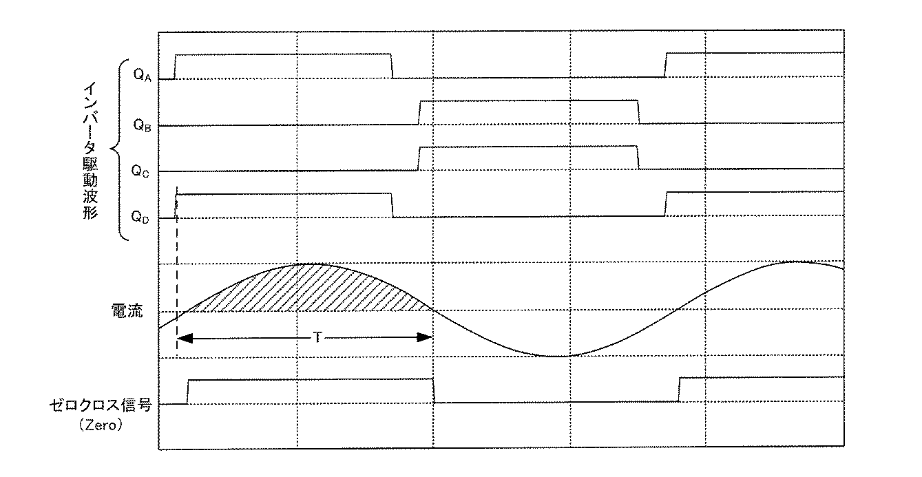
とスイッチング素子QCがオフとされ、スイッチング素子QBとスイッチング素子QCがオ
ンのとき、スイッチング素子QAとスイッチング素子QDがオンとされることで、接続部T1と接続部T2との間に矩形波の交流電圧を発生させる。
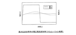
かを判定することで所定の周波数が適切であるか否かを判定する。なお、所定の周波数が適切であるというのは、電力伝送システムの送受電間で伝送効率が最も良くなる周波数を適切であるとして以後も説明する。
至QDそれぞれに対する駆動信号を発生する構成であり、このうちのスイッチング素子QDへの駆動信号はPWM信号として、位相差計測タイマー部115にも入力される。
測タイマー部115が計測したタイマー値はマイクロコンピュータ117側に送信されるようになっている。
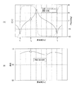
おいては、インピーダンスが極小となる周波数f1、f2によって電力伝送を行ったとしても総合効率上には不利であるので、周波数f0によって電力伝送を行うようにするもので
ある。
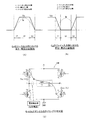
て説明する。図9はスイッチング素子であるFETの損失を説明する図である。以下の説明においては、インバータ部106を構成するスイッチング素子のうちQAとQDがオンとなる半サイクル分のタイミングに基づいて説明するが、スイッチング素子QBとQCがオンとなる半サイクル分についても同様に考えることができる。
示す図であり、図9(B)はスイッチング素子QDのドレイン入力部における電圧・電流
挙動を模式的に示す図であり、図9(C)はスイッチング素子QAとQDがオンとなるタイミングを示す図である。図9(C)においては、スイッチング素子QAとQDがオンとなるときに流れる電流Ipが示されている。
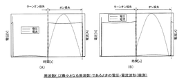
り、図11は極小のインピーダンスを与える周波数f1であるときの電圧・電流波形を示
す図である。図10(A)、図11(A)は図9(A)に相当する実測図であり、図10(B)、図11(B)は図9(B)に相当する実測図である。
高電圧部105で生成する電圧を設定し、ステップS202では、インバータ部106を駆動するための初期周波数の設定を行う。
103・・・発振器
104・・・AC/DC変換部
105・・・高電圧部
106・・・インバータ部
107・・・電流検出部
108・・・送電アンテナ
109・・・低電圧部
110・・・制御部
111・・・交流結合
112・・・比較器
113・・・インバータタイミング発生部
115・・・位相差計測タイマー部
117・・・マイクロコンピュータ
200・・・受電側システム
202・・・受電アンテナ
203・・・整流部
204・・・充電制御部
205・・・バッテリー
Claims (3)
- 直流電圧を所定の周波数の交流電圧に変換して出力するスイッチング素子と、
前記出力された交流電圧が入力される送電アンテナ部と、
前記送電アンテナ部に流れる電流を検出する電流検出部と、
前記スイッチング素子がオンとされる時刻と、前記電流検出部によって電流ゼロが検出される時刻との差分の時間を計測するタイマー部と、
前記タイマー部によって計測される時間に基づいて前記周波数を設定する周波数設定部と、を有することを特徴とする電力伝送システム。 - 前記周波数設定部は前記時間が所定値以内であると判定すると、前記周波数によって電力伝送を行うように決定することを特徴とする請求項1に記載の電力伝送システム。
- 前記周波数設定部は前記時間が所定値以内でないと判定すると、前記周波数を変更することを特徴とする請求項1又は請求項2に記載の電力伝送システム。
Priority Applications (2)
| Application Number | Priority Date | Filing Date | Title |
|---|---|---|---|
| JP2010264875A JP5510670B2 (ja) | 2010-11-29 | 2010-11-29 | 電力伝送システム |
| PCT/JP2011/006602 WO2012073472A1 (ja) | 2010-11-29 | 2011-11-28 | 電力伝送システム |
Applications Claiming Priority (1)
| Application Number | Priority Date | Filing Date | Title |
|---|---|---|---|
| JP2010264875A JP5510670B2 (ja) | 2010-11-29 | 2010-11-29 | 電力伝送システム |
Publications (2)
| Publication Number | Publication Date |
|---|---|
| JP2012120253A true JP2012120253A (ja) | 2012-06-21 |
| JP5510670B2 JP5510670B2 (ja) | 2014-06-04 |
Family
ID=46171446
Family Applications (1)
| Application Number | Title | Priority Date | Filing Date |
|---|---|---|---|
| JP2010264875A Expired - Fee Related JP5510670B2 (ja) | 2010-11-29 | 2010-11-29 | 電力伝送システム |
Country Status (2)
| Country | Link |
|---|---|
| JP (1) | JP5510670B2 (ja) |
| WO (1) | WO2012073472A1 (ja) |
Cited By (4)
| Publication number | Priority date | Publication date | Assignee | Title |
|---|---|---|---|---|
| JP2014124020A (ja) * | 2012-12-20 | 2014-07-03 | Tdk Corp | ワイヤレス電力伝送システム |
| JP2016032345A (ja) * | 2014-07-29 | 2016-03-07 | 日立マクセル株式会社 | 非接触電力伝送装置 |
| JP2016039647A (ja) * | 2014-08-05 | 2016-03-22 | 日立マクセル株式会社 | 非接触電力伝送装置 |
| US10862336B2 (en) | 2015-01-30 | 2020-12-08 | Denso Corporation | Non-contact power-supply device with voltage vector target control |
Citations (3)
| Publication number | Priority date | Publication date | Assignee | Title |
|---|---|---|---|---|
| JP2010114964A (ja) * | 2008-11-04 | 2010-05-20 | Toyota Industries Corp | 非接触電力伝送装置及びその設計方法 |
| JP2010233442A (ja) * | 2009-03-06 | 2010-10-14 | Nissan Motor Co Ltd | 非接触電力供給装置及び方法 |
| JP2011223860A (ja) * | 2010-03-26 | 2011-11-04 | Tdk Corp | ワイヤレス給電装置、ワイヤレス受電装置およびワイヤレス電力伝送システム |
-
2010
- 2010-11-29 JP JP2010264875A patent/JP5510670B2/ja not_active Expired - Fee Related
-
2011
- 2011-11-28 WO PCT/JP2011/006602 patent/WO2012073472A1/ja not_active Ceased
Patent Citations (3)
| Publication number | Priority date | Publication date | Assignee | Title |
|---|---|---|---|---|
| JP2010114964A (ja) * | 2008-11-04 | 2010-05-20 | Toyota Industries Corp | 非接触電力伝送装置及びその設計方法 |
| JP2010233442A (ja) * | 2009-03-06 | 2010-10-14 | Nissan Motor Co Ltd | 非接触電力供給装置及び方法 |
| JP2011223860A (ja) * | 2010-03-26 | 2011-11-04 | Tdk Corp | ワイヤレス給電装置、ワイヤレス受電装置およびワイヤレス電力伝送システム |
Cited By (5)
| Publication number | Priority date | Publication date | Assignee | Title |
|---|---|---|---|---|
| JP2014124020A (ja) * | 2012-12-20 | 2014-07-03 | Tdk Corp | ワイヤレス電力伝送システム |
| JP2016032345A (ja) * | 2014-07-29 | 2016-03-07 | 日立マクセル株式会社 | 非接触電力伝送装置 |
| JP2018183056A (ja) * | 2014-07-29 | 2018-11-15 | マクセルホールディングス株式会社 | 送電装置 |
| JP2016039647A (ja) * | 2014-08-05 | 2016-03-22 | 日立マクセル株式会社 | 非接触電力伝送装置 |
| US10862336B2 (en) | 2015-01-30 | 2020-12-08 | Denso Corporation | Non-contact power-supply device with voltage vector target control |
Also Published As
| Publication number | Publication date |
|---|---|
| JP5510670B2 (ja) | 2014-06-04 |
| WO2012073472A1 (ja) | 2012-06-07 |
Similar Documents
| Publication | Publication Date | Title |
|---|---|---|
| JP5403288B2 (ja) | 電力伝送システム | |
| CN110114958B (zh) | 金属异物检测装置、无线供电装置、无线受电装置及无线电力传输系统 | |
| US10020692B2 (en) | Foreign object detector, power transmitter, power receiver, and wireless power transmission system | |
| JP5177187B2 (ja) | 電力伝送システム | |
| JP5093386B2 (ja) | 送電装置および電力伝送システム | |
| CN110121826B (zh) | 无线供电装置、无线受电装置及无线电力传输系统 | |
| US20130026848A1 (en) | Non-contact power transmission system | |
| JP5770556B2 (ja) | ワイヤレス電力伝送装置および相対位置検出方法 | |
| JP2012217228A (ja) | 電力伝送システム | |
| JP6049669B2 (ja) | 直流電力供給装置および直流電力供給方法 | |
| CN106160253B (zh) | 用于无线功率传输的自由谐振模拟探察 | |
| JP2012175763A (ja) | 非接触電力伝送システム | |
| JP2012110199A (ja) | 電力伝送システム | |
| JP5510670B2 (ja) | 電力伝送システム | |
| JP5761508B2 (ja) | 電力伝送システム | |
| TWI533552B (zh) | 具最大功率追蹤之無線電力傳輸快速充電系統及方法 | |
| JP2012110211A (ja) | 電力伝送システム | |
| EP3009866B1 (en) | Foreign object detector, power transmitter, power receiver, and wireless power transmission system | |
| US10951069B1 (en) | Contactless power supply device and transmitter device | |
| JP5761507B2 (ja) | 電力伝送システム | |
| KR20190020167A (ko) | 송전 장치 및 시스템 | |
| JP2012210116A (ja) | 電力伝送システム | |
| CN119315721A (zh) | 可侦测无线电源接收器与异物的无线电源发射电路及方法 | |
| JP5812264B2 (ja) | 電力伝送システム | |
| CN114448050A (zh) | 无线充电系统的控制方法 |
Legal Events
| Date | Code | Title | Description |
|---|---|---|---|
| A621 | Written request for application examination |
Free format text: JAPANESE INTERMEDIATE CODE: A621 Effective date: 20130328 |
|
| A131 | Notification of reasons for refusal |
Free format text: JAPANESE INTERMEDIATE CODE: A131 Effective date: 20130724 |
|
| A521 | Request for written amendment filed |
Free format text: JAPANESE INTERMEDIATE CODE: A523 Effective date: 20130918 |
|
| TRDD | Decision of grant or rejection written | ||
| A01 | Written decision to grant a patent or to grant a registration (utility model) |
Free format text: JAPANESE INTERMEDIATE CODE: A01 Effective date: 20140226 |
|
| A61 | First payment of annual fees (during grant procedure) |
Free format text: JAPANESE INTERMEDIATE CODE: A61 Effective date: 20140311 |
|
| R150 | Certificate of patent or registration of utility model |
Ref document number: 5510670 Country of ref document: JP Free format text: JAPANESE INTERMEDIATE CODE: R150 |
|
| R250 | Receipt of annual fees |
Free format text: JAPANESE INTERMEDIATE CODE: R250 |
|
| R250 | Receipt of annual fees |
Free format text: JAPANESE INTERMEDIATE CODE: R250 |
|
| R250 | Receipt of annual fees |
Free format text: JAPANESE INTERMEDIATE CODE: R250 |
|
| R250 | Receipt of annual fees |
Free format text: JAPANESE INTERMEDIATE CODE: R250 |
|
| R250 | Receipt of annual fees |
Free format text: JAPANESE INTERMEDIATE CODE: R250 |
|
| LAPS | Cancellation because of no payment of annual fees |