JP2012124149A - Structure for connecting electronic component - Google Patents
Structure for connecting electronic component Download PDFInfo
- Publication number
- JP2012124149A JP2012124149A JP2011180846A JP2011180846A JP2012124149A JP 2012124149 A JP2012124149 A JP 2012124149A JP 2011180846 A JP2011180846 A JP 2011180846A JP 2011180846 A JP2011180846 A JP 2011180846A JP 2012124149 A JP2012124149 A JP 2012124149A
- Authority
- JP
- Japan
- Prior art keywords
- electronic component
- spring pieces
- contact spring
- connection structure
- pair
- Prior art date
- Legal status (The legal status is an assumption and is not a legal conclusion. Google has not performed a legal analysis and makes no representation as to the accuracy of the status listed.)
- Withdrawn
Links
- 239000004065 semiconductor Substances 0.000 claims abstract description 36
- 239000011295 pitch Substances 0.000 abstract description 22
- 238000000034 method Methods 0.000 description 18
- 238000012986 modification Methods 0.000 description 8
- 230000004048 modification Effects 0.000 description 8
- 238000010586 diagram Methods 0.000 description 7
- 238000003780 insertion Methods 0.000 description 4
- 230000037431 insertion Effects 0.000 description 4
- 239000004020 conductor Substances 0.000 description 3
- 210000000078 claw Anatomy 0.000 description 2
- 230000006378 damage Effects 0.000 description 2
- 238000004080 punching Methods 0.000 description 2
- 238000000926 separation method Methods 0.000 description 2
- 230000005611 electricity Effects 0.000 description 1
- 239000002184 metal Substances 0.000 description 1
- 230000003068 static effect Effects 0.000 description 1
Images








Classifications
-
- H—ELECTRICITY
- H01—ELECTRIC ELEMENTS
- H01R—ELECTRICALLY-CONDUCTIVE CONNECTIONS; STRUCTURAL ASSOCIATIONS OF A PLURALITY OF MUTUALLY-INSULATED ELECTRICAL CONNECTING ELEMENTS; COUPLING DEVICES; CURRENT COLLECTORS
- H01R13/00—Details of coupling devices of the kinds covered by groups H01R12/70 or H01R24/00 - H01R33/00
- H01R13/66—Structural association with built-in electrical component
- H01R13/717—Structural association with built-in electrical component with built-in light source
-
- H—ELECTRICITY
- H01—ELECTRIC ELEMENTS
- H01R—ELECTRICALLY-CONDUCTIVE CONNECTIONS; STRUCTURAL ASSOCIATIONS OF A PLURALITY OF MUTUALLY-INSULATED ELECTRICAL CONNECTING ELEMENTS; COUPLING DEVICES; CURRENT COLLECTORS
- H01R13/00—Details of coupling devices of the kinds covered by groups H01R12/70 or H01R24/00 - H01R33/00
- H01R13/02—Contact members
- H01R13/15—Pins, blades or sockets having separate spring member for producing or increasing contact pressure
- H01R13/17—Pins, blades or sockets having separate spring member for producing or increasing contact pressure with spring member on the pin
-
- H—ELECTRICITY
- H01—ELECTRIC ELEMENTS
- H01R—ELECTRICALLY-CONDUCTIVE CONNECTIONS; STRUCTURAL ASSOCIATIONS OF A PLURALITY OF MUTUALLY-INSULATED ELECTRICAL CONNECTING ELEMENTS; COUPLING DEVICES; CURRENT COLLECTORS
- H01R11/00—Individual connecting elements providing two or more spaced connecting locations for conductive members which are, or may be, thereby interconnected, e.g. end pieces for wires or cables supported by the wire or cable and having means for facilitating electrical connection to some other wire, terminal, or conductive member, blocks of binding posts
- H01R11/03—Individual connecting elements providing two or more spaced connecting locations for conductive members which are, or may be, thereby interconnected, e.g. end pieces for wires or cables supported by the wire or cable and having means for facilitating electrical connection to some other wire, terminal, or conductive member, blocks of binding posts characterised by the relationship between the connecting locations
- H01R11/07—Individual connecting elements providing two or more spaced connecting locations for conductive members which are, or may be, thereby interconnected, e.g. end pieces for wires or cables supported by the wire or cable and having means for facilitating electrical connection to some other wire, terminal, or conductive member, blocks of binding posts characterised by the relationship between the connecting locations the connecting locations being of the same type but different sizes
-
- H—ELECTRICITY
- H01—ELECTRIC ELEMENTS
- H01R—ELECTRICALLY-CONDUCTIVE CONNECTIONS; STRUCTURAL ASSOCIATIONS OF A PLURALITY OF MUTUALLY-INSULATED ELECTRICAL CONNECTING ELEMENTS; COUPLING DEVICES; CURRENT COLLECTORS
- H01R12/00—Structural associations of a plurality of mutually-insulated electrical connecting elements, specially adapted for printed circuits, e.g. printed circuit boards [PCB], flat or ribbon cables, or like generally planar structures, e.g. terminal strips, terminal blocks; Coupling devices specially adapted for printed circuits, flat or ribbon cables, or like generally planar structures; Terminals specially adapted for contact with, or insertion into, printed circuits, flat or ribbon cables, or like generally planar structures
- H01R12/70—Coupling devices
- H01R12/71—Coupling devices for rigid printing circuits or like structures
- H01R12/72—Coupling devices for rigid printing circuits or like structures coupling with the edge of the rigid printed circuits or like structures
-
- H—ELECTRICITY
- H01—ELECTRIC ELEMENTS
- H01R—ELECTRICALLY-CONDUCTIVE CONNECTIONS; STRUCTURAL ASSOCIATIONS OF A PLURALITY OF MUTUALLY-INSULATED ELECTRICAL CONNECTING ELEMENTS; COUPLING DEVICES; CURRENT COLLECTORS
- H01R13/00—Details of coupling devices of the kinds covered by groups H01R12/70 or H01R24/00 - H01R33/00
- H01R13/66—Structural association with built-in electrical component
- H01R13/717—Structural association with built-in electrical component with built-in light source
- H01R13/7175—Light emitting diodes (LEDs)
Landscapes
- Physics & Mathematics (AREA)
- Engineering & Computer Science (AREA)
- Microelectronics & Electronic Packaging (AREA)
- Optics & Photonics (AREA)
- Led Device Packages (AREA)
- Connecting Device With Holders (AREA)
- Connection Or Junction Boxes (AREA)
- Details Of Connecting Devices For Male And Female Coupling (AREA)
Abstract
【課題】バスバーを一種類にして、接点間のピッチや外形状、大きさ等が異なる複数種の表面実装用の電子部品を接続できる電子部品の接続構造を提供する。
【解決手段】一端17にそれぞれ端子部19を形成した2本のバスバー13が離間して並列配置され、各端子部19には2種類の電子部品11の各一対の接点部に弾接可能な二対の平行な左右接触バネ片23a,24a,23b,24bが上下2段に配置して形成され、並列配置されたバスバー13の上段における左右接触バネ片23a,24aが2本のバスバー間に配置された半導体発光素子25の一対の接点部21と接続され、並列配置されたバスバー13の下段における左右接触バネ片24b,24bが2本のバスバー間に配置されたツエナーダイオード27の一対の接点部21と接続される。
【選択図】図1Provided is an electronic component connection structure that can connect a plurality of types of surface mounting electronic components with different pitches, outer shapes, sizes, and the like between contact points by using a single bus bar.
Two bus bars 13 each having a terminal portion 19 formed at one end 17 are spaced apart and arranged in parallel, and each terminal portion 19 can be elastically contacted with a pair of contact portions of two types of electronic components 11. Two pairs of parallel left and right contact spring pieces 23a, 24a, 23b, 24b are formed in two upper and lower stages, and the left and right contact spring pieces 23a, 24a in the upper stage of the bus bar 13 arranged in parallel are between the two bus bars. A pair of contacts of a Zener diode 27 in which the left and right contact spring pieces 24b, 24b on the lower stage of the bus bar 13 arranged in parallel are connected between the two bus bars are connected to the pair of contact portions 21 of the arranged semiconductor light emitting elements 25. Connected to the unit 21.
[Selection] Figure 1
Description
本発明は、異なる接点間ピッチの電子部品を接続可能とする電子部品の接続構造に関する。 The present invention relates to an electronic component connection structure that enables connection of electronic components having different pitches between contacts.
電子部品の電気的な接続を確実に行うことで高い信頼性を得る電子部品の接続構造が特許文献1に開示されている。図20に示すように、この電子部品の接続構造は、ハウジングに、一対のバスバー501,503が組み付けられるとともに光源である半導体発光素子(LED)505が組み付けられる。平板形状をなして2分割されたバスバー501,503は、電線接続部507と、ツエナーダイオード接続部509と、抵抗器接続部511と、LED接続部513と、を有する。抵抗器接続部511には、2分割されたバスバー501,503のそれぞれに圧接刃515,515が備えられる。ツエナーダイオード接続部509には、単一の圧接刃517が一方のバスバー501に、単一の圧接刃519が他方のバスバー503に備えられる。
Patent Document 1 discloses a connection structure for an electronic component that obtains high reliability by reliably performing electrical connection of the electronic component. As shown in FIG. 20, in this electronic component connection structure, a pair of
ツエナーダイオード521は、一方のリード部523が一方のバスバー501に、他方のリード部525が他方のバスバー503にそれぞれ電気的に接続されることで、抵抗器527の下流側で一対のバスバー501,503に並列に接続され、ダイオードに順起電力が流れる方向で静電気により回路に印加される突発的な大電圧からのLEDを破壊から保護し、ダイオードに逆起電力が流れる方向では通電を阻止し、同じくLEDを破壊から保護する機能を果たす。
The
しかしながら、従来の電子部品の接続構造は、電子部品の形状、大きさに合わせ異なる寸法の接続部(圧接刃515,515,圧接刃517,圧接刃519)を形成した2種類のバスバー501,503が必要となった。また、リード部を有したスルーホール用の電子部品(ツエナーダイオード521,抵抗器527)しか実装できず、近年需要が多く安価となった表面実装用の電子部品の接続ができない問題があった。
However, the conventional electronic component connection structure has two types of
本発明は上記状況に鑑みてなされたもので、その目的は、バスバーを一種類にして、接点間のピッチや外形状、大きさ等が異なる複数種の表面実装用の電子部品を接続できる電子部品の接続構造を提供することにある。 The present invention has been made in view of the above situation, and an object of the present invention is to provide an electronic device capable of connecting a plurality of types of surface mounting electronic components having different pitches, outer shapes, sizes, and the like between contact points using a single bus bar. It is to provide a connection structure for components.
本発明に係る上記目的は、下記構成により達成される。
(1) 一端にそれぞれ端子部を形成した複数のバスバーが離間して並列配置され、前記各端子部には複数種の電子部品の各一対の接点部に弾接可能な少なくとも二対の平行な左右接触バネ片が多段に配置して形成され、並列配置された前記バスバーの各段における前記左右接触バネ片のうち少なくとも何れか2片が前記バスバー間に配置された複数種の前記電子部品の各一対の前記接点部と接続されることを特徴とする電子部品の接続構造。
The above object of the present invention is achieved by the following configuration.
(1) A plurality of bus bars each having a terminal portion formed at one end thereof are spaced apart and arranged in parallel, and each terminal portion has at least two parallel pairs that can be elastically contacted with each pair of contact portions of a plurality of types of electronic components. The left and right contact spring pieces are arranged in multiple stages, and at least any two of the left and right contact spring pieces in each stage of the bus bars arranged in parallel are arranged between the bus bars. An electronic component connection structure, wherein the electronic component connection structure is connected to each pair of contact portions.
この電子部品の接続構造によれば、少なくとも二対の左右接触バネ片が多段に配置して形成された端子部を有する複数のバスバーが離間して並列配置され、複数のバスバーの各段における左右接触バネ片のうち少なくとも何れか2片が、バスバー間に配置された複数種の電子部品の各一対の接点部と接続される。そこで、並列配置された複数のバスバー間における端子部の各段には、接点間ピッチや外形状、大きさ等の異なる複数種の電子部品が接続可能となる。 According to this electronic component connection structure, a plurality of bus bars having terminal portions formed by arranging at least two pairs of left and right contact spring pieces in multiple stages are spaced apart and arranged in parallel, and left and right in each stage of the plurality of bus bars. At least any two of the contact spring pieces are connected to each pair of contact portions of a plurality of types of electronic components disposed between the bus bars. Therefore, a plurality of types of electronic components having different contact pitches, outer shapes, sizes, and the like can be connected to the respective stages of the terminal portions between the plurality of bus bars arranged in parallel.
(2) (1)の電子部品の接続構造であって、前記バスバーは、略Y字状に分岐した一対の接触バネ片の先端に二対の前記左右接触バネ片を有し、2本の前記バスバーを平行に離間配置することで前記左右接触バネ片の先端部の電気接触部が片側4箇所ずつの8箇所に配置され、一方の段では隣接する前記左右接触バネ片の電気接触部に第1の前記電子部品の一対の接点部が接触し、他方の段では少なくとも1つの電気接触部を跨いで前記左右接触バネ片の電気接触部に第2の前記電子部品の一対の接点部が接触することを特徴とする電子部品の接続構造。 (2) In the connection structure of electronic components according to (1), the bus bar has two pairs of left and right contact spring pieces at the ends of a pair of contact spring pieces branched in a substantially Y shape. By arranging the bus bars apart from each other in parallel, the electrical contact portions at the tip of the left and right contact spring pieces are arranged at 8 locations on each side, and on one stage, the electrical contact portions of the adjacent left and right contact spring pieces are arranged on one side. The pair of contact parts of the first electronic component is in contact with each other, and at the other stage, the pair of contact parts of the second electronic component is placed on the electrical contact part of the left and right contact spring piece across at least one electrical contact part. An electronic component connection structure characterized by contact.
この電子部品の接続構造によれば、略Y字状に分岐した一対の接触バネ片の先端に二対の左右接触バネ片を有するバスバーが、2本平行に離間配置されることで、片側4箇所の電気接触部が両側で8箇所配置される。これにより、一方の段では隣接する左右接触バネ片の電気接触部に接点間ピッチの小さい第1の電子部品の一対の接点部が接続可能となり、他方の段では少なくとも1つの電気接触部を跨いで左右接触バネ片の電気接触部に接点間ピッチの大きい第2の電子部品の一対の接点部が接続可能となる。 According to this electronic component connection structure, two bus bars each having two pairs of left and right contact spring pieces at the tips of a pair of contact spring pieces branched in a substantially Y shape are arranged in parallel on one side 4. Eight electrical contact portions are arranged on both sides. Thereby, in one stage, a pair of contact parts of the first electronic component having a small pitch between the contacts can be connected to the electrical contact parts of the adjacent left and right contact spring pieces, and in the other stage, at least one electrical contact part is straddled. Thus, the pair of contact parts of the second electronic component having a large pitch between the contacts can be connected to the electrical contact parts of the left and right contact spring pieces.
(3) (2)の電子部品の接続構造であって、前記バスバーは、一対の側壁が平行となるようにU字状に折り曲げ形成され、前記側壁のそれぞれに前記接触バネ片が打ち抜き成形されていることを特徴とする電子部品の接続構造。 (3) In the electronic component connection structure according to (2), the bus bar is formed in a U shape so that a pair of side walls are parallel to each other, and the contact spring piece is stamped and formed on each of the side walls. An electronic component connection structure characterized by that.
この電子部品の接続構造によれば、バスバーの本体がU字状に折り曲げられて形成され、その対向する一対の側壁に、打ち抜き加工によって略Y字状に分岐した接触バネ片の先端に二対の左右接触バネ片がそれぞれ形成される。これにより、多数の電気接触部を有する弾接構造が容易且つコンパクトに製造可能となる。 According to this electronic component connection structure, the bus bar body is formed by being bent in a U shape, and two pairs are formed at the ends of the contact spring pieces branched into a substantially Y shape by punching on a pair of opposing side walls. Left and right contact spring pieces are respectively formed. Thereby, the elastic contact structure which has many electrical contact parts can be manufactured easily and compactly.
(4) (1)〜(3)のいずれか1つの電子部品の接続構造であって、前記電子部品の1つが半導体発光素子であり、前記半導体発光素子は、発光部が2本の前記バスバーの間に配置され、前記バスバーの前記発光部を挟むそれぞれの側壁面には反射面が形成されることを特徴とする電子部品の接続構造。 (4) A connection structure of electronic components according to any one of (1) to (3), wherein one of the electronic components is a semiconductor light emitting element, and the semiconductor light emitting element includes the bus bar having two light emitting portions. A connecting structure for electronic parts, characterized in that a reflective surface is formed on each side wall surface that is disposed between and sandwiches the light emitting portion of the bus bar.
この電子部品の接続構造によれば、半導体発光素子の発光部が、平行に離間配置された2本のバスバーの間に挟まれた状態に配置される。発光部を挟む2本のバスバーのそれぞれの側壁が反射面で形成されることにより、発光部から出射される光が反射面で反射して出射の方向に向けられ、出射光の有効利用が可能となる。 According to this electronic component connection structure, the light emitting portion of the semiconductor light emitting element is disposed in a state of being sandwiched between two bus bars spaced apart in parallel. Each side wall of the two bus bars sandwiching the light emitting part is formed by a reflecting surface, so that the light emitted from the light emitting part is reflected by the reflecting surface and directed in the direction of emission, and the emitted light can be used effectively. It becomes.
本発明に係る電子部品の接続構造によれば、バスバーを一種類にして、接点間のピッチや外形状、大きさ等が異なる表面実装用の電子部品を接続することができる。 According to the electronic component connection structure of the present invention, it is possible to connect surface mount electronic components having different pitches, outer shapes, sizes, and the like between the contacts by using one type of bus bar.
以下、本発明の一実施の形態を図面を参照して説明する。
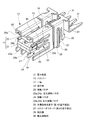
図1は本発明の第1実施形態に係る電子部品の接続構造に用いられる2本のバスバーの斜視図、図2は図1に示したバスバーを収容したハウジングの斜視図である。
本第1実施形態に係る電子部品11の接続構造は、図1に示す2本の同一形状のバスバー13を構成の主要部として有している。この2本のバスバー13は、図2に示すハウジング15に収容されて使用される。
Hereinafter, an embodiment of the present invention will be described with reference to the drawings.
FIG. 1 is a perspective view of two bus bars used in the electronic component connection structure according to the first embodiment of the present invention, and FIG. 2 is a perspective view of a housing that houses the bus bars shown in FIG.
The connection structure of the
2本のバスバー13は、一端17にそれぞれ端子部19を形成し、離間して並列配置される。端子部19は、複数種(本実施形態では2種類)の電子部品11の各一対の接点部21に弾接可能な少なくとも二対の平行な左右接触バネ片23a,24a、23b,24bが上下多段(本実施形態では2段)に配置して形成される。
本実施の形態では、1本のバスバー13に、略Y字状に分岐した一対の接触バネ片23,24の先端に二対の左右接触バネ片23a,24a、23b,24bが設けられる。並列配置されたバスバー13の上段における4つの左右接触バネ片23a,24a,23a,24aのうち隣接する2つの左右接触バネ片24a,23aの電気接触部45が、2本のバスバー13間に配置された第1の電子部品11である半導体発光素子25の一対の接点部21と接続する(図4参照)。また、並列配置されたバスバー13の下段における4つの左右接触バネ片23b,24b,23b,24bのうち1つの左右接触バネ片23bを跨いだ2つの左右接触バネ片24b,24bの電気接触部45が、2本のバスバー13間で半導体発光素子25の下方に位置する第2の電子部品11であるツエナーダイオード27の一対の接点部21と接続する(図4参照)。
The two
In the present embodiment, one
図3は図1に示した1つのバスバー13の斜視図である。
バスバー13は、ハウジング15に装着された状態でその一部分がハウジング15の外部に突出される。本実施の形態において、バスバー13の一部分がハウジング15から突出する側を「後」、その反対側を「前」と称する。バスバー13の後端には被覆された電線の被覆を切り裂き導体と電気的に接触するための圧接刃31が設けられる。圧接刃31の前部には後部当接片33と、後部弾性脚35と、前部弾性脚37と、前部当接片39とが連設される。
FIG. 3 is a perspective view of one
A part of the
図3の背面側の前部当接片39には、バスバー13の一端17(前端)となる端子部19が連結部41(図4(a)参照)を介して連設されている。圧接刃31、後部当接片33、後部弾性脚35、前部弾性脚37、前部当接片39、端子部19は、板金加工により一体に打ち抜かれた後、図3に示す形状に折り曲げ加工される。バスバー13の端子部19は、一対の側壁43が平行となるようにU字状に折り曲げ形成され、側壁43のそれぞれに接触バネ片23,24が打ち抜き成形される。バスバー13の本体がU字状に折り曲げられて形成され、その対向する一対の側壁43に、打ち抜き加工によって略Y字状に分岐した接触バネ片23,24の先端に二対の左右接触バネ片23a,24a、23b,24bが形成されることにより、多数の電気接触部45を有する弾接構造が容易且つコンパクトに製造可能となっている。
A
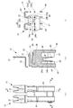
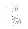
図4(a)は図1に示したバスバー13の平面図、(b)はそのA−A断面矢視図、(c)はそのB−B断面矢視図で、電子部品の装着状態を示した図、図5(a)は半導体発光素子25の斜視図、(b)はツエナーダイオード27の斜視図である。
1本のバスバー13において、一対の接触バネ片23,24は、平行となるように形成され、略Y字状に分岐した各先端に二対の左右接触バネ片23a,24a、23b,24bを有する。各左右接触バネ片23a,24a、23b,24bの先端に突設される電気接触部45は、接点が頂角となる三角形状に形成される。図4(a)に示すように、バスバー13は、2本が平行に離間配置される。これにより、並列配置されたバスバー13の左右接触バネ片23a,24a、23b,24bの先端の電気接触部45は、図4(c)に示すように、片側4箇所ずつの8箇所に配置されることになる。並列配置されたバスバー13の上段における4つの左右接触バネ片23a,24a,23a,24aの上側4箇所の電気接触部45には、それぞれのバスバー13に形成された上方部品座部47が対峙される。また、並列配置されたバスバー13の下段における4つの左右接触バネ片23b,24b,23b,24bの下側4箇所の電気接触部45には、それぞれのバスバー13に形成された下方部品座部49が対峙される。
4A is a plan view of the
In one
上方部品座部47と、上段における4つの左右接触バネ片23a,24a,23a,24aの上側4箇所の電気接触部45との間には、半導体発光素子25が装着されている。下段における4つの左右接触バネ片23b,24b,23b,24bの下側4箇所の電気接触部45と、下方部品座部49との間には、ツエナーダイオード27が装着されている。半導体発光素子25は、図5(a)に示すように、一方の面に、一対の接点部21が設けられた表面実装用の電子部品11となっている。また、ツエナーダイオード27も、図5(b)に示すように、一方の面に一対の接点部21が設けられた表面実装用の電子部品11となっている。
The semiconductor
半導体発光素子25は、図4(c)に示すように、接点部21を設けられた面が、上段の左右接触バネ片23a,24aの電気接触部45に向けられ、背面が上方部品座部47に当接される。ツエナーダイオード27は、接点部21を設けられた面が、下段の左右接触バネ片23b,24bの電気接触部45の側に向けられ、背面が下方部品座部49に当接される。
本実施の形態では、半導体発光素子25の接点間ピッチが、ツエナーダイオード27の接点間ピッチよりも小さい。つまり、2つの電子部品11は、異なる接点間ピッチとなっている。電子部品11の接続構造では、このような異なる接点間ピッチの2種類の電子部品11を同時に実装可能としている。すなわち、図4(c)に示すように、並列配置されたバスバー13の上段における4つの左右接触バネ片23a,24a,23a,24aのうち隣接する2つの左右接触バネ片24a,23aの電気接触部45が半導体発光素子25の一対の接点部21に接触し、並列配置されたバスバー13の下段における4つの左右接触バネ片23b,24b,23b,24bのうち1つの左右接触バネ片23bを跨いだ2つの左右接触バネ片24b,24bの電気接触部45がツエナーダイオード27の一対の接点部21に接触している。
As shown in FIG. 4C, the surface of the semiconductor
In the present embodiment, the pitch between the contacts of the semiconductor
すなわち、図4(c)において、半導体発光素子25は、並列配置されたバスバー13の上段の電気接触部45において、左側から2番目の電気接触部45と、左側から3番目の電気接触部45とに接続される。また、ツエナーダイオード27は、並列配置されたバスバー13の下段の電気接触部45において、左側から1番目の電気接触部45と、左側から3番目の電気接触部45とに接続されるが、左側から2番目の電気接触部45と、左側から4番目の電気接触部45とに接続することもできる。また、本実施の形態において、ツエナーダイオード27は、接点間ピッチが、電気接触部45の接点間ピッチの2倍の距離となるものが用いられているが、接点間ピッチが電気接触部45の接点間ピッチの3倍の距離となるものも用いることができる。この場合、ツエナーダイオード27の一対の接点部21は、左側から1番目の電気接触部45と、左側から4番目の電気接触部45とに接続される。
That is, in FIG. 4C, the semiconductor
次に、上記構成の電子部品11の接続構造の組付け工程を説明する。
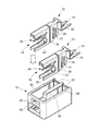
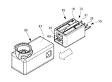
図6は本発明の第1実施形態に係る電子部品11の接続構造におけるバスバー組付け工程図、図7は同様に電子部品組付け工程を説明する図、図8は同様にハウジング組付け工程を説明する図、図9は同様に電線ホルダー組付け工程を説明する図、図10は本発明の第1実施形態に係る電子部品11の接続構造を用いたLEDユニット53の斜視図である。
上記の電子部品11の接続構造は、例えばLEDユニット53に好適に採用することができる。電子部品11の接続構造をLEDユニット53に適用するには、図6に示すように、2本のバスバー13をハウジング15に装着する。
Next, an assembling process of the connection structure of the
FIG. 6 is a bus bar assembly process diagram in the connection structure of the
The connection structure of the
ハウジング15には2つのバスバー収用室55が形成される。バスバー収用室55は、後端が後壁57となり、その前方の内壁面に一対の保持溝59がそれぞれのバスバー収用室55に形成されている。バスバー収用室55に挿入されたバスバー13は、後部当接片33と後部弾性脚35とで後壁57を挟持し、ハウジング15から脱落規制されて装着される。
In the
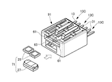
図7に示すように、ハウジング15の前面にはLED装着開口部61と、ダイオード装着開口部63とが上下2段で形成されている。LED装着開口部61には、半導体発光素子25が、接点部21を下側にして挿入される。ダイオード装着開口部63には、ツエナーダイオード27が、接点部21を上側にして挿入される。これにより、それぞれの接点部21が図4(c)に示したように、それぞれの電気接触部45に接続される。また、ハウジング15の底面には抵抗装着開口部(図示せず)が形成されており、抵抗器28が挿入される。これにより、手前のバスバー13における前部当接片39と前部弾性脚37とで抵抗器28を挟持し、前部弾性脚37の電気接触部が抵抗器28の一対の接点部に接続される(図1参照)。
ここで、本実施形態に係るLEDユニット53は、半導体発光素子25及びツエナーダイオード27と、陽極端子及び負極端子との間にそれぞれ抵抗器28を設けた回路とする必要がある。そこで、図7に示すように、手前のバスバー13における一対の前部当接片39及び前部弾性脚37の間に破断部16が形成される。これにより、手前のバスバー13に装着された抵抗器28は、半導体発光素子25及びツエナーダイオード27と直列接続される。
As shown in FIG. 7, an
Here, the
図8に示すように、半導体発光素子25と、ツエナーダイオード27とを装着したハウジング15は、レンズカバー65に装着される。レンズカバー65の後端面にはハウジング挿入開口67が形成されている。レンズカバー65に挿入されたハウジング15は、圧接刃31がレンズカバー65の内部で後方に向かって突出している。
As shown in FIG. 8, the
図9に示すように、ハウジング15を装着したレンズカバー65には電線ホルダー69がハウジング挿入開口67から挿入される。電線ホルダー69の3方の外面にはコ字状の電線保持溝71が2箇所に形成されている。それぞれの電線保持溝71には被覆付き電線29がコ字状に曲げられて装着される。電線ホルダー69の前面にはそれぞれの電線保持溝71を跨って、水平な圧接刃進入スリット73が形成されている。これにより、電線ホルダー69がレンズカバー65に挿入されると、レンズカバー65の内部で後方に向かって突出したバスバー13の圧接刃31が、圧接刃進入スリット73に進入し、圧接刃31と電線29の導体とが接続されるようになされている。
As shown in FIG. 9, the
レンズカバー65に挿入された電線ホルダー69は、レンズカバー65の側部に形成さける係止穴75に、側面に突設した係止爪77を係止して、レンズカバー65からのハウジング15と、電線ホルダー69自身との離脱が規制される。レンズカバー65に、ハウジング15、電線ホルダー69が装着されることで図10に示すLEDユニット53が構成される。
The
このように、本第1実施形態の電子部品11の接続構造では、二対の平行な左右接触バネ片23a,24a、23b,24bが上下2段に配置して形成された端子部19を有する2本のバスバー13が離間して並列配置される。そして、並列配置されたバスバー13の上段における4つの左右接触バネ片23a,24a,23a,24aのうち隣接する2つの左右接触バネ片24a,23aの電気接触部45が、2本のバスバー13間に配置された半導体発光素子25の一対の接点部21に接続される。また、並列配置されたバスバー13の下段における4つの左右接触バネ片23b,24b,23b,24bのうち1つの左右接触バネ片23bを跨いだ2つの左右接触バネ片24b,24bの電気接触部45が、2本のバスバー13間で半導体発光素子25の下方に位置するツエナーダイオード27の一対の接点部21に接続され、接点間ピッチ、外形状、大きさが異なる電子部品11が接続可能となる。
As described above, in the connection structure of the
また、略Y字状に分岐した各先端に二対の平行な左右接触バネ片23a,24a、23b,24bが形成された一対の接触バネ片23,24を有するバスバー13が、2本平行に離間配置されることで、片側4箇所の電気接触部45が両側で8箇所配置される。これにより、並列配置された2本のバスバー13の上段における4つの左右接触バネ片23a,24a,23a,24aのうち隣接する2つの左右接触バネ片24a,23aの電気接触部45に大きさ及び接点間ピッチの小さい半導体発光素子25が接続可能となり、下段における4つの左右接触バネ片23b,24b,23b,24bのうち1つの左右接触バネ片23bを跨いだ2つの左右接触バネ片24b,24bの電気接触部45に大きさ及び接点間ピッチの大きいツエナーダイオード27が接続可能となる。
In addition, two
次に、上記した電子部品11の接続構造の変形例を説明する。
図11(a)は変形例に係るLEDユニット53の平面図、(b)はそのC−C断面矢視図、(c)はそのD−D断面矢視図、図12は図11(c)の要部拡大図である。
この変形例に係る電子部品11の接続構造は、電子部品11の1つが半導体発光素子25であり、その発光部79が2本のバスバー13Aの間に配置される。一方、2本のバスバー13Aには、発光部79を挟むそれぞれの側壁面81に、反射面83が形成されている。
Next, a modified example of the connection structure of the
11A is a plan view of the
In the connection structure of the
この変形例では、半導体発光素子25の発光部79が、平行に離間配置された2本のバスバー13Aの間に挟まれた状態に配置される。発光部79を挟む2本のバスバー13Aのそれぞれの側壁43の側壁面81に反射面83が形成されることにより、図12に示すように、発光部79から出射される光が反射面83で反射して出射の方向に配置されたレンズカバー65のレンズ65aに向けられ、出射光の有効利用が可能となっている。
In this modification, the
次に、他の変形例について説明する。
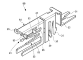
図13は側壁43を切り起こした変形例に係るバスバー13Bの斜視図、図14(a)は図13に示したバスバー13Bを2本並べた斜視図、(b)はその平面図である。
この変形例に係る電子部品11の接続構造は、図13に示すように、バスバー13Bの側壁43の先端部分と、それよりも後方部分とを切り起こし加工することにより、前後に一対の垂直片85を突出させている。バスバー13Bは、上記同様に、一対の接触バネ片23,24が平行となるように2本が並設されることで、この前側の垂直片85同士と、後側の垂直片85同士とが突き合わされる。この垂直片85同士の対向面は、反射面83となっている。
Next, another modification will be described.
13 is a perspective view of a
As shown in FIG. 13, the connection structure of the
これにより、発光部79は、図14に示すように、一対の平行な側壁43に形成した反射面83と、この反射面83に直交するそれぞれ2つの垂直片85を対向配置して連続させた一対の反射面83とによって4方が包囲され、漏れ光の発生を殆ど無くして、出射光がより有効に利用できるようになされている。
Thereby, as shown in FIG. 14, the
したがって、本実施の形態による電子部品11の接続構造によれば、バスバー13を一種類にして、接点間ピッチや外形状、大きさが異なる2種類の表面実装用の電子部品11を接続することができる。
Therefore, according to the connection structure of the
なお、上記第1実施の形態に係る電子部品11の接続構造では、2本の同一形状のバスバー13を構成の主要部として有している電子部品11の接続構造を説明したが、本発明に係る電子部品の接続構造はこれに限定されるものではなく、3本以上の同一形状のバスバーを構成の主要部としたものでもよい。
In the connection structure of the
図15〜図19に、本発明の第2実施形態に係る電子部品11Aの接続構造を用いた2灯のLEDユニット99を説明する。なお、上記第1実施形態に係る電子部品11の接続構造を用いたLEDユニット53と略同様の構成部材については、同符号を付して詳細な説明を省略する。
15 to 19, a two-
本第2実施形態に係る電子部品11Aの接続構造は、図15に示す3本の同一形状のバスバー13Cを構成の主要部として有している。この3本のバスバー13Cは、ハウジング91に収容されて使用される。
3本のバスバー13Cは、一端17にそれぞれ端子部19を形成し、離間して3列に並列配置される。端子部19は、複数種(本実施形態では2種類で3つ)の電子部品11Aの各一対の接点部21に弾接可能な少なくとも二対の平行な左右接触バネ片23a,24a、23b,24bが上下多段(本実施形態では2段)に配置して形成される。
The connection structure of the electronic component 11A according to the second embodiment has three
The three
1本のバスバー13Cには、略Y字状に分岐した一対の接触バネ片23,24の先端に二対の左右接触バネ片23a,24a、23b,24bが設けられる。3列に並列配置されたバスバー13Cの上段における6つの左右接触バネ片23a,24a,23a,24a,23a,24aのうち隣接する4つの左右接触バネ片24a,23a,24a,23aの電気接触部45が、3本のバスバー13C間に配置された第1の電子部品11Aである2個の半導体発光素子25の各一対の接点部21とそれぞれ接続する。また、3列に並列配置されたバスバー13Cの下段における6つの左右接触バネ片23b,24b,23b,24b,23b,24bのうち中央の2つの左右接触バネ片24b,23bを跨いだ2つの左右接触バネ片23b,24bの電気接触部45が3本のバスバー13C間で2個の半導体発光素子25の下方に位置する第2の電子部品11Aであるツエナーダイオード27の一対の接点部21と接続する。なお、本第2実施の形態におけるツエナーダイオード27は、接点間ピッチが、電気接触部45の接点間ピッチの3倍の距離となるものが用いられている。
One
すなわち、図15において、一方の半導体発光素子25は、3列に並列配置されたバスバー13Cの上段の電気接触部45において、左側から2番目の電気接触部45と、左側から3番目の電気接触部45とに接続され、他方の半導体発光素子25は、左側から4番目の電気接触部45と、左側から5番目の電気接触部45とに接続される。また、ツエナーダイオード27は、3列に並列配置されたバスバー13Cの下段の電気接触部45において、左側から2番目の電気接触部45と、左側から5番目の電気接触部45とに接続される。
That is, in FIG. 15, one of the semiconductor
次に、上記構成の電子部品11Aの接続構造の組付け工程を説明する。
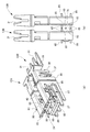
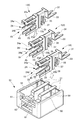
図15は本発明の第2実施形態に係る電子部品11Aの接続構造におけるバスバー組付け工程を説明する図、図16は同様に電子部品組付け工程を説明する図、図17は同様にハウジング組付け工程を説明する図、図18は同様に電線ホルダー組付け工程を説明する図、図19は本発明の第2実施形態に係る電子部品11Aの接続構造を用いたLEDユニット99の斜視図である。
上記の電子部品11Aの接続構造は、例えば2灯のLEDユニット99に好適に採用することができる。電子部品11Aの接続構造を2灯のLEDユニット99に適用するには、図15に示すように、3本のバスバー13Cをハウジング91に装着する。
Next, the assembly process of the connection structure of the electronic component 11A having the above configuration will be described.
15 is a diagram for explaining a bus bar assembling process in the connection structure of the electronic component 11A according to the second embodiment of the present invention, FIG. 16 is a diagram for similarly explaining the electronic component assembling process, and FIG. 18 is a diagram for explaining the attaching process, FIG. 18 is a diagram for explaining the electric wire holder assembling process, and FIG. 19 is a perspective view of the
The connection structure of the
ハウジング91には3つのバスバー収用室55が形成される。バスバー収用室55は、後端が後壁57となり、その前方の内壁面に一対の保持溝59がそれぞれのバスバー収用室55に形成されている。バスバー収用室55に挿入されたバスバー13Cは、後部当接片33と後部弾性脚35とで後壁57を挟持し、ハウジング91から脱落規制されて装着される。
In the
図16に示すように、ハウジング91の前面には左右2つのLED装着開口部61と、ダイオード装着開口部63とが上下2段で形成されている。各LED装着開口部61には、半導体発光素子25が、接点部21を下側にして挿入される。ダイオード装着開口部63には、ツエナーダイオード27が、接点部21を上側にして挿入される。これにより、それぞれの接点部21が、それぞれの対応する電気接触部45に接続される。また、ハウジング91の底面には抵抗装着開口部(図示せず)が形成されており、抵抗器28が挿入される。これにより、手前のバスバー13Cにおける前部当接片39と前部弾性脚37とで抵抗器28を挟持し、前部弾性脚37の電気接触部が抵抗器28の一対の接点部に接続される。
As shown in FIG. 16, two left and right
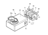
図17に示すように、2個の半導体発光素子25と、ツエナーダイオード27とを装着したハウジング91は、2つのレンズ95aを備えたレンズカバー95に装着される。レンズカバー95の後端面にはハウジング挿入開口97が形成されている。レンズカバー95に挿入されたハウジング91は、圧接刃31がレンズカバー95の内部で後方に向かって突出している。
As shown in FIG. 17, a
図18に示すように、ハウジング91を装着したレンズカバー95には電線ホルダー93がハウジング挿入開口97から挿入される。電線ホルダー93の3方の外面にはコ字状の電線保持溝71が3箇所に形成されている。両側の電線保持溝71には被覆付き電線29がコ字状に曲げられて装着される。電線ホルダー93の前面にはそれぞれの電線保持溝71を跨って、水平な圧接刃進入スリット73が形成されている。これにより、電線ホルダー93がレンズカバー95に挿入されると、レンズカバー95の内部で後方に向かって突出したバスバー13の圧接刃31が、圧接刃進入スリット73に進入し、圧接刃31と電線29の導体とが接続されるようになされている。
As shown in FIG. 18, the
レンズカバー95に挿入された電線ホルダー93は、レンズカバー95の側部に形成さける係止穴75に、側面に突設した係止爪77を係止して、レンズカバー95からのハウジング91と、電線ホルダー93自身との離脱が規制される。レンズカバー95に、ハウジング91、電線ホルダー93が装着されることで図19に示す2灯のLEDユニット99が構成される。
The
このように、本第2実施形態の電子部品11Aの接続構造は、二対の平行な左右接触バネ片23a,24a、23b,24bが上下2段に配置して形成された端子部19を有する3本のバスバー13Cが離間して3列に並列配置される。そして、3列に並列配置されたバスバー13Cの上段における6つの左右接触バネ片23a,24a,23a,24a,23a,24aのうち隣接する4つの左右接触バネ片24a,23a,24a,23aの電気接触部45が、3本のバスバー13C間に配置された2個の半導体発光素子25の各一対の接点部21に接続される。また、3列に並列配置されたバスバー13Cの下段における6つの左右接触バネ片23b,24b,23b,24b,23b,24bのうち中央の2つの左右接触バネ片24b,23bを跨いだ2つの左右接触バネ片23b,24bの電気接触部45が3本のバスバー13C間で2個の半導体発光素子25の下方に位置するツエナーダイオード27の一対の接点部21に接続され、外形状や大きさ、接点間ピッチが異なる電子部品11Aが接続可能となる。
As described above, the connection structure of the electronic component 11A of the second embodiment includes the
なお、本第2実施形態に係る2灯のLEDユニット99は、ツエナーダイオード27を装着しなくとも、2個の半導体発光素子25を発光させることは可能であり、ツエナーダイオード27を省略して部品点数を減らすこともできる。
上述した様に、本発明の電子部品の接続構造によれば、一種類のバスバーを用いて、接点間のピッチや外形状、大きさ等が異なる複数種の表面実装用の電子部品を種々の接続回路形態に接続することができる。
The two-
As described above, according to the electronic component connection structure of the present invention, various types of electronic components for surface mounting having different pitches, outer shapes, sizes, and the like between the contacts are used by using one type of bus bar. Connection circuit form can be connected.
11 電子部品
13 バスバー
17 一端
19 端子部
21 接点部
23 接触バネ片
23a,24a 左右接触バネ片
23b,24b 左右接触バネ片
24 接触バネ片
25 半導体発光素子(第1の電子部品)
27 ツエナーダイオード(第2の電子部品)
43 側壁
45 電気接触部
79 発光部
81 側壁面
83 反射面
DESCRIPTION OF
27 Zener diode (second electronic component)
43
Claims (4)
並列配置された前記バスバーの各段における前記左右接触バネ片のうち少なくとも何れか2片が前記バスバー間に配置された複数種の前記電子部品の各一対の前記接点部と接続されることを特徴とする電子部品の接続構造。 A plurality of bus bars each having a terminal portion formed at one end thereof are arranged in parallel at a distance from each other, and each terminal portion has at least two pairs of parallel left and right contact spring pieces capable of elastically contacting each pair of contact portions of a plurality of electronic components. Are arranged in multiple stages,
At least any two of the left and right contact spring pieces in each stage of the bus bars arranged in parallel are connected to a pair of contact portions of a plurality of types of the electronic components arranged between the bus bars. Connection structure for electronic components.
前記バスバーは、略Y字状に分岐した一対の接触バネ片の先端に二対の前記左右接触バネ片を有し、
2本の前記バスバーを平行に離間配置することで前記左右接触バネ片の先端部の電気接触部が片側4箇所ずつの8箇所に配置され、
一方の段では隣接する前記左右接触バネ片の電気接触部に第1の前記電子部品の一対の接点部が接触し、他方の段では少なくとも1つの電気接触部を跨いで前記左右接触バネ片の電気接触部に第2の前記電子部品の一対の接点部が接触することを特徴とする電子部品の接続構造。 The electronic component connection structure according to claim 1,
The bus bar has two pairs of left and right contact spring pieces at the ends of a pair of contact spring pieces branched in a substantially Y shape,
By arranging the two bus bars apart from each other in parallel, the electrical contact portions of the tip portions of the left and right contact spring pieces are arranged at eight locations on four sides,
In one stage, the pair of contact parts of the first electronic component is in contact with the electrical contact portions of the adjacent left and right contact spring pieces, and in the other stage, the left and right contact spring pieces straddle at least one electrical contact part. A connection structure for an electronic component, wherein the pair of contact portions of the second electronic component are in contact with the electrical contact portion.
前記バスバーは、一対の側壁が平行となるようにU字状に折り曲げ形成され、
前記側壁のそれぞれに前記接触バネ片が打ち抜き成形されていることを特徴とする電子部品の接続構造。 The electronic component connection structure according to claim 2,
The bus bar is formed to be bent in a U shape so that a pair of side walls are parallel,
The connection structure for an electronic component, wherein the contact spring piece is stamped and formed on each of the side walls.
前記電子部品の1つが半導体発光素子であり、
前記半導体発光素子は、発光部が2本の前記バスバーの間に配置され、
前記バスバーの前記発光部を挟むそれぞれの側壁面には反射面が形成されることを特徴とする電子部品の接続構造。 It is the connection structure of the electronic component of any one of Claims 1-3,
One of the electronic components is a semiconductor light emitting device,
The semiconductor light emitting device has a light emitting portion disposed between the two bus bars,
A connection structure for an electronic component, wherein a reflection surface is formed on each side wall surface of the bus bar sandwiching the light emitting portion.
Priority Applications (6)
| Application Number | Priority Date | Filing Date | Title |
|---|---|---|---|
| JP2011180846A JP2012124149A (en) | 2010-11-18 | 2011-08-22 | Structure for connecting electronic component |
| CN2011800557397A CN103222122A (en) | 2010-11-18 | 2011-11-18 | Connection Structure of Electronic Devices |
| DE112011103841T DE112011103841T5 (en) | 2010-11-18 | 2011-11-18 | Connection setup for electronic components |
| KR1020137012566A KR20130067316A (en) | 2010-11-18 | 2011-11-18 | Connecting structure for electronic devices |
| PCT/JP2011/077278 WO2012067271A1 (en) | 2010-11-18 | 2011-11-18 | Connecting Structure for Electronic Devices |
| US13/895,006 US20130252483A1 (en) | 2010-11-18 | 2013-05-15 | Connecting structure for electronic devices |
Applications Claiming Priority (3)
| Application Number | Priority Date | Filing Date | Title |
|---|---|---|---|
| JP2010258229 | 2010-11-18 | ||
| JP2010258229 | 2010-11-18 | ||
| JP2011180846A JP2012124149A (en) | 2010-11-18 | 2011-08-22 | Structure for connecting electronic component |
Publications (1)
| Publication Number | Publication Date |
|---|---|
| JP2012124149A true JP2012124149A (en) | 2012-06-28 |
Family
ID=45218824
Family Applications (1)
| Application Number | Title | Priority Date | Filing Date |
|---|---|---|---|
| JP2011180846A Withdrawn JP2012124149A (en) | 2010-11-18 | 2011-08-22 | Structure for connecting electronic component |
Country Status (6)
| Country | Link |
|---|---|
| US (1) | US20130252483A1 (en) |
| JP (1) | JP2012124149A (en) |
| KR (1) | KR20130067316A (en) |
| CN (1) | CN103222122A (en) |
| DE (1) | DE112011103841T5 (en) |
| WO (1) | WO2012067271A1 (en) |
Cited By (3)
| Publication number | Priority date | Publication date | Assignee | Title |
|---|---|---|---|---|
| WO2014119356A1 (en) * | 2013-01-29 | 2014-08-07 | 矢崎総業株式会社 | Connection structure for electric components |
| WO2014126168A1 (en) * | 2013-02-14 | 2014-08-21 | 矢崎総業株式会社 | Semiconductor light source unit and vehicle lighting device |
| WO2017150567A1 (en) * | 2016-03-01 | 2017-09-08 | 矢崎総業株式会社 | Terminal housing and wire harness |
Families Citing this family (8)
| Publication number | Priority date | Publication date | Assignee | Title |
|---|---|---|---|---|
| JP5669304B2 (en) * | 2010-11-19 | 2015-02-12 | 矢崎総業株式会社 | Electronic component connection structure |
| JP2013182878A (en) * | 2012-03-05 | 2013-09-12 | Yazaki Corp | Connection structure for electronic component |
| CN115313081A (en) | 2017-04-24 | 2022-11-08 | 康普技术有限责任公司 | Connector for single twisted conductor pairs |
| CN111937243B (en) * | 2018-02-26 | 2022-07-15 | 康普技术有限责任公司 | Connector and contact for single twisted conductor pairs |
| USD924810S1 (en) | 2019-01-04 | 2021-07-13 | Intel Corporation | Busbar |
| EP4038430A4 (en) | 2019-09-30 | 2024-02-28 | CommScope Technologies LLC | HIGH DENSITY CLUTCH PLATE |
| US12316055B2 (en) | 2019-09-30 | 2025-05-27 | Commscope Technologies Llc | Couplers for single pair connectors |
| US12199372B2 (en) | 2021-02-26 | 2025-01-14 | Commscope Technologies Llc | Couplers for single pair connectors |
Family Cites Families (14)
| Publication number | Priority date | Publication date | Assignee | Title |
|---|---|---|---|---|
| US5618187A (en) * | 1994-11-17 | 1997-04-08 | The Whitaker Corporation | Board mount bus bar contact |
| US6319075B1 (en) * | 1998-04-17 | 2001-11-20 | Fci Americas Technology, Inc. | Power connector |
| US6776635B2 (en) * | 2001-06-14 | 2004-08-17 | Tyco Electronics Corporation | Multi-beam power contact for an electrical connector |
| JP2005085861A (en) * | 2003-09-05 | 2005-03-31 | Yazaki Corp | LED lamp |
| US7210957B2 (en) * | 2004-04-06 | 2007-05-01 | Lumination Llc | Flexible high-power LED lighting system |
| DE102004061681B4 (en) * | 2004-12-22 | 2006-10-26 | Adc Gmbh | Cable connectors for printed circuit boards |
| US7156689B2 (en) * | 2005-01-14 | 2007-01-02 | Tyco Electronics Corporation | Dual wire connector with multiple press fit connection |
| JP4754333B2 (en) | 2005-11-24 | 2011-08-24 | 矢崎総業株式会社 | Electronic component connection structure |
| CN101740976B (en) * | 2008-11-05 | 2012-04-11 | 泰科电子(上海)有限公司 | LED (Light Emitting Diode) socket and LED module |
| JP5557368B2 (en) | 2009-04-24 | 2014-07-23 | 学校法人東京電機大学 | Semiconductor inspection apparatus and semiconductor inspection method |
| CN201611080U (en) * | 2009-10-10 | 2010-10-20 | 秀山交通器材股份有限公司 | Adapter for vehicle lamp |
| JP2011180846A (en) | 2010-03-01 | 2011-09-15 | Art Technology Co Ltd | Noncontact communication system and induction coil device for use therein |
| JP2012109162A (en) * | 2010-11-18 | 2012-06-07 | Yazaki Corp | Connection structure of electronic component |
| JP5718631B2 (en) * | 2010-12-22 | 2015-05-13 | 矢崎総業株式会社 | Electronic component connection structure |
-
2011
- 2011-08-22 JP JP2011180846A patent/JP2012124149A/en not_active Withdrawn
- 2011-11-18 CN CN2011800557397A patent/CN103222122A/en active Pending
- 2011-11-18 WO PCT/JP2011/077278 patent/WO2012067271A1/en not_active Ceased
- 2011-11-18 DE DE112011103841T patent/DE112011103841T5/en not_active Withdrawn
- 2011-11-18 KR KR1020137012566A patent/KR20130067316A/en not_active Ceased
-
2013
- 2013-05-15 US US13/895,006 patent/US20130252483A1/en not_active Abandoned
Cited By (7)
| Publication number | Priority date | Publication date | Assignee | Title |
|---|---|---|---|---|
| WO2014119356A1 (en) * | 2013-01-29 | 2014-08-07 | 矢崎総業株式会社 | Connection structure for electric components |
| JP2014146484A (en) * | 2013-01-29 | 2014-08-14 | Yazaki Corp | Connection structure of electric component |
| CN104956552A (en) * | 2013-01-29 | 2015-09-30 | 矢崎总业株式会社 | Connection structure for electric components |
| WO2014126168A1 (en) * | 2013-02-14 | 2014-08-21 | 矢崎総業株式会社 | Semiconductor light source unit and vehicle lighting device |
| JP2014157689A (en) * | 2013-02-14 | 2014-08-28 | Yazaki Corp | Semiconductor light source unit and vehicle lighting device |
| WO2017150567A1 (en) * | 2016-03-01 | 2017-09-08 | 矢崎総業株式会社 | Terminal housing and wire harness |
| US10686309B2 (en) | 2016-03-01 | 2020-06-16 | Yazaki Corporation | Terminal accommodating body and wire harness |
Also Published As
| Publication number | Publication date |
|---|---|
| CN103222122A (en) | 2013-07-24 |
| WO2012067271A1 (en) | 2012-05-24 |
| US20130252483A1 (en) | 2013-09-26 |
| DE112011103841T5 (en) | 2013-08-29 |
| KR20130067316A (en) | 2013-06-21 |
Similar Documents
| Publication | Publication Date | Title |
|---|---|---|
| JP5669304B2 (en) | Electronic component connection structure | |
| US20130252483A1 (en) | Connecting structure for electronic devices | |
| JP5718631B2 (en) | Electronic component connection structure | |
| JP2012134055A (en) | Electronic component connecting structure, and electronic component connecting unit | |
| JP2013171800A (en) | Structure of lighting unit | |
| JP2012109162A (en) | Connection structure of electronic component | |
| JP2013182879A (en) | Electronic component connection structure | |
| JP4345016B2 (en) | Light emitting device | |
| JP2013243053A (en) | Connection structure for electronic component | |
| US9209579B2 (en) | Connecting structure for electronic device | |
| JP2009146579A (en) | Connector | |
| US20140363993A1 (en) | Connection structure of electronic components | |
| JP2013080678A (en) | Connection structure of electronic component | |
| JP2013218797A (en) | Connection structure of electronic component | |
| JP2014157689A (en) | Semiconductor light source unit and vehicle lighting device | |
| JP2013229256A (en) | Light-emitting unit | |
| JP4587922B2 (en) | Terminal blocks and lighting fixtures | |
| JP2008071646A (en) | Connection member | |
| JP2014146484A (en) | Connection structure of electric component | |
| JP2013182877A (en) | Structure of lighting unit |
Legal Events
| Date | Code | Title | Description |
|---|---|---|---|
| A300 | Application deemed to be withdrawn because no request for examination was validly filed |
Free format text: JAPANESE INTERMEDIATE CODE: A300 Effective date: 20141104 |