JP2012124306A - 半導体発光素子 - Google Patents
半導体発光素子 Download PDFInfo
- Publication number
- JP2012124306A JP2012124306A JP2010273485A JP2010273485A JP2012124306A JP 2012124306 A JP2012124306 A JP 2012124306A JP 2010273485 A JP2010273485 A JP 2010273485A JP 2010273485 A JP2010273485 A JP 2010273485A JP 2012124306 A JP2012124306 A JP 2012124306A
- Authority
- JP
- Japan
- Prior art keywords
- layer
- light emitting
- transparent electrode
- reflective layer
- emitting device
- Prior art date
- Legal status (The legal status is an assumption and is not a legal conclusion. Google has not performed a legal analysis and makes no representation as to the accuracy of the status listed.)
- Pending
Links
Images


Classifications
-
- H—ELECTRICITY
- H10—SEMICONDUCTOR DEVICES; ELECTRIC SOLID-STATE DEVICES NOT OTHERWISE PROVIDED FOR
- H10H—INORGANIC LIGHT-EMITTING SEMICONDUCTOR DEVICES HAVING POTENTIAL BARRIERS
- H10H20/00—Individual inorganic light-emitting semiconductor devices having potential barriers, e.g. light-emitting diodes [LED]
- H10H20/80—Constructional details
- H10H20/83—Electrodes
- H10H20/832—Electrodes characterised by their material
- H10H20/833—Transparent materials
-
- H—ELECTRICITY
- H10—SEMICONDUCTOR DEVICES; ELECTRIC SOLID-STATE DEVICES NOT OTHERWISE PROVIDED FOR
- H10H—INORGANIC LIGHT-EMITTING SEMICONDUCTOR DEVICES HAVING POTENTIAL BARRIERS
- H10H20/00—Individual inorganic light-emitting semiconductor devices having potential barriers, e.g. light-emitting diodes [LED]
- H10H20/80—Constructional details
- H10H20/83—Electrodes
- H10H20/831—Electrodes characterised by their shape
-
- H—ELECTRICITY
- H10—SEMICONDUCTOR DEVICES; ELECTRIC SOLID-STATE DEVICES NOT OTHERWISE PROVIDED FOR
- H10H—INORGANIC LIGHT-EMITTING SEMICONDUCTOR DEVICES HAVING POTENTIAL BARRIERS
- H10H20/00—Individual inorganic light-emitting semiconductor devices having potential barriers, e.g. light-emitting diodes [LED]
- H10H20/80—Constructional details
- H10H20/84—Coatings, e.g. passivation layers or antireflective coatings
- H10H20/841—Reflective coatings, e.g. dielectric Bragg reflectors
-
- H—ELECTRICITY
- H10—SEMICONDUCTOR DEVICES; ELECTRIC SOLID-STATE DEVICES NOT OTHERWISE PROVIDED FOR
- H10H—INORGANIC LIGHT-EMITTING SEMICONDUCTOR DEVICES HAVING POTENTIAL BARRIERS
- H10H20/00—Individual inorganic light-emitting semiconductor devices having potential barriers, e.g. light-emitting diodes [LED]
- H10H20/80—Constructional details
- H10H20/81—Bodies
- H10H20/822—Materials of the light-emitting regions
- H10H20/824—Materials of the light-emitting regions comprising only Group III-V materials, e.g. GaP
- H10H20/825—Materials of the light-emitting regions comprising only Group III-V materials, e.g. GaP containing nitrogen, e.g. GaN
Landscapes
- Led Devices (AREA)
Abstract
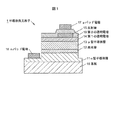
【解決手段】本発明の一態様に係る半導体発光素子1は、n型半導体層11とp型半導体層13とに挟まれた発光層12を有する半導体積層構造を有する半導体発光素子であって、p型半導体層13上に形成された第1の透明電極14と、第1の透明電極14上に形成された、第1の透明電極14よりも面積の小さい反射層15と、第1の透明電極14上に反射層15を覆うように形成された第2の透明電極16と、第2の透明電極16上の反射層15の上方の領域に形成されたpパッド電極17と、を有する。
【選択図】図1
Description
11 n型半導体層
12 発光層
13 p型半導体層
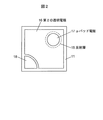
14 第1の透明電極
15 反射層
16 第2の透明電極
17 pパッド電極
Claims (3)
- 第1導電型層と第2導電型層とに挟まれた発光層を有する半導体積層構造を有する半導体発光素子であって、
前記第2導電型層上に形成された第1の透明電極と、
前記第1の透明電極上に形成された、前記第1の透明電極よりも面積の小さい反射層と、
前記第1の透明電極上に前記反射層を覆うように形成された第2の透明電極と、
前記第2の透明電極上の前記反射層の上方の領域に形成されたパッド電極と、
を有する半導体発光素子。 - 前記反射層は、透明絶縁体に表面を覆われた金属からなる、
請求項1に記載の半導体発光素子。 - 前記第1の透明電極と前記第2の透明電極の接触領域は、前記反射層の底面の周囲を囲む、
請求項1または2に記載の半導体発光素子。
Priority Applications (3)
| Application Number | Priority Date | Filing Date | Title |
|---|---|---|---|
| JP2010273485A JP2012124306A (ja) | 2010-12-08 | 2010-12-08 | 半導体発光素子 |
| US13/317,692 US9117973B2 (en) | 2010-12-08 | 2011-10-26 | Semiconductor light emitting element |
| CN201110402374.2A CN102569589B (zh) | 2010-12-08 | 2011-12-06 | 半导体发光元件 |
Applications Claiming Priority (1)
| Application Number | Priority Date | Filing Date | Title |
|---|---|---|---|
| JP2010273485A JP2012124306A (ja) | 2010-12-08 | 2010-12-08 | 半導体発光素子 |
Publications (1)
| Publication Number | Publication Date |
|---|---|
| JP2012124306A true JP2012124306A (ja) | 2012-06-28 |
Family
ID=46198457
Family Applications (1)
| Application Number | Title | Priority Date | Filing Date |
|---|---|---|---|
| JP2010273485A Pending JP2012124306A (ja) | 2010-12-08 | 2010-12-08 | 半導体発光素子 |
Country Status (3)
| Country | Link |
|---|---|
| US (1) | US9117973B2 (ja) |
| JP (1) | JP2012124306A (ja) |
| CN (1) | CN102569589B (ja) |
Cited By (7)
| Publication number | Priority date | Publication date | Assignee | Title |
|---|---|---|---|---|
| WO2014092448A1 (ko) * | 2012-12-14 | 2014-06-19 | 서울바이오시스 주식회사 | 광추출 효율이 향상된 발광다이오드 |
| US20150179890A1 (en) * | 2013-12-19 | 2015-06-25 | Nichia Corporation | Semiconductor light emitting element |
| JP2017117904A (ja) * | 2015-12-24 | 2017-06-29 | 日亜化学工業株式会社 | 発光素子及びその製造方法 |
| KR20170074239A (ko) * | 2014-10-29 | 2017-06-29 | 오스람 옵토 세미컨덕터스 게엠베하 | 광전자 반도체 칩 |
| JP2017152547A (ja) * | 2016-02-25 | 2017-08-31 | 日亜化学工業株式会社 | 発光素子 |
| JP2018006535A (ja) * | 2016-06-30 | 2018-01-11 | ウシオ電機株式会社 | 半導体発光素子 |
| US12224389B2 (en) | 2020-09-07 | 2025-02-11 | Nichia Corporation | Light-emitting element including a reflective portion having a first, second, and third layer |
Families Citing this family (9)
| Publication number | Priority date | Publication date | Assignee | Title |
|---|---|---|---|---|
| CN104205369A (zh) * | 2012-03-19 | 2014-12-10 | 皇家飞利浦有限公司 | 在硅衬底上生长的发光器件 |
| CN103022306B (zh) * | 2012-12-21 | 2015-05-06 | 安徽三安光电有限公司 | 发光二极管及其制作方法 |
| KR102085897B1 (ko) * | 2013-06-10 | 2020-03-06 | 엘지이노텍 주식회사 | 발광 소자 및 발광 소자 패키지 |
| TWI536602B (zh) * | 2013-10-25 | 2016-06-01 | 隆達電子股份有限公司 | 發光二極體 |
| CN104638084B (zh) * | 2013-11-11 | 2019-07-02 | 晶元光电股份有限公司 | 发光元件 |
| DE102013113106A1 (de) * | 2013-11-27 | 2015-06-11 | Osram Opto Semiconductors Gmbh | Strahlung emittierender Halbleiterchip |
| DE102016101612A1 (de) * | 2016-01-29 | 2017-08-03 | Osram Opto Semiconductors Gmbh | Optoelektronischer Halbleiterchip und Verfahren zur Herstellung eines optoelektronischen Halbleiterchips |
| KR102302592B1 (ko) | 2017-07-18 | 2021-09-15 | 삼성전자주식회사 | 반도체 발광 소자 |
| CN118367072A (zh) * | 2024-04-16 | 2024-07-19 | 泉州三安半导体科技有限公司 | 发光二极管及发光装置 |
Citations (7)
| Publication number | Priority date | Publication date | Assignee | Title |
|---|---|---|---|---|
| JP2004200303A (ja) * | 2002-12-17 | 2004-07-15 | Sharp Corp | 発光ダイオード |
| US20050087884A1 (en) * | 2003-10-24 | 2005-04-28 | Stokes Edward B. | Flip-chip light emitting diode |
| JP2006108161A (ja) * | 2004-09-30 | 2006-04-20 | Toyoda Gosei Co Ltd | 半導体発光素子 |
| JP2008192690A (ja) * | 2007-02-01 | 2008-08-21 | Nichia Chem Ind Ltd | 半導体発光素子 |
| US20080303034A1 (en) * | 2007-06-08 | 2008-12-11 | Kuo-Chin Huang | Light-emitting gallium nitride-based III-V group compound semiconductor device and manufacturing method thereof |
| JP2008300719A (ja) * | 2007-06-01 | 2008-12-11 | Nichia Corp | 半導体発光素子およびその製造方法 |
| JP2009010280A (ja) * | 2007-06-29 | 2009-01-15 | Nichia Corp | 半導体発光素子 |
Family Cites Families (12)
| Publication number | Priority date | Publication date | Assignee | Title |
|---|---|---|---|---|
| JPH11220212A (ja) * | 1998-02-02 | 1999-08-10 | Toshiba Corp | 光素子、光素子の駆動方法及び半導体レーザ素子 |
| JP4024463B2 (ja) * | 1999-09-27 | 2007-12-19 | シャープ株式会社 | 半導体発光素子の製造方法 |
| JP3975388B2 (ja) | 2000-04-07 | 2007-09-12 | サンケン電気株式会社 | 半導体発光素子 |
| JP4054631B2 (ja) * | 2001-09-13 | 2008-02-27 | シャープ株式会社 | 半導体発光素子およびその製造方法、ledランプ並びにled表示装置 |
| JP2004128452A (ja) * | 2002-07-31 | 2004-04-22 | Shin Etsu Handotai Co Ltd | 発光素子の製造方法及び発光素子 |
| US7109048B2 (en) * | 2003-09-30 | 2006-09-19 | Lg Electronics Inc. | Semiconductor light emitting device and fabrication method thereof |
| US7417264B2 (en) * | 2003-12-22 | 2008-08-26 | Samsung Electronics Co., Ltd. | Top-emitting nitride-based light emitting device and method of manufacturing the same |
| KR100580634B1 (ko) * | 2003-12-24 | 2006-05-16 | 삼성전자주식회사 | 질화물계 발광소자 및 그 제조방법 |
| US7291865B2 (en) | 2004-09-29 | 2007-11-06 | Toyoda Gosei Co., Ltd. | Light-emitting semiconductor device |
| US8026527B2 (en) * | 2007-12-06 | 2011-09-27 | Bridgelux, Inc. | LED structure |
| KR101134720B1 (ko) * | 2009-02-16 | 2012-04-13 | 엘지이노텍 주식회사 | 반도체 발광소자 및 그 제조방법 |
| JP5332882B2 (ja) * | 2009-04-30 | 2013-11-06 | 豊田合成株式会社 | 半導体発光素子 |
-
2010
- 2010-12-08 JP JP2010273485A patent/JP2012124306A/ja active Pending
-
2011
- 2011-10-26 US US13/317,692 patent/US9117973B2/en active Active
- 2011-12-06 CN CN201110402374.2A patent/CN102569589B/zh active Active
Patent Citations (7)
| Publication number | Priority date | Publication date | Assignee | Title |
|---|---|---|---|---|
| JP2004200303A (ja) * | 2002-12-17 | 2004-07-15 | Sharp Corp | 発光ダイオード |
| US20050087884A1 (en) * | 2003-10-24 | 2005-04-28 | Stokes Edward B. | Flip-chip light emitting diode |
| JP2006108161A (ja) * | 2004-09-30 | 2006-04-20 | Toyoda Gosei Co Ltd | 半導体発光素子 |
| JP2008192690A (ja) * | 2007-02-01 | 2008-08-21 | Nichia Chem Ind Ltd | 半導体発光素子 |
| JP2008300719A (ja) * | 2007-06-01 | 2008-12-11 | Nichia Corp | 半導体発光素子およびその製造方法 |
| US20080303034A1 (en) * | 2007-06-08 | 2008-12-11 | Kuo-Chin Huang | Light-emitting gallium nitride-based III-V group compound semiconductor device and manufacturing method thereof |
| JP2009010280A (ja) * | 2007-06-29 | 2009-01-15 | Nichia Corp | 半導体発光素子 |
Cited By (20)
| Publication number | Priority date | Publication date | Assignee | Title |
|---|---|---|---|---|
| WO2014092448A1 (ko) * | 2012-12-14 | 2014-06-19 | 서울바이오시스 주식회사 | 광추출 효율이 향상된 발광다이오드 |
| US10243109B2 (en) | 2012-12-14 | 2019-03-26 | Seoul Viosys Co., Ltd. | Light-emitting diode with improved light extraction efficiency |
| US9978910B2 (en) | 2012-12-14 | 2018-05-22 | Seoul Viosys Co., Ltd. | Light-emitting diode with improved light extraction efficiency |
| US9401456B2 (en) | 2012-12-14 | 2016-07-26 | Seoul Viosys Co., Ltd. | Light-emitting diode with improved light extraction efficiency |
| US9293658B2 (en) | 2013-12-19 | 2016-03-22 | Nichia Corporation | Semiconductor light emitting element |
| JP2015135951A (ja) * | 2013-12-19 | 2015-07-27 | 日亜化学工業株式会社 | 半導体発光素子 |
| US9123865B2 (en) | 2013-12-19 | 2015-09-01 | Nichia Corporation | Semiconductor light emitting element |
| US20150179890A1 (en) * | 2013-12-19 | 2015-06-25 | Nichia Corporation | Semiconductor light emitting element |
| US20150325751A1 (en) * | 2013-12-19 | 2015-11-12 | Nichia Corporation | Semiconductor light emitting element |
| TWI649898B (zh) * | 2013-12-19 | 2019-02-01 | 日商日亞化學工業股份有限公司 | 半導體發光元件及其製造方法 |
| KR20170074239A (ko) * | 2014-10-29 | 2017-06-29 | 오스람 옵토 세미컨덕터스 게엠베하 | 광전자 반도체 칩 |
| JP2017533591A (ja) * | 2014-10-29 | 2017-11-09 | オスラム オプト セミコンダクターズ ゲゼルシャフト ミット ベシュレンクテル ハフツングOsram Opto Semiconductors GmbH | 光電子半導体チップ |
| US10079329B2 (en) | 2014-10-29 | 2018-09-18 | Osram Opto Semiconductors Gmbh | Optoelectronic semiconductor chip |
| KR102455387B1 (ko) * | 2014-10-29 | 2022-10-14 | 에이엠에스-오스람 인터내셔널 게엠베하 | 광전자 반도체 칩 |
| JP2017117904A (ja) * | 2015-12-24 | 2017-06-29 | 日亜化学工業株式会社 | 発光素子及びその製造方法 |
| JP2017152547A (ja) * | 2016-02-25 | 2017-08-31 | 日亜化学工業株式会社 | 発光素子 |
| JP2018006535A (ja) * | 2016-06-30 | 2018-01-11 | ウシオ電機株式会社 | 半導体発光素子 |
| JP2021129121A (ja) * | 2016-06-30 | 2021-09-02 | ウシオ電機株式会社 | 光照射装置 |
| JP7228120B2 (ja) | 2016-06-30 | 2023-02-24 | ウシオ電機株式会社 | 光照射装置 |
| US12224389B2 (en) | 2020-09-07 | 2025-02-11 | Nichia Corporation | Light-emitting element including a reflective portion having a first, second, and third layer |
Also Published As
| Publication number | Publication date |
|---|---|
| US9117973B2 (en) | 2015-08-25 |
| CN102569589A (zh) | 2012-07-11 |
| CN102569589B (zh) | 2014-12-10 |
| US20120146075A1 (en) | 2012-06-14 |
Similar Documents
| Publication | Publication Date | Title |
|---|---|---|
| US9117973B2 (en) | Semiconductor light emitting element | |
| JP5793292B2 (ja) | 半導体発光素子 | |
| CN102386294B (zh) | 发光元件 | |
| JP5494005B2 (ja) | 半導体発光素子 | |
| KR100876737B1 (ko) | 반도체 발광소자 및 그 제조방법 | |
| JP5589812B2 (ja) | 半導体発光素子 | |
| JP4889193B2 (ja) | 窒化物半導体発光素子 | |
| JP4450199B2 (ja) | 半導体発光素子 | |
| TWI602323B (zh) | 發光元件 | |
| JP6217528B2 (ja) | 発光素子 | |
| JP5605189B2 (ja) | 半導体発光素子 | |
| US20140138731A1 (en) | Semiconductor light emitting element | |
| JP4875361B2 (ja) | 3族窒化物発光素子 | |
| JP2012204373A (ja) | 半導体発光素子 | |
| TW201505211A (zh) | 發光元件 | |
| JP5543164B2 (ja) | 発光素子 | |
| JP5381822B2 (ja) | 半導体発光素子及びその製造方法 | |
| JP5991348B2 (ja) | 半導体発光素子 |
Legal Events
| Date | Code | Title | Description |
|---|---|---|---|
| A621 | Written request for application examination |
Free format text: JAPANESE INTERMEDIATE CODE: A621 Effective date: 20130125 |
|
| A977 | Report on retrieval |
Free format text: JAPANESE INTERMEDIATE CODE: A971007 Effective date: 20130828 |
|
| A131 | Notification of reasons for refusal |
Free format text: JAPANESE INTERMEDIATE CODE: A131 Effective date: 20131008 |
|
| A521 | Request for written amendment filed |
Free format text: JAPANESE INTERMEDIATE CODE: A523 Effective date: 20131206 |
|
| A131 | Notification of reasons for refusal |
Free format text: JAPANESE INTERMEDIATE CODE: A131 Effective date: 20140805 |
|
| A521 | Request for written amendment filed |
Free format text: JAPANESE INTERMEDIATE CODE: A523 Effective date: 20140922 |
|
| A02 | Decision of refusal |
Free format text: JAPANESE INTERMEDIATE CODE: A02 Effective date: 20150303 |