JP2012128559A - 演算処理装置 - Google Patents
演算処理装置 Download PDFInfo
- Publication number
- JP2012128559A JP2012128559A JP2010278041A JP2010278041A JP2012128559A JP 2012128559 A JP2012128559 A JP 2012128559A JP 2010278041 A JP2010278041 A JP 2010278041A JP 2010278041 A JP2010278041 A JP 2010278041A JP 2012128559 A JP2012128559 A JP 2012128559A
- Authority
- JP
- Japan
- Prior art keywords
- data
- arithmetic processing
- stride
- address
- instruction
- Prior art date
- Legal status (The legal status is an assumption and is not a legal conclusion. Google has not performed a legal analysis and makes no representation as to the accuracy of the status listed.)
- Granted
Links
Images






Classifications
-
- G—PHYSICS
- G06—COMPUTING OR CALCULATING; COUNTING
- G06F—ELECTRIC DIGITAL DATA PROCESSING
- G06F9/00—Arrangements for program control, e.g. control units
- G06F9/06—Arrangements for program control, e.g. control units using stored programs, i.e. using an internal store of processing equipment to receive or retain programs
- G06F9/30—Arrangements for executing machine instructions, e.g. instruction decode
- G06F9/30003—Arrangements for executing specific machine instructions
- G06F9/30007—Arrangements for executing specific machine instructions to perform operations on data operands
- G06F9/30036—Instructions to perform operations on packed data, e.g. vector, tile or matrix operations
-
- G—PHYSICS
- G06—COMPUTING OR CALCULATING; COUNTING
- G06F—ELECTRIC DIGITAL DATA PROCESSING
- G06F9/00—Arrangements for program control, e.g. control units
- G06F9/06—Arrangements for program control, e.g. control units using stored programs, i.e. using an internal store of processing equipment to receive or retain programs
- G06F9/30—Arrangements for executing machine instructions, e.g. instruction decode
- G06F9/34—Addressing or accessing the instruction operand or the result ; Formation of operand address; Addressing modes
- G06F9/345—Addressing or accessing the instruction operand or the result ; Formation of operand address; Addressing modes of multiple operands or results
- G06F9/3455—Addressing or accessing the instruction operand or the result ; Formation of operand address; Addressing modes of multiple operands or results using stride
Landscapes
- Engineering & Computer Science (AREA)
- Software Systems (AREA)
- Theoretical Computer Science (AREA)
- Physics & Mathematics (AREA)
- General Engineering & Computer Science (AREA)
- General Physics & Mathematics (AREA)
- Mathematical Physics (AREA)
- Advance Control (AREA)
- Executing Machine-Instructions (AREA)
- Complex Calculations (AREA)
Abstract
【解決手段】同時アクセス可能な複数のメモリブロックbank0〜bank3を有するデータメモリ2との間でデータを遣り取りする複数のベクトルパイプライン121〜124を有する演算処理装置であって、前記データメモリに対するストライドアクセスを、基本パターンのデータサイズを決める第1パラメータと、該基本パターンにおける有効なデータ数を決める第2パラメータで規定する。
【選択図】図3
Description
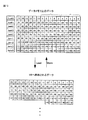
バンクメモリの物理アドレス
=(データのバイトアドレス)÷(各バンクのラインサイズ × バンク数)
=(データのバイトアドレス)÷(16 × 4)
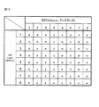
CNT×N≧DST
(付記1)
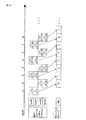
同時アクセス可能な複数のメモリブロックを有するデータメモリとの間でデータを遣り取りする複数のベクトルパイプラインを有する演算処理装置であって、
前記データメモリに対するストライドアクセスを、基本パターンのデータサイズを決める第1パラメータと、該基本パターンにおける有効なデータ数を決める第2パラメータで規定することを特徴とする演算処理装置。
前記第1パラメータをDSTとし、前記第2パラメータをCNTとし、前記同時アクセス可能なメモリブロックの数をNとするとき、DSTおよびCNTは、CNT×N≧DSTを満たす整数として規定されることを特徴とする付記1に記載の演算処理装置。
さらに、第1ビット幅を有する第1レジスタを有し、
前記ストライドアクセスにより同時にアクセスされるメモリブロックの数は、前記第1ビット幅に従って規定されることを特徴とする付記1または2に記載の演算処理装置。
前記第1レジスタは、前記第1ビット幅の複数のエントリを有するベクトルレジスタであることを特徴とする付記2または3に記載の演算処理装置。
前記ストライドアクセスは、ストライドロード/ストア命令によるアクセスであり、
デコードした命令が前記ストライドロード/ストア命令のとき、該ストライドロード/ストア命令の先行命令がロード/ストア命令の場合には、当該先行命令が完了した時点で、前記ストライドロード/ストア命令を前記ベクトルパイプラインへ発行するようになっていることを特徴とする付記1〜4のいずれか1項に記載の演算処理装置。
さらに、アドレス生成部を有し、
該アドレス生成部は、前記第1および第2パラメータにより規定される前記基本パターンおよびベースアドレスを受け取って、前記複数のメモリブロックに対するアドレス信号をそれぞれ生成することを特徴とする付記1〜5のいずれか1項に記載の演算処理装置。
前記アドレス生成部は、
前記基本パターンにおける有効なデータのアドレスを、前記ベースアドレスをインクリメントして生成することを特徴とする付記6に記載の演算処理装置。
前記メモリブロックは、前記データメモリにおけるバンクであることを特徴とする付記1〜7のいずれか1項に記載の演算処理装置。
2 データメモリ
3 命令メモリ(IMEM)
11 デコーダ(デコードロジック)
12 ベクトルパイプライン部
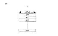
13 スカラーレジスタ(SR)
14 ベクトルレジスタ(VR)
15 マルチプレクサ・デマルチプレクサ(MUX/DEMUX)
16 アドレス生成部
bank0〜bank3 バンク(メモリブロック)
CNT カウント(count:第2パラメータ)
DST ディスタンス(distance:第1パラメータ)
N 同時アクセス可能なバンク(メモリブロック)の数
Claims (5)
- 同時アクセス可能な複数のメモリブロックを有するデータメモリとの間でデータを遣り取りする複数のベクトルパイプラインを有する演算処理装置であって、
前記データメモリに対するストライドアクセスを、基本パターンのデータサイズを決める第1パラメータと、該基本パターンにおける有効なデータ数を決める第2パラメータで規定することを特徴とする演算処理装置。 - 前記第1パラメータをDSTとし、前記第2パラメータをCNTとし、前記同時アクセス可能なメモリブロックの数をNとするとき、DSTおよびCNTは、CNT×N≧DSTを満たす整数として規定されることを特徴とする請求項1に記載の演算処理装置。
- さらに、第1ビット幅を有する第1レジスタを有し、
前記ストライドアクセスにより同時にアクセスされるメモリブロックの数は、前記第1ビット幅に従って規定されることを特徴とする請求項1または2に記載の演算処理装置。 - 前記ストライドアクセスは、ストライドロード/ストア命令によるアクセスであり、
デコードした命令が前記ストライドロード/ストア命令のとき、該ストライドロード/ストア命令の先行命令がロード/ストア命令の場合には、当該先行命令が完了した時点で、前記ストライドロード/ストア命令を前記ベクトルパイプラインへ発行するようになっていることを特徴とする請求項1〜3のいずれか1項に記載の演算処理装置。 - さらに、アドレス生成部を有し、
該アドレス生成部は、前記第1および第2パラメータにより規定される前記基本パターンおよびベースアドレスを受け取って、前記複数のメモリブロックに対するアドレス信号をそれぞれ生成することを特徴とする請求項1〜4のいずれか1項に記載の演算処理装置。
Priority Applications (1)
| Application Number | Priority Date | Filing Date | Title |
|---|---|---|---|
| JP2010278041A JP5664198B2 (ja) | 2010-12-14 | 2010-12-14 | 演算処理装置 |
Applications Claiming Priority (1)
| Application Number | Priority Date | Filing Date | Title |
|---|---|---|---|
| JP2010278041A JP5664198B2 (ja) | 2010-12-14 | 2010-12-14 | 演算処理装置 |
Publications (2)
| Publication Number | Publication Date |
|---|---|
| JP2012128559A true JP2012128559A (ja) | 2012-07-05 |
| JP5664198B2 JP5664198B2 (ja) | 2015-02-04 |
Family
ID=46645529
Family Applications (1)
| Application Number | Title | Priority Date | Filing Date |
|---|---|---|---|
| JP2010278041A Expired - Fee Related JP5664198B2 (ja) | 2010-12-14 | 2010-12-14 | 演算処理装置 |
Country Status (1)
| Country | Link |
|---|---|
| JP (1) | JP5664198B2 (ja) |
Cited By (2)
| Publication number | Priority date | Publication date | Assignee | Title |
|---|---|---|---|---|
| JP2020173609A (ja) * | 2019-04-10 | 2020-10-22 | 日本電気株式会社 | ベクトルプロセッサ装置、生成方法及びプログラム |
| US11200057B2 (en) | 2017-05-15 | 2021-12-14 | Fujitsu Limited | Arithmetic processing apparatus and method for controlling arithmetic processing apparatus |
Citations (2)
| Publication number | Priority date | Publication date | Assignee | Title |
|---|---|---|---|---|
| JPH10134036A (ja) * | 1996-08-19 | 1998-05-22 | Samsung Electron Co Ltd | マルチメディア信号プロセッサの単一命令多重データ処理 |
| JP2010218350A (ja) * | 2009-03-18 | 2010-09-30 | Nec Corp | 情報処理装置 |
-
2010
- 2010-12-14 JP JP2010278041A patent/JP5664198B2/ja not_active Expired - Fee Related
Patent Citations (2)
| Publication number | Priority date | Publication date | Assignee | Title |
|---|---|---|---|---|
| JPH10134036A (ja) * | 1996-08-19 | 1998-05-22 | Samsung Electron Co Ltd | マルチメディア信号プロセッサの単一命令多重データ処理 |
| JP2010218350A (ja) * | 2009-03-18 | 2010-09-30 | Nec Corp | 情報処理装置 |
Cited By (3)
| Publication number | Priority date | Publication date | Assignee | Title |
|---|---|---|---|---|
| US11200057B2 (en) | 2017-05-15 | 2021-12-14 | Fujitsu Limited | Arithmetic processing apparatus and method for controlling arithmetic processing apparatus |
| JP2020173609A (ja) * | 2019-04-10 | 2020-10-22 | 日本電気株式会社 | ベクトルプロセッサ装置、生成方法及びプログラム |
| JP7346883B2 (ja) | 2019-04-10 | 2023-09-20 | 日本電気株式会社 | ベクトルプロセッサ装置及び生成方法 |
Also Published As
| Publication number | Publication date |
|---|---|
| JP5664198B2 (ja) | 2015-02-04 |
Similar Documents
| Publication | Publication Date | Title |
|---|---|---|
| US11714642B2 (en) | Systems, methods, and apparatuses for tile store | |
| EP3629158B1 (en) | Systems and methods for performing instructions to transform matrices into row-interleaved format | |
| JP5658556B2 (ja) | メモリ制御装置、及びメモリ制御方法 | |
| EP4141661B1 (en) | Systems for performing instructions to quickly convert and use tiles as 1d vectors | |
| JP7244046B2 (ja) | 遠隔アトミックオペレーションの空間的・時間的マージ | |
| EP3623941B1 (en) | Systems and methods for performing instructions specifying ternary tile logic operations | |
| KR101597774B1 (ko) | 마스킹된 전체 레지스터 액세스들을 이용한 부분적 레지스터 액세스들을 구현하기 위한 프로세서들, 방법들 및 시스템들 | |
| CN107145335B (zh) | 用于大整数运算的向量指令的装置和方法 | |
| CN104081341B (zh) | 用于多维数组中的元素偏移量计算的指令 | |
| CN108415882B (zh) | 利用操作数基础系统转换和再转换的向量乘法 | |
| EP2962187B1 (en) | Vector register addressing and functions based on a scalar register data value | |
| CN107220029B (zh) | 掩码置换指令的装置和方法 | |
| JP2018504666A (ja) | 多次元アレイから要素の多次元ブロックをプリフェッチするためのハードウェア装置および方法 | |
| US20240143325A1 (en) | Systems, methods, and apparatuses for matrix operations | |
| EP3623940A2 (en) | Systems and methods for performing horizontal tile operations | |
| EP3929733B1 (en) | Matrix transpose and multiply | |
| CN104903867A (zh) | 用于执行冲突检测并将寄存器的内容广播到另一个寄存器的数据元素位置的系统、装置和方法 | |
| CN104350461B (zh) | 具有不同的读和写掩码的多元素指令 | |
| CN113885942A (zh) | 用于将片寄存器对归零的系统和方法 | |
| JP2018500629A (ja) | 3d座標から3dのz曲線インデックスを計算するための機械レベル命令 | |
| CN108369515A (zh) | 用于跨步加载的系统、设备和方法 | |
| JP5664198B2 (ja) | 演算処理装置 | |
| EP3929732A1 (en) | Matrix data scatter and gather by row | |
| CN107168682B (zh) | 用于确定值是否在范围内的指令的装置和方法 |
Legal Events
| Date | Code | Title | Description |
|---|---|---|---|
| A621 | Written request for application examination |
Free format text: JAPANESE INTERMEDIATE CODE: A621 Effective date: 20130904 |
|
| A977 | Report on retrieval |
Free format text: JAPANESE INTERMEDIATE CODE: A971007 Effective date: 20140620 |
|
| A131 | Notification of reasons for refusal |
Free format text: JAPANESE INTERMEDIATE CODE: A131 Effective date: 20140715 |
|
| A521 | Request for written amendment filed |
Free format text: JAPANESE INTERMEDIATE CODE: A523 Effective date: 20140909 |
|
| TRDD | Decision of grant or rejection written | ||
| A01 | Written decision to grant a patent or to grant a registration (utility model) |
Free format text: JAPANESE INTERMEDIATE CODE: A01 Effective date: 20141111 |
|
| A61 | First payment of annual fees (during grant procedure) |
Free format text: JAPANESE INTERMEDIATE CODE: A61 Effective date: 20141124 |
|
| R150 | Certificate of patent or registration of utility model |
Ref document number: 5664198 Country of ref document: JP Free format text: JAPANESE INTERMEDIATE CODE: R150 |
|
| LAPS | Cancellation because of no payment of annual fees |