JP2012129152A - Lighting device and projector - Google Patents
Lighting device and projector Download PDFInfo
- Publication number
- JP2012129152A JP2012129152A JP2010281838A JP2010281838A JP2012129152A JP 2012129152 A JP2012129152 A JP 2012129152A JP 2010281838 A JP2010281838 A JP 2010281838A JP 2010281838 A JP2010281838 A JP 2010281838A JP 2012129152 A JP2012129152 A JP 2012129152A
- Authority
- JP
- Japan
- Prior art keywords
- frequency
- capacitor
- conversion circuit
- circuit
- current
- Prior art date
- Legal status (The legal status is an assumption and is not a legal conclusion. Google has not performed a legal analysis and makes no representation as to the accuracy of the status listed.)
- Granted
Links
- 239000003990 capacitor Substances 0.000 claims abstract description 195
- 238000006243 chemical reaction Methods 0.000 claims abstract description 171
- 238000004804 winding Methods 0.000 claims abstract description 109
- 238000012544 monitoring process Methods 0.000 claims description 33
- 230000003287 optical effect Effects 0.000 claims description 26
- 238000005286 illumination Methods 0.000 claims description 11
- 238000007599 discharging Methods 0.000 claims description 8
- 230000004907 flux Effects 0.000 claims description 2
- 238000010586 diagram Methods 0.000 description 18
- 238000000034 method Methods 0.000 description 15
- 230000008569 process Effects 0.000 description 15
- 230000015556 catabolic process Effects 0.000 description 12
- 239000004973 liquid crystal related substance Substances 0.000 description 12
- 230000008859 change Effects 0.000 description 5
- 230000004048 modification Effects 0.000 description 5
- 238000012986 modification Methods 0.000 description 5
- 230000000694 effects Effects 0.000 description 4
- 230000008878 coupling Effects 0.000 description 3
- 238000010168 coupling process Methods 0.000 description 3
- 238000005859 coupling reaction Methods 0.000 description 3
- 230000007423 decrease Effects 0.000 description 3
- 238000007789 sealing Methods 0.000 description 3
- 230000009471 action Effects 0.000 description 2
- 230000003321 amplification Effects 0.000 description 2
- 238000001816 cooling Methods 0.000 description 2
- 230000005669 field effect Effects 0.000 description 2
- 238000012423 maintenance Methods 0.000 description 2
- QSHDDOUJBYECFT-UHFFFAOYSA-N mercury Chemical compound [Hg] QSHDDOUJBYECFT-UHFFFAOYSA-N 0.000 description 2
- 229910052753 mercury Inorganic materials 0.000 description 2
- 238000003199 nucleic acid amplification method Methods 0.000 description 2
- 238000012545 processing Methods 0.000 description 2
- 230000004044 response Effects 0.000 description 2
- 238000000926 separation method Methods 0.000 description 2
- 239000000126 substance Substances 0.000 description 2
- 238000009825 accumulation Methods 0.000 description 1
- 239000000853 adhesive Substances 0.000 description 1
- 230000001070 adhesive effect Effects 0.000 description 1
- 230000002411 adverse Effects 0.000 description 1
- 238000003491 array Methods 0.000 description 1
- 230000008901 benefit Effects 0.000 description 1
- 230000003111 delayed effect Effects 0.000 description 1
- 230000006866 deterioration Effects 0.000 description 1
- 239000011521 glass Substances 0.000 description 1
- 238000009413 insulation Methods 0.000 description 1
- 229910052751 metal Inorganic materials 0.000 description 1
- 239000002184 metal Substances 0.000 description 1
- 230000010355 oscillation Effects 0.000 description 1
- 230000010287 polarization Effects 0.000 description 1
- 238000010992 reflux Methods 0.000 description 1
- 230000000630 rising effect Effects 0.000 description 1
- 239000004065 semiconductor Substances 0.000 description 1
- 230000008054 signal transmission Effects 0.000 description 1
- 230000002194 synthesizing effect Effects 0.000 description 1
- 229920003002 synthetic resin Polymers 0.000 description 1
- 239000000057 synthetic resin Substances 0.000 description 1
Images





Landscapes
- Circuit Arrangements For Discharge Lamps (AREA)
Abstract
【課題】簡易な構成で放電灯に対する高電圧パルスの印加タイミングを設定できるようにする。
【解決手段】点灯装置52では、放電灯511の点灯の際に、変換回路72を低周波駆動する期間と、高周波駆動する期間の切り替えを行う。この低周波駆動の期間においては、ハイパスフィルター740から電流出力部750に電流が流れず、サイリスターX1のOFF状態が維持され、コンデンサーC1に電荷が充電される。そして、コンデンサーC1への充電完了後に、変換回路72を高周波駆動に切り替え、ハイパスフィルター740から電流出力部750に電流を流すことによりサイリスターX1をON(導通)にし、コンデンサーC1に蓄積された電荷を一次巻線7011を通して放電する。この一次巻線7011に流れる電流により二次巻線7012側に高電圧パルスを発生させ、この高電圧パルスを放電灯511の電極Eに印加する。
【選択図】図2The application timing of a high voltage pulse to a discharge lamp can be set with a simple configuration.
A lighting device 52 switches between a period during which a conversion circuit 72 is driven at a low frequency and a period during which it is driven at a high frequency when the discharge lamp 511 is turned on. During this low frequency drive period, no current flows from the high-pass filter 740 to the current output unit 750, the thyristor X1 is maintained in the OFF state, and the capacitor C1 is charged. Then, after the charging of the capacitor C1 is completed, the conversion circuit 72 is switched to high frequency driving, and a current is passed from the high pass filter 740 to the current output unit 750 so that the thyristor X1 is turned on (conduction), and the charge accumulated in the capacitor C1 is changed. Discharge through primary winding 7011. A high voltage pulse is generated on the secondary winding 7012 side by the current flowing through the primary winding 7011, and this high voltage pulse is applied to the electrode E of the discharge lamp 511.
[Selection] Figure 2
Description
本発明は、放電灯を点灯させる点灯装置、及び該点灯装置を備えるプロジェクターに関する。 The present invention relates to a lighting device for lighting a discharge lamp, and a projector including the lighting device.
従来、光源と、当該光源から出射される光束を変調して、画像情報に応じた画像を形成する光変調装置と、当該画像を投射する投射光学装置とを備えたプロジェクターが知られている。このような光源として、内部に一対の電極及び放電物質が封入される放電空間が形成された超高圧水銀ランプ等の放電灯が採用されることが多く、この場合には、当該放電灯の点灯を制御する点灯装置が採用される。このような点灯装置として、放電灯にランプ電力を供給して当該放電灯を点灯させる点灯装置と、当該点灯装置の駆動を制御する制御装置とを備えたものが知られている(例えば、特許文献1参照)。 2. Description of the Related Art Conventionally, a projector is known that includes a light source, a light modulation device that modulates a light beam emitted from the light source, and forms an image according to image information, and a projection optical device that projects the image. As such a light source, a discharge lamp such as an ultra-high pressure mercury lamp in which a discharge space in which a pair of electrodes and a discharge substance are enclosed is formed is often used. In this case, the discharge lamp is turned on. A lighting device that controls the lighting is employed. As such a lighting device, a device including a lighting device that supplies lamp power to a discharge lamp to light the discharge lamp and a control device that controls driving of the lighting device is known (for example, a patent). Reference 1).
この特許文献1に記載の点灯装置では、出力電流及び出力電力を調整する変換回路と、直流電流を交流電流に変換するインバーター回路と、イグナイター回路と、当該イグナイター回路に接続される一次巻線、及び、インバーター回路に接続される二次巻線を有するトランスと、当該各回路を複数の駆動回路を介して制御する制御回路(マイクロコンピューター)とを備える。そして、この点灯装置では、当該制御回路が駆動回路にシグナルを出力することで、イグナイター回路が高電圧のイグニッションパルスをトランスの一次巻線に供給する。これにより、当該トランスの二次巻線に生じた高電圧パルスが、放電灯に印加され、当該放電灯にて放電が開始される。
In the lighting device described in
しかしながら、前述の特許文献1に記載の点灯装置では、制御回路及び駆動回路とイグナイター回路とが制御線で接続されているため、当該制御線に高電圧が印加される可能性があり、これにより、制御回路が損傷する場合がある。このため、制御回路に耐高電圧対策を施す必要があり、点灯制御回路の構成が複雑化するという問題がある。
However, in the lighting device described in
本発明の目的は、簡易な構成により放電灯に対する高電圧パルスの印加タイミングを設定できる点灯装置、及びプロジェクターを提供することにある。 The objective of this invention is providing the lighting device and projector which can set the application timing of the high voltage pulse with respect to a discharge lamp with simple structure.
前記した目的を達成するために、本発明の点灯装置は、放電灯の電極に電力を供給して、前記放電灯を点灯させる点灯装置であって、それぞれ直流電流が入力される一対の第1スイッチング素子及び一対の第2スイッチング素子を有し、前記一対の第1スイッチング素子及び前記一対の第2スイッチング素子のうちの一方が導通状態となり他方が非導通状態となる状態変化が交互に切り替わることで、前記直流電流を交流電流に変換する変換回路と、前記変換回路から入力される交流電流から高電圧パルスを生成し、当該高電圧パルスを前記電極に印加するパルス生成回路と、前記パルス生成回路に前記高電圧パルスを生成させるトリガー回路と、前記直流電流により電荷が蓄積されるコンデンサーと、を備え、前記パルス生成回路は、前記トリガー回路に接続される一次巻線と、前記変換回路に接続される二次巻線とを備えるトランスを有し、前記一次巻線に入力される電流に応じて、前記二次巻線に入力される電流を昇圧して前記高電圧パルスを生成し、前記トリガー回路は、前記第1スイッチング素子と前記第2スイッチング素子の接続点である中点と接続され、前記変換回路から所定周波数以上の交流電流が入力されると当該交流電流を導通させ、前記所定周波数未満の交流電流が入力されると当該交流電流を遮断するハイパスフィルターと、前記ハイパスフィルターを介して前記所定周波数以上の交流電流が入力された場合、前記コンデンサーに蓄積された電荷を放電させることにより前記一次巻線に電流を流す第3スイッチング素子と、を有することを特徴とする。 In order to achieve the above-described object, the lighting device of the present invention is a lighting device that turns on the discharge lamp by supplying electric power to the electrode of the discharge lamp, each of which is supplied with a direct current. A switching element and a pair of second switching elements, wherein a state change in which one of the pair of first switching elements and the pair of second switching elements is in a conductive state and the other is in a non-conductive state is alternately switched; A conversion circuit for converting the direct current into an alternating current, a pulse generation circuit for generating a high voltage pulse from the alternating current input from the conversion circuit, and applying the high voltage pulse to the electrode, and the pulse generation A trigger circuit that causes the circuit to generate the high-voltage pulse, and a capacitor in which electric charge is accumulated by the direct current, the pulse generation circuit, A transformer having a primary winding connected to a rigger circuit and a secondary winding connected to the conversion circuit, and input to the secondary winding in accordance with a current input to the primary winding; The trigger circuit is connected to a midpoint that is a connection point between the first switching element and the second switching element, and has a predetermined frequency or more from the conversion circuit. When an alternating current is input, the alternating current is conducted, and when an alternating current of less than the predetermined frequency is input, a high-pass filter that cuts off the alternating current, and an alternating current of the predetermined frequency or higher is passed through the high-pass filter. And a third switching element that causes a current to flow through the primary winding by discharging the charge accumulated in the capacitor.
なお、第1スイッチング素子及び第2スイッチングとしては、バイポーラトランジスターの他、FET(Field Effect Transistor)を例示でき、また、FETとしては、MOSFET(Metal−Oxide−Semiconductor FET)等を例示できる。さらには、IGBT(Insulated Gate Bipolar Transistor)を例示できる。 In addition, as a 1st switching element and 2nd switching, FET (Field Effect Transistor) can be illustrated other than a bipolar transistor, Moreover, MOSFET (Metal-Oxide-SemiconductorFET) etc. can be illustrated as FET. Furthermore, an IGBT (Insulated Gate Bipolar Transistor) can be exemplified.
本発明によれば、放電灯の点灯始動時において、変換回路を所定周波数未満の周波数により低周波駆動する低周波期間と、所定周波数以上の周波数により高周波駆動する高周波期間との間で切り替えができるようにする。ここで高周波駆動とは、ハイパスフィルターを導通する交流電流の周波数(所定周波数以上の周波数)で変換回路を駆動することを意味する。また、低周波駆動とは、ハイパスフィルターを導通させない交流電流の周波数(所定周波数未満の周波数)で変換回路を駆動することを意味する。なお、ハイパスフィルターを導通にする交流電流の周波数と、ハイパスフィルターを非導通にする交流電流の周波数とを区分する基準となる周波数(前述の所定周波数)を「導通周波数」と呼ぶことがあり、また、ハイパスフィルターを導通する交流電流(所定周波数以上の交流電流)を「高周波電流」と呼ぶことがある。
そして、上記変換回路の低周波期間においては、ハイパスフィルターが非導通となり第3スイッチング素子がOFF(非導通)状態となるので、この低周波期間においてコンデンサーを充電する。そして、低周波期間においてコンデンサーへの充電を完了させた後に、変換回路を高周波駆動に切り替え、ハイパスフィルターに高周波電流(所定周波数以上の交流電流)を導通させることにより第3スイッチング素子をON(導通)にする。この第3スイッチング素子をONにすることにより、コンデンサーに蓄積された電荷をトランスの一次巻線を通して放電し、一次巻線に電流を流すことによりパルス生成回路(二次巻線)より高電圧パルスを発生させ、この高電圧パルスを放電灯の電極に印加する。
According to the present invention, at the time of starting the discharge lamp, it is possible to switch between a low frequency period in which the conversion circuit is driven at a low frequency with a frequency less than a predetermined frequency and a high frequency period in which the conversion circuit is driven at a high frequency with a frequency higher than the predetermined frequency. Like that. Here, the high-frequency driving means that the conversion circuit is driven at a frequency of an alternating current (a frequency equal to or higher than a predetermined frequency) that conducts the high-pass filter. The low frequency drive means that the conversion circuit is driven at a frequency of an alternating current (a frequency less than a predetermined frequency) that does not cause the high-pass filter to conduct. In addition, the frequency (the aforementioned predetermined frequency) that serves as a reference for distinguishing the frequency of the alternating current that makes the high-pass filter conductive and the frequency of the alternating current that makes the high-pass filter nonconductive may be referred to as a “conduction frequency”. In addition, an alternating current (an alternating current having a predetermined frequency or higher) that conducts the high pass filter may be referred to as a “high-frequency current”.
In the low-frequency period of the conversion circuit, the high-pass filter is non-conductive and the third switching element is in the OFF (non-conductive) state. Therefore, the capacitor is charged in this low-frequency period. Then, after completing the charging of the capacitor in the low frequency period, the conversion circuit is switched to high frequency driving, and the third switching element is turned on (conduction) by conducting high frequency current (AC current of a predetermined frequency or higher) to the high pass filter. ). By turning on the third switching element, the electric charge accumulated in the capacitor is discharged through the primary winding of the transformer, and a current is passed through the primary winding to cause a higher voltage pulse than the pulse generation circuit (secondary winding). And this high voltage pulse is applied to the electrode of the discharge lamp.
ここで、コンデンサーに電荷を蓄積するために必要な充電期間は、当該コンデンサーの静電容量及び充電時定数により算出することができる。このため、コンデンサーへの充電に必要な期間が経過した後は、任意のタイミッグで変換回路を高周波駆動することで、高電圧パルスを出力できる。従って、所望のタイミングで高電圧パルスを放電灯の電極に印加できる。 Here, the charging period necessary for accumulating the charge in the capacitor can be calculated from the capacitance of the capacitor and the charging time constant. For this reason, after a period necessary for charging the capacitor has elapsed, a high voltage pulse can be output by driving the conversion circuit at a high frequency with an arbitrary timing. Therefore, a high voltage pulse can be applied to the electrode of the discharge lamp at a desired timing.
これにより、前述の特許文献1に記載の点灯装置のように、制御装置(制御回路及び駆動回路)とイグナイター回路とを制御線で接続して、イグナイター回路による高電圧パルスの印加タイミングを制御する必要がなく、制御装置における耐高電圧対策が緩和される。これにより、簡易な構成により放電灯に対する高電圧パルスの印加タイミングを設定できる点灯装置を提供することができる。
Thereby, like the lighting device described in
また、本発明の点灯装置では、前記第3スイッチング素子は、前記ハイパスフィルターを介して入力される交流電流により駆動される第1トランジスターと、前記第1トランジスターにより駆動される第2トランジスターと、前記第2トランジスターにより制御されるゲート、前記コンデンサーの一端に前記一次巻線を介して接続されるアノード、及び前記コンデンサーの他端に接続されるカソードを有するサイリスターと、を備え、前記第1トランジスターが前記ハイパスフィルターを介して入力される交流電流により駆動された場合に、前記サイリスターが導通となり前記コンデンサーに蓄積された電荷を放電させることにより前記一次巻線に電流を流すことを特徴とする。 In the lighting device of the present invention, the third switching element includes a first transistor driven by an alternating current input through the high-pass filter, a second transistor driven by the first transistor, A thyristor having a gate controlled by a second transistor, an anode connected to one end of the capacitor via the primary winding, and a cathode connected to the other end of the capacitor, wherein the first transistor comprises: When driven by an alternating current input through the high-pass filter, the thyristor becomes conductive, and a current is passed through the primary winding by discharging the charge accumulated in the capacitor.
本発明によれば、第3スイッチング素子が、トランジスター及びサイリスターで構成されていることにより、変換回路が低周波駆動から高周波駆動に切り替わった際に、速やかに応答してコンデンサーの電荷放出を行い、一次巻線に電流を供給することができる。従って、コンデンサーの電荷の充電完了から高電圧パルスの発生までの期間を短縮することができる。また、任意のタイミングで高電圧パルスを確実に印加できる。また、このようなサイリスターは大電流を導通させることができるので、コンデンサーの静電容量が大きくても、このコンデンサーの放電電流を確実に導通させることができる。 According to the present invention, since the third switching element is constituted by a transistor and a thyristor, when the conversion circuit is switched from the low frequency drive to the high frequency drive, the capacitor is discharged quickly in response. A current can be supplied to the primary winding. Therefore, it is possible to shorten the period from the completion of charging the capacitor charge to the generation of the high voltage pulse. Moreover, a high voltage pulse can be applied reliably at an arbitrary timing. In addition, since such a thyristor can conduct a large current, even if the capacitance of the capacitor is large, the discharge current of the capacitor can be reliably conducted.
また、本発明の点灯装置は、前記一対の第1スイッチング素子及び前記一対の第2スイッチング素子の導通状態及び非導通状態を制御する制御信号を出力して、前記変換回路を駆動させる制御部を備えることを特徴とする。 The lighting device according to the present invention further includes a control unit that drives the conversion circuit by outputting a control signal for controlling a conduction state and a non-conduction state of the pair of first switching elements and the pair of second switching elements. It is characterized by providing.
本発明によれば、前述の点灯装置と同様の効果を奏することができるほか、制御部が変換回路に制御信号を出力することで、第1スイッチング素子及び第2スイッチング素子の導通状態及び非導通状態を確実に制御でき、ひいては、変換回路を高周波(所定周波数以上の周波数)及び低周波(所定周波数未満の周波数)で駆動させることができる。従って、コンデンサーを充電する場合と、高電圧パルスを発生及び印加させる場合と、を適切に制御できる。また、高電圧パルスの発生及び印加を高い頻度で行うようにして放電灯の点灯を促進したり、或いは、低い頻度で行うようにして回路素子の劣化を抑制し、点灯装置の長寿命化を図ることも可能となる。 According to the present invention, the same effect as that of the above-described lighting device can be obtained, and the control unit outputs a control signal to the conversion circuit, whereby the first switching element and the second switching element are turned on and off. The state can be reliably controlled, and as a result, the conversion circuit can be driven at a high frequency (frequency higher than a predetermined frequency) and a low frequency (frequency lower than the predetermined frequency). Therefore, it is possible to appropriately control the case where the capacitor is charged and the case where the high voltage pulse is generated and applied. In addition, high voltage pulses are generated and applied at a high frequency to promote the lighting of the discharge lamp, or at a low frequency to suppress the deterioration of circuit elements and extend the life of the lighting device. It is also possible to plan.
また、本発明の点灯装置は、前記制御部は、前記パルス生成回路により前記高電圧パルスを前記電極に印加するタイミングに基づいて、前記変換回路の駆動周波数を、前記所定周波数より低い第2周波数から前記所定周波数以上の第1周波数に切り替えることを特徴とする。 Further, in the lighting device of the present invention, the control unit sets the drive frequency of the conversion circuit to a second frequency lower than the predetermined frequency based on the timing at which the pulse generation circuit applies the high voltage pulse to the electrodes. To the first frequency equal to or higher than the predetermined frequency.
本発明によれば、制御部が、所定周波数より低い周波数(導通周波数未満の周波数)である第2周波数で変換回路を駆動することで、変換回路から出力される交流電流がハイパスフィルターを導通しないようにして(第3スイッチング素子を非導通にして)、コンデンサーを充電する。そして、コンデンサーの充電完了後に、所定周波数以上(導通周波数以上)の周波数である第1周波数に変換回路の駆動周波数を変更することで、コンデンサーに蓄積された電荷を放電させて一次巻線に電流を流し、二次巻線に発生した高電圧パルスを放電灯の電極に印加する。そして、制御部が、第2周波数での変換回路の駆動と、第1周波数での変換回路の駆動とを、高電圧パルスの印加タイミングに基づいて切り替えることで、任意のタイミングで、電極に高電圧パルスを印加することができる。 According to the present invention, the controller drives the conversion circuit at the second frequency that is lower than the predetermined frequency (frequency less than the conduction frequency), so that the alternating current output from the conversion circuit does not conduct the high-pass filter. In this way (the third switching element is turned off), the capacitor is charged. Then, after completing the charging of the capacitor, by changing the driving frequency of the conversion circuit to the first frequency that is a predetermined frequency or higher (conducting frequency or higher), the electric charge accumulated in the capacitor is discharged and the primary winding becomes a current. The high voltage pulse generated in the secondary winding is applied to the electrode of the discharge lamp. Then, the control unit switches the driving of the conversion circuit at the second frequency and the driving of the conversion circuit at the first frequency based on the application timing of the high voltage pulse, so that the high voltage is applied to the electrode at an arbitrary timing. A voltage pulse can be applied.
このような制御部による変換回路の駆動周波数の切替(第1周波数と第2周波数との切替)は、各第1スイッチング素子及び各第2スイッチング素子にゲート電圧を印加する周波数を変更することにより行うことができるので、当該制御部の構成を簡易な構成とすることができる。従って、簡易な構成で高電圧パルスの印加タイミングを確実に設定できる。 Switching of the driving frequency of the conversion circuit by the control unit (switching between the first frequency and the second frequency) is performed by changing the frequency at which the gate voltage is applied to each first switching element and each second switching element. Since it can be performed, the structure of the said control part can be made into a simple structure. Therefore, the application timing of the high voltage pulse can be reliably set with a simple configuration.
また、本発明の点灯装置は、前記制御部は、前記変換回路の駆動周波数を前記第2周波数で所定の時間駆動させた後、前記第1周波数に切り替えることを特徴とする。 Further, the lighting device of the present invention is characterized in that the control unit switches the driving frequency of the conversion circuit to the first frequency after driving the driving frequency at the second frequency for a predetermined time.
本発明によれば、制御部が、第2周波数で変換回路を所定時間駆動してコンデンサーへの充電を完了させる。その後に、変換回路を第1周波数で駆動し、コンデンサーに蓄積された電荷を放電させることにより一次巻線に電流を流し、二次巻線に発生した高電圧パルスを放電灯の電極Eに印加する。
これにより、変換回路を第2周波数で所定時間駆動してコンデンサーを充電できる。そして、変換回路の駆動周波数を第1周波数に変更し、コンデンサーに蓄積された電荷を放電させることにより一次巻線に電流を流し、高電圧パルスを発生させて放電灯の電極に印加することができる。このため、簡易な構成で高電圧パルスの印加タイミングを確実に設定できる。
According to the present invention, the control unit drives the conversion circuit at the second frequency for a predetermined time to complete the charging of the capacitor. After that, the conversion circuit is driven at the first frequency, the electric charge accumulated in the capacitor is discharged, the current flows through the primary winding, and the high voltage pulse generated in the secondary winding is applied to the electrode E of the discharge lamp. To do.
Accordingly, the capacitor can be charged by driving the conversion circuit at the second frequency for a predetermined time. Then, the drive frequency of the conversion circuit is changed to the first frequency, and the electric charge accumulated in the capacitor is discharged to cause a current to flow through the primary winding, thereby generating a high voltage pulse and applying it to the electrode of the discharge lamp. it can. For this reason, the application timing of the high voltage pulse can be reliably set with a simple configuration.
また、本発明の点灯装置は、前記一対の第1スイッチング素子及び前記一対の第2スイッチング素子の導通状態及び非導通状態を制御する制御信号を出力して、前記変換回路を駆動させる制御部を備え、前記制御部は、前記放電灯の点灯始動時に前記変換回路を常に前記所定周波数以上の周波数で駆動させ、前記トリガー回路は、前記第1トランジスターに対して、前記ハイパスフィルターを介して入力される前記交流電流を入力するか、または前記第1トランジスターをオフさせる電圧を印加するか、を切り替える電圧監視回路を備え、前記電圧監視回路は、前記コンデンサーの電圧が所定電圧より低い場合、前記第1トランジスターをオフさせる制御をし、前記コンデンサーの電圧が所定電圧以上の場合、前記ハイパスフィルターを介して入力される前記交流電流を前記第1トランジスターに入力させる制御をすることを特徴とする。 The lighting device according to the present invention further includes a control unit that drives the conversion circuit by outputting a control signal for controlling a conduction state and a non-conduction state of the pair of first switching elements and the pair of second switching elements. And the control unit always drives the conversion circuit at a frequency equal to or higher than the predetermined frequency when the discharge lamp starts lighting, and the trigger circuit is input to the first transistor via the high-pass filter. A voltage monitoring circuit for switching whether to input the alternating current to be applied or to apply a voltage for turning off the first transistor, and the voltage monitoring circuit, when the voltage of the capacitor is lower than a predetermined voltage, When one capacitor is controlled to turn off and the voltage of the capacitor is higher than a predetermined voltage, the high-pass filter is used. The alternating current input, characterized in that the control for input to the first transistor.
本発明によれば、放電灯の点灯始動時において、制御部が、変換回路を常に所定周波数以上(導通周波以上)の周波数で駆動し、電圧監視回路が、コンデンサーの充電電圧を監視する。そして、コンデンサーの充電電圧が所定の電圧値以上になったことを検出して、ハイパスフィルターから入力される高周波電流(所定周波数以上の交流電流)を第1トランジスターに流すことによりサイリスターを導通にし、コンデンサーに蓄積された電荷を放電して一次巻線に電流を流し、二次巻線に発生した高電圧パルスを放電灯の電極に印加する。
これにより、放電灯の点灯始動時において、変換回路における駆動周波数の切り替えの必要がなくなる。また、高電圧パルスの発生のタイミングを電圧監視回路により自動で検出して制御できる。このため、コンデンサーの充電開始から高電圧パルスの発生までの期間を短縮することができる。
According to the present invention, at the start of lighting of the discharge lamp, the control unit always drives the conversion circuit at a frequency equal to or higher than a predetermined frequency (conductive frequency or higher), and the voltage monitoring circuit monitors the charging voltage of the capacitor. And it detects that the charging voltage of the capacitor has become a predetermined voltage value or more, makes the thyristor conductive by flowing a high-frequency current (AC current of a predetermined frequency or more) input from the high-pass filter to the first transistor, The electric charge accumulated in the capacitor is discharged to pass a current through the primary winding, and a high voltage pulse generated in the secondary winding is applied to the electrode of the discharge lamp.
This eliminates the need to switch the driving frequency in the conversion circuit when the discharge lamp is turned on. Further, the timing of generation of the high voltage pulse can be automatically detected and controlled by the voltage monitoring circuit. For this reason, the period from the start of charging the capacitor to the generation of the high voltage pulse can be shortened.
また、本発明のプロジェクターは、上記の何れかに記載の点灯装置と、前記点灯装置により供給される電力により点灯される放電灯と、前記放電灯を有する照明装置から出射された光束を変調する光変調装置と、変調された前記光束を投射する投射光学装置と、を備えることを特徴とする。 According to another aspect of the invention, there is provided a projector for modulating a light beam emitted from the lighting device according to any one of the above, a discharge lamp that is turned on by power supplied from the lighting device, and a lighting device having the discharge lamp. A light modulation device and a projection optical device that projects the modulated light beam.
本発明によれば、前述の点灯装置と同様の効果を奏することができる。また、前述のように、不要な高電圧パルスの電極に対する印加を抑制できるので、放電灯の長寿命化、ひいては、照明装置の長寿命化を図れる。更には、放電灯の交換等のプロジェクターのメンテナンスを簡略化できる。 According to the present invention, the same effects as those of the lighting device described above can be obtained. Further, as described above, since it is possible to suppress the application of unnecessary high voltage pulses to the electrodes, it is possible to extend the life of the discharge lamp, and hence the life of the lighting device. Furthermore, maintenance of the projector such as replacement of the discharge lamp can be simplified.
以下、本発明の一実施形態を図面に基づいて説明する。 Hereinafter, an embodiment of the present invention will be described with reference to the drawings.
[第1の実施形態]
まず、本発明の実施形態に係る点灯装置52が用いられるプロジェクター1の構成について説明する。
[First Embodiment]
First, the configuration of the
図1は、本実施形態に係るプロジェクター1の構成を示す模式図である。
図1において、プロジェクター1は、内部に設けられた光源から出射された光束を変調して、画像情報に応じた画像を形成し、当該画像をスクリーン等の被投射面上に拡大投射するものである。このプロジェクター1は、図1に示すように、外装筐体2、投射光学装置3及び画像形成装置4を備える。この他、プロジェクター1は、当該プロジェクター1内部を冷却する冷却ファン等で構成される冷却ユニット91、商用交流電流を変換した直流電流をプロジェクター1内部の各構成部材に供給する電源ユニット92、及び、プロジェクター1全体を制御する制御ユニット93等を備える。
外装筐体2は、合成樹脂又は金属により全体略直方体状に形成された筐体であり、前述の各装置3,4及び各ユニット91〜93等を内部に収納する。投射光学装置3は、後述する画像形成装置4にて形成された画像を被投射面上に結像させるとともに、当該画像を拡大投射する。この投射光学装置3は、図示を省略するが、筒状の鏡筒内に複数のレンズが収納された組レンズとして構成されている。
画像形成装置4は、前述の制御ユニット93による制御の下、画像情報に応じた画像を形成する光学装置である。この画像形成装置4は、照明装置5、照明光学装置41、色分離光学装置42、リレー光学装置43及び電気光学装置44を備え、これらを内部に設定された照明光軸A上の所定位置に収納配置するほか、投射光学装置3を支持する光学部品用筐体45を備える。
FIG. 1 is a schematic diagram illustrating a configuration of a
In FIG. 1, a
The
The image forming apparatus 4 is an optical apparatus that forms an image according to image information under the control of the
照明装置5は、光束を出射する。この照明装置5の構成は、後に詳述する。
照明光学装置41は、一対のレンズアレイ411,412、偏光変換素子413及び重畳レンズ414を備える。色分離光学装置42は、ダイクロイックミラー421,422及び反射ミラー423を備え、リレー光学装置43は、入射側レンズ431、リレーレンズ433及び反射ミラー432,434を備える。電気光学装置44は、フィールドレンズ441と、光変調装置としての3つの液晶パネル442(赤色光用、緑色光用及び青色光用の液晶パネルを、それぞれ442R,442G,442Bとする)と、それぞれ3つの入射側偏光板443、視野角補償板444及び出射側偏光板445と、色合成光学装置としてのクロスダイクロイックプリズム446とを備える。
The illumination device 5 emits a light beam. The configuration of the illumination device 5 will be described in detail later.
The illumination
このような画像形成装置4では、照明光学装置41により、照明装置5(光源装置51)から出射された光束の照明領域内の照度が略均一化され、当該光束は、色分離光学装置42により、赤(R),緑(G),青(B)の3つの色光に分離される。これら分離された各色光は、各液晶パネル442にて画像情報に応じてそれぞれ変調され、色光毎の画像が形成される。そして、当該色光毎の画像は、クロスダイクロイックプリズム446にて合成され、投射光学装置3により被投射面上に拡大投射される。
In such an image forming apparatus 4, the illumination
(照明装置の構成)
照明装置5は、光源としての放電灯511、主反射鏡512、副反射鏡513、平行化レンズ514、及び、これらを内部に収納するハウジング515を有する光源装置51と、放電灯511の点灯を制御する点灯装置52とを備える。このうち、放電灯511は、内部に形成された放電空間内に一対の電極E(E1,E2)(図2参照)及び放電物質が封入された略球状を有する発光部5111と、当該発光部5111の両端から互いに離間する方向に延出する一対の封止部5112,5113とを有する。このような放電灯511として、例えば、超高圧水銀ランプ等を採用できる。
(Configuration of lighting device)
The illuminating device 5 includes a
主反射鏡512は、レンズアレイ411から離間する側の封止部5112に接着剤により固定される。この主反射鏡512の内側には、凹曲面状の反射面が形成されており、当該反射面により発光部5111から入射された光を反射させて、照明光軸A上の第2焦点に収束させる。副反射鏡513は、発光部5111における封止部5113側(主反射鏡512側とは反対側)を覆うガラス製の成形品である。この副反射鏡513は、発光部5111の外形に沿う形状を有し、当該発光部5111と対向する面には、反射面が形成されている。そして、副反射鏡513は、発光部5111から出射された光のうち、主反射鏡512側とは反対側に射出された光を、当該反射面により反射させて、主反射鏡512の反射面に入射させる。これにより、発光部5111から光源装置51の光束出射方向の先端側に直接射出され、かつ、レンズアレイ411に入射しない光の発生を抑えることができる。平行化レンズ514は、主反射鏡512にて反射されて収束される光束を照明光軸Aに対して平行化する。
The main reflecting
(点灯装置の構成)
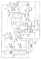
図2は、本発明の実施形態に係わる点灯装置52の構成を示す図である。点灯装置52は、図2に示すように、前述の電源ユニット92から供給される直流電流を交流電流に変換して放電灯511の電極E(E1,E2)に出力し、当該放電灯511を点灯させる駆動回路部7と、前述の制御ユニット93の制御下で駆動回路部7を制御する制御部6とを備える。
(Configuration of lighting device)
FIG. 2 is a diagram showing a configuration of the
駆動回路部7は、降圧回路71、変換回路72、パルス生成回路73及びトリガー回路74を備えるほか、抵抗R1,R2及びコンデンサー(キャパシター)C1を備える。
降圧回路71は、ダウンチョッパー回路であり、制御部6による制御の下、電源ユニット92に接続される直流電源Vinから入力される略380Vの直流電圧を、放電灯511の点灯に適した電圧(例えば、略50V〜150V)に降下させる回路である。この降圧回路71は、詳しい図示を省略するが、例えば、直列接続されるスイッチング素子としてのFET(Field Effect Transistor)及びコイルと、これらの素子から分岐して接続されるダイオード及びコンデンサーとを備える。これらのうち、FETは、制御部6により印加されるゲート電圧に応じて、入力される放電灯511への直流電流を制御して、放電灯511に供給される電力を一定に保つ。また、コイル、ダイオード及びコンデンサーは、入力される直流電流の高周波成分の除去、整流及び定電力化を行う。そして、後述する制御部6が、ランプの点灯状態に応じて当該ゲート電圧のパルスデューティ比を制御することで、降圧回路71は、放電灯511の点灯時にランプ電流を出力する。
なお、降圧回路71の出力端は制御部6と接続され、当該制御部6により、降圧回路71から変換回路72に入力される電流値及び電圧値が検出される。
The drive circuit unit 7 includes a step-
The step-
The output terminal of the step-
(変換回路72の構成)
変換回路72は、インバーター回路であり、入力される直流電流を交流電流に変換する。この変換回路72は、Nチャネル型のMOSFET(Metal−Oxide−Semiconductor FET)721(S1)、MOSFET722(S2)、MOSFET723(S3)、及びMOSFET724(S4)を備えたインバーターブリッジ回路として構成されている。このブリッジ回路は、ハイサイド側のMOSFET721(S1)とMOSFET723(S3)のそれぞれのドレインが降圧回路71の正(+)側の出力端子に接続され、ローサイド側のMOSFET722(S2)とMOSFET724(S4)のそれぞれのソースが降圧回路71の負(−)側の出力端子に接続される。また、MOSFET721(S1)とソースと、MOSFET722(S2)のドレインとがノードN1により接続され、同様にMOSFET723(S3)とソースと、MOSFET724(S4)のドレインとがノードN2により接続される。
(Configuration of Conversion Circuit 72)
The
なお、このブリッジ回路において、本発明における一対の第1スイッチング素子は、MOSFET721(S1)とMOSFET724(S4)とが対応し、一対の第2スイッチング素子は、MOSFET722(S2)とMOSFET723(S3)とが対応する。さらに、本発明における第1スイッチング素子と第2スイッチング素子の接続点である中点は、MOSFET721(S1)のソースとMOSFET722(S2)のドレインとの接続点(ノードN1)、或いは、MOSFET723(S3)のソースとMOSFET724(S4)のドレインとの接続点(ノードN2)が対応する。 In this bridge circuit, the pair of first switching elements in the present invention corresponds to the MOSFET 721 (S1) and the MOSFET 724 (S4), and the pair of second switching elements includes the MOSFET 722 (S2) and the MOSFET 723 (S3). Corresponds. Further, the midpoint, which is the connection point between the first switching element and the second switching element in the present invention, is the connection point (node N1) between the source of the MOSFET 721 (S1) and the drain of the MOSFET 722 (S2) or the MOSFET 723 (S3). ) And the connection point (node N2) between the drain of MOSFET 724 (S4).
このブリッジ回路には、降圧回路71を経て整流された直流電流が入力される。そして、制御部6により、MOSFET722〜724のそれぞれのゲート端子に制御信号としてのゲート電圧が印加されると、一対のMOSFET721及び724を含む経路と、一対のMOSFET722及び723を含む経路とが交互に短絡して電流が流れ、これにより、ノードN1とノードN2からパルス生成回路73及び放電灯511に向けて交流電流が流される。
A direct current rectified through the step-
この変換回路72は、パルス生成回路73により放電灯511を点灯させるための高電圧パルスを電極Eに印加するタイミングより前の所定期間(後述するコンデンサーC1を充電するための低周波期間T1)、低周波駆動(例えば500Hzで駆動)される。また、変換回路72は、当該低周波期間の後の一定期間(後述する高周波期間T2)、高周波駆動(例えば50kHzで駆動)される。そして、放電灯511が点灯された場合には、当該変換回路72は、更に低周波駆動(例えば200Hzで駆動)される。なお、このような変換回路72の駆動については、後に詳述する。
This
抵抗R1,R2及びコンデンサーC1で構成される直列回路は、コンデンサーC1へ充電を行うための充電回路であり、降圧回路71の正(+)側端子と負(−)側端子との間に、抵抗R1、抵抗R2、コンデンサーC1がこの順に直列接続される。このうち、コンデンサーC1には、後述するトランスT701の一次巻線7011にパルス電流を供給するための電荷が蓄積される。
The series circuit composed of the resistors R1 and R2 and the capacitor C1 is a charging circuit for charging the capacitor C1, and between the positive (+) side terminal and the negative (−) side terminal of the step-
(パルス生成回路73の構成)
パルス生成回路73は、イグナイター回路であり、放電灯511の点灯始動時に動作する。具体的に、パルス生成回路73は、ランプコネクターLCを介して電極Eに高電圧パルスを出力して当該電極E間の絶縁破壊を行い、放電灯511の点灯始動を促す回路である。このパルス生成回路73は、降圧回路71及び変換回路72と、放電灯511(電極E1,E2)との間に接続される。
このようなパルス生成回路73は、カップリングコンデンサーであるコンデンサーC731と、一次巻線7011及び二次巻線7012を有するイグナイタートランス(単に「トランス」とも呼ぶ)T701と、コンデンサーC732,C733とを有する。
(Configuration of pulse generation circuit 73)
The
Such a
このうち、コンデンサーC732,C733は互いに直列に接続され、二次巻線7012に対して電極Eと並列に接続される。これらコンデンサーC732,C733は、変換回路72のMOSFET721〜724のスイッチングに応じて、二次巻線7012とともに、導通する交流電流に自由振動(オーバーシュート)を生じさせることで、1kV程度の中電圧の振動電圧を印加する。このようなコンデンサーC732,C733と二次巻線7012の出力端は、ランプコネクターLCを介して放電灯511の電極Eに接続されている。
Among these, the capacitors C <b> 732 and C <b> 733 are connected in series with each other, and are connected in parallel with the electrode E with respect to the secondary winding 7012. These capacitors C732 and C733 generate a free oscillation (overshoot) in the alternating current that is conducted together with the secondary winding 7012 in accordance with the switching of the
なお、2つのコンデンサーC732,C733を用いることにより、耐高電圧特性を持たせることができるほか、一方が故障した場合でも、他方により交流電流を昇圧できる。また、カップリングコンデンサーであるコンデンサーC731は、2つの二次巻線7012間を結合し電流経路を形成するコンデンサーである。また、このカップリングコンデンサーC731は、変換回路72とトランスT701との間において双方に伝達される高周波ノイズを吸収する。
In addition, by using two capacitors C732 and C733, high voltage resistance can be provided, and even when one of the capacitors fails, the alternating current can be boosted by the other. A capacitor C731, which is a coupling capacitor, is a capacitor that couples between the two
トランスT701は、前述のように、一次巻線7011及び二次巻線7012(2つのコイル巻線で構成される二次巻線)を有する。このうち、一次巻線7011は、一端が抵抗R2とコンデンサーC1との接続点(ノードN11)に接続され、他端が後述するトリガー回路74内のサイリスターX1のアノード端子に接続される。また、二次巻線7012の入力端子のそれぞれは、MOSFET721及び722の接続点(ノードN1)と、MOSFET723及び724の接続点(ノードN2)とに接続される。また、トランスT701の出力端子はランプコネクターLCに接続される。
As described above, the transformer T701 includes the primary winding 7011 and the secondary winding 7012 (secondary winding composed of two coil windings). Among these, the primary winding 7011 has one end connected to a connection point (node N11) between the resistor R2 and the capacitor C1, and the other end connected to the anode terminal of the thyristor X1 in the
このようなトランスT701は、一次巻線7011に流れる電流に応じて、二次巻線7012に流れる電流を変圧する。このため、一次巻線7011に、後述するトリガー回路74から電流が流れると、二次巻線7012に高電圧パルスが生じる。この高電圧パルスを、一次巻線7011とコンデンサーC732,C733との作用により共振させ、共振させた高電圧パルスが電極Eに印加される。これにより、電極E1,E2間の絶縁が破壊されて、当該電極E1,E2間の電気的導通が確保されることで放電灯511が点灯する。
このようにして放電灯511が点灯すると、当該放電灯511は定電圧負荷(例えば、70V程度)で動作し、制御部6が、検出された降圧回路71の出力電圧及び出力電流に基づいて、定電力で放電灯511の点灯を制御する。
Such a transformer T701 transforms the current flowing through the secondary winding 7012 in accordance with the current flowing through the primary winding 7011. For this reason, when a current flows in the primary winding 7011 from a
When the
(トリガー回路74の構成)
トリガー回路74は、変換回路72の駆動周波数の変動に応じたタイミングで一次巻線7011に電流を流し、二次巻線7012に高電圧パルスを生じさせるものである。換言すると、トリガー回路74は、パルス生成回路73による電極Eへの高電圧パルスの印加タイミングを調整するものである。このトリガー回路74は、変換回路72に対して、パルス生成回路73と並列に接続される。
このようなトリガー回路74は、ハイパスフィルター740と、電流出力部750とを有する。
(Configuration of trigger circuit 74)
The
Such a
ハイパスフィルター740は、変換回路72のMOSFET722(S2)のドレインとソース間に、コンデンサーC741と、抵抗R741と、抵抗R742と、抵抗R743とがこの順に直列接続される直列回路である。この抵抗R741と、抵抗R742と、抵抗R743とは、コンデンサーC741を介して変換回路72から入力される電流信号を電圧信号に変換するとともに、抵抗分圧回路を構成するものである。このハイパスフィルター740は、変換回路72から入力される交流電流の周波数が、設定された周波数(例えば、20kHz)以上である場合(例えば、50kHzの場合)に、交流電流を電流出力部750に導通させる。また、ハイパスフィルター740は、変換回路72から入力される交流電流の周波数が、設定された周波数未満である場合(例えば、500Hzの場合)に、交流電流を電流出力部750に導通させない。
The
このようにハイパスフィルター740は、一端がノードN1(MOSFET721のソースとMOSFET722のドレインとの接続点)に接続され、他端がMOSFET722及びMOSFET724の各ソース(変換回路72の負(−)側の出力端子)に接続される。これは、電極Eの+極側に高電圧パルスを出力する方が放電灯511の点灯確率が高いと考えられており、当該+極側に接続されるパルス生成回路73のラインと同じ側にハイパスフィルター740を設けることが好ましいためである。しかしながら、ハイパスフィルター740の一端は、ノードN2(MOSFET723のソースとMOSFET724のドレインとの接続点)に接続されていてもよく、変換回路72の駆動周波数の変動を検出できれば、接続点は他の部位でもよい。
Thus, the high-
電流出力部750は、NPN型のバイポーラトランジスターQ701と、PNP型のバイポーラトランジスターQ702と、サイリスターX1とを備えている。トランジスターQ701のベース端子は、ハイパスフィルター740内の抵抗R742と抵抗R743との接続点(ノードN12)に接続され、トランジスターQ701のエミッター端子は、MOSFET722,724の各ソース(変換回路72の負(−)側の出力端子)に接続される。このトランジスターQ701のコレクター端子は、抵抗R751を介してトランジスターQ702のベース端子に接続される。
The
トランジスターQ702のエミッター端子は、駆動回路部7の制御回路電源Vccに接続され、トランジスターQ702のエミッター端子とベース端子との間には、抵抗R752が接続される。また、トランジスターQ702のコレクター端子には、抵抗R753とR754との直列回路に接続される。この直列回路の抵抗R753の一端は、トランジスターQ702のコレクターに接続され、抵抗R753の他端は抵抗R754の一端に接続され、抵抗R754の他端は、MOSFET722,724の各ソース(変換回路72の負(−)側の出力端子)に接続される。また、抵抗R753には、信号伝達のスピードアップ用のコンデンサーC751が並列に接続され、抵抗R753と抵抗R754の接続点がサイリスターX1のゲート端子に接続される。このスピードアップ用のコンデンサーC751により、トランジスターQ702がONした際に、サイリスターX1のゲート端子に印加させるゲート信号を速やかに立ち上げ、サイリスターX1をON(点弧)させる。
The emitter terminal of the transistor Q702 is connected to the control circuit power supply Vcc of the drive circuit unit 7, and a resistor R752 is connected between the emitter terminal and the base terminal of the transistor Q702. The collector terminal of the transistor Q702 is connected to a series circuit of resistors R753 and R754. One end of the resistor R753 of this series circuit is connected to the collector of the transistor Q702, the other end of the resistor R753 is connected to one end of the resistor R754, and the other end of the resistor R754 is connected to each source of the
サイリスターX1は、トランジスターQ701及びQ702とともに本発明の第3スイッチング素子を構成する。このサイリスターX1は、ゲート、カソード及びアノードの各端子を有し、当該ゲートからカソードにゲート電流が供給されると、カソード−アノード間が導通する。サイリスターX1のアノード端子は、前述したトランスT701の一次巻線7011の一端に接続され、サイリスターX1のカソード端子は、MOSFET722及びMOSFET724の各ソース(変換回路72の負(−)側の出力端子)に接続されている。
Thyristor X1 constitutes the third switching element of the present invention together with transistors Q701 and Q702. The thyristor X1 has terminals of a gate, a cathode, and an anode. When a gate current is supplied from the gate to the cathode, the cathode and the anode are brought into conduction. The anode terminal of the thyristor X1 is connected to one end of the primary winding 7011 of the transformer T701 described above, and the cathode terminal of the thyristor X1 is connected to each source of the
そして、ハイパスフィルター740に高周波電流(第1周波数の交流電流)が流れると、トランジスターQ701及びQ702がONし、サイリスターX1がON(導通)する。このサイリスターX1がONになると、コンデンサーC1から一次巻線7011に電流が供給される。その後、コンデンサーC1の放電が完了し、サイリスターX1に流れる電流が減少すると(自己保持電流以下になると)サイリスターX1はOFF(非導通)となる。なお、サイリスターX1には、フライホイールダイオード(還流ダイオード)が付設されている。このフライホイールダイオードにより、サイリスターX1のカソード側からアノード側に向けて電流が流れようとする場合にこの電流を流し、コンデンサーC1と一次巻線7011との共振電流により、正弦波状の高圧パルスを発生させる。
When a high-frequency current (a first-frequency alternating current) flows through the high-
(高電圧パルスの印加タイミング)
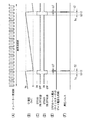
図3は、図2に示す点灯装置52の動作を説明するための波形図であり、点灯装置52の各部における概略の動作波形を模式的に示したものである。詳細には、図3(A)は、変換回路72から出力される交流電流の波形を示す図であり、図3(B)は、トランジスターQ701のベース電流の波形を示す図である。また、図3(C)は、コンデンサーC1に蓄積される電荷量を示す図である。図3(D)は、二次巻線7012から出力される高電圧パルスの波形を示す図である。
(High voltage pulse application timing)
FIG. 3 is a waveform diagram for explaining the operation of the
ここで、変換回路72の低周波駆動時(期間T1)及び高周波駆動時(期間T2)と、高電圧パルスの生成とについて説明する。
時刻t0において変換回路72が低周波駆動されると、図3(A)における「低周波期間T1」に示すように、低周波期間T1においては変換回路72により低周波の交流電流が発生する。この交流電流の周波数は導通周波数より低く、当該交流電流はハイパスフィルター740を導通しないため、当該期間T1では、図3(B)に示すように、トランジスターQ701にはベース電流が流れない。従って、低周波期間T1においては、トランジスターQ702がOFF(非導通状態)となり、サイリスターX1にゲート電圧が印加されない。このため、低周波期間T1においてはサイリスターX1のOFF状態が維持され、図3(C)に示すように、コンデンサーC1に次第に電荷が蓄積され、コンデンサーC1の電圧(Vc1)も次第に上昇する。
Here, the low-frequency driving (period T1) and high-frequency driving (period T2) of the
When the
そして、時刻t1において、変換回路72が高周波駆動されると、図3(A)における「高周波期間T2」に示すように、当該変換回路72により高周波の交流電流が発生する。この交流電流の周波数は導通周波数より高く、当該交流電流はハイパスフィルター740を導通するため、当該期間T2では、図3(B)に示すように、トランジスターQ701にベース電流が流れる。このため、時刻t1において高周波期間T2に移行し、高周波電流(第1周波数の交流電流)の波形が立ち上がると(変換回路72内のインバーターブリッジの極性が反転すると)、このタイミングで、トランジスターQ701及びQ702がONになり、サイリスターX1がON(導通)になる。サイリスターX1がONになることにより、コンデンサーC1から電荷が放出され、コンデンサーC1から一次巻線7011に電流が出力される。このため、図3(C)に示すように、時刻t1においてコンデンサーC1の放電が開始され、コンデンサーC1の電圧は0となる(より正確には、放電に必要な時間だけ遅れて0になる)。
When the
コンデンサーC1から一次巻線7011に電流が入力されると、二次巻線7012を導通する電流が昇圧され、図3(D)に示すように、時刻t1において高電圧パルスが発生する。この高電圧パルスは、ランプコネクターLCを介して電極Eに印加される。その後、時刻t2において、変換回路72が再び低周波駆動されると、図3(C)に示すように、コンデンサーC1に再び電荷の蓄積が開始される。
When a current is input from the capacitor C1 to the primary winding 7011, the current passing through the secondary winding 7012 is boosted, and a high voltage pulse is generated at time t1, as shown in FIG. 3D. This high voltage pulse is applied to the electrode E via the lamp connector LC. After that, when the
このように、点灯装置52では、放電灯511の点灯に際して、変換回路72を低周波駆動させてコンデンサーC1を充電する場合と、変換回路72を高周波駆動させて高電圧パルスの発生及び印加を行う場合と、を切り替えることができる。そして、変換回路72の低周波期間T1は、高電圧パルスの発生に伴うノイズの発生もないので、この期間内に点灯装置52の駆動状態に関する情報(例えば、降圧回路71の出力電流及び出力電圧)を取得することで、正しい情報を確実に取得できる。また、低周波期間T1において、コンデンサーC1に、二次巻線7012に供給する電荷を蓄積させることができる。このほか、当該低周波期間T1を設けることで、二次巻線7012及びコンデンサーC732,C733によって生じる自由振動を収束させる期間を設けることができ、サイリスターX1を確実に非導通状態(OFF)とすることができる。これにより、二次巻線7012で生じた高電圧が、一次巻線7011及びサイリスターX1を介して、トリガー回路74の回路素子に悪影響を及ぼすことを防止できる。このため、低周波期間T1での変換回路72の駆動周波数は、サイリスターX1が完全な非導通状態(OFF状態)となるのに十分な期間であることが望まれる。
Thus, in the
なお、コンデンサーC1への充電が開始されてから電荷を放出するまでの期間T1(時刻t0〜時刻t1)は、コンデンサーC1の静電容量及び充電時定数により予め算出することが可能である。従って、変換回路72を低周波駆動にしてコンデンサーC1への充電を開始したタイミング(時刻t0)から後、変換回路72における低周波駆動の経過時間を計測し、期間T1の経過後のタイミング(時刻t1)において変換回路72の駆動周波数を低周波駆動から高周波駆動に切り替えることにより、当該高周波駆動に切り替えるタイミングにおいて高電圧パルスを電極Eに印加することができる。
なお、コンデンサーC1への充電が完了した後、直ちに変換回路72を高周波駆動して高電圧パルスを発生させる必要はなく、コンデンサーC1への充電完後において、所望のタイミングで変換回路72を高周波駆動して高電圧パルスを発生させることもできる。
Note that the period T1 (time t0 to time t1) from the start of charging of the capacitor C1 to the release of charge can be calculated in advance from the capacitance of the capacitor C1 and the charging time constant. Accordingly, the elapsed time of the low frequency drive in the
In addition, it is not necessary to drive the
(制御部6の構成)
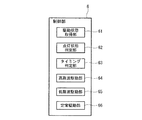
図4は、制御部6の構成を示すブロック図である。
制御部6は、前述のように、駆動回路部7の駆動を制御し、ひいては、放電灯511の点灯を制御する。具体的に、制御部6は、降圧回路71から入力される電圧及び電流に基づいて放電灯511の点灯状態を判定し、当該点灯状態に基づいて、変換回路72にゲート電圧を印加して駆動回路部7を駆動させる。
(Configuration of control unit 6)
FIG. 4 is a block diagram illustrating a configuration of the
As described above, the
このような制御部6は、図4に示すように、駆動状態取得部61、点灯状態判定部62、タイミング判定部63、高周波駆動部64、低周波駆動部65及び定常駆動部66を有する。
駆動状態取得部61は、駆動回路部7の駆動状態を示す情報(駆動状態情報)として、降圧回路71からの出力電流の電流値及び電圧値を取得する。点灯状態判定部62は、駆動状態取得部61により取得された各値に基づいて、放電灯511が点灯しているか否かを判定する。
タイミング判定部63は、点灯状態判定部62により、放電灯511が点灯していないと判定された場合に、変換回路72における低周波駆動の経過時間を計測し、変換回路72を低周波駆動から高周波駆動に切り替えるタイミング(高周波駆動タイミング)を判定する。この高周波駆動タイミングは、コンデンサーC1への充電が開始された後、コンデンサー充電期間(低周波期間T1)が経過したタイミングである。
As shown in FIG. 4, the
The drive
When the lighting
高周波駆動部64は、タイミング判定部63により高周波駆動タイミングに達したと判定された場合に、変換回路72のMOSFET721〜724に制御信号であるゲート電圧を印加して、変換回路72を高周波駆動させる。この際の変換回路72の駆動周波数(本発明の第1周波数に相当)は、前述のように、ハイパスフィルター740の導通周波数を超える周波数に設定され、当該駆動周波数は、本実施形態では50kHzに設定されている。
When the
低周波駆動部65は、タイミング判定部63により高周波駆動タイミングに達していないと判定された場合に、同様に制御信号であるゲート電圧を印加して、変換回路72を低周波駆動させる。この際の変換回路72の駆動周波数(本発明の第2周波数に相当)は、ハイパスフィルター740の導通周波数より低い周波数に設定され、当該駆動周波数は、本実施形態では500Hzに設定されている。
When the
定常駆動部66は、点灯状態判定部62により、放電灯511が点灯したと判定された場合に、同様にゲート電圧を印加して、変換回路72を更に低周波駆動させる。この際の変換回路72の駆動周波数は、本実施形態では200Hzに設定されている。
なお、この放電灯511が点灯している状態(定常点灯状態)では、パルス生成回路73の駆動は停止され、電極Eに高電圧パルスが印加されることはない。
When the lighting
In the state where the
(点灯制御処理)
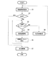
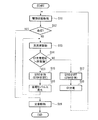
図5は、点灯装置52による放電灯511の点灯制御処理を示すフローチャートである。点灯装置52は、前述の制御ユニット93から放電灯511を点灯させる制御信号が入力されると、以下に示す点灯制御処理を実行する。この点灯制御処理は、図示しない記憶部に記憶された点灯制御プログラムに沿って行われる。
(Lighting control processing)
FIG. 5 is a flowchart showing a lighting control process of the
この点灯制御処理では、図5に示すように、まず、制御部6の駆動状態取得部61が、前述の駆動状態情報を取得する(ステップS1)。この後、点灯状態判定部62が、当該駆動状態情報に基づいて、放電灯511が点灯しているか否かを判定する(ステップS2)。ここで、点灯状態判定部62により、放電灯511が点灯していないと判定されると(ステップS2:NO)、タイミング判定部63が、前述の高周波駆動タイミングに達したか否かを判定する(ステップS3)。
In this lighting control process, as shown in FIG. 5, first, the driving
このステップS3での判定にて、タイミング判定部63により、高周波駆動タイミングに達したと判定されると(ステップS3:YES)、高周波駆動部64が、変換回路72を高周波駆動させる(ステップS4)。このため、当該変換回路72から高周波の交流電流が出力され、当該交流電流は、トリガー回路74のハイパスフィルター740を導通して、トランジスターQ701及びQ702をON(導通状態)にし、さらにサイリスターX1がON(導通状態)になる。これにより、コンデンサーC1からの出力電流が、当該サイリスターX1を介して一次巻線7011に供給され、二次巻線7012から電極Eに高電圧パルスが印加される(ステップS5)。
If it is determined by the
この後、点灯装置52は、処理をステップS3に戻し、再度、タイミング判定部63による高周波駆動タイミングの判定を行う。
そして、ステップS3での判定にて、タイミング判定部63により、高周波駆動タイミングに達していないと判定されると(ステップS3:NO)、低周波駆動部65が、変換回路72を低周波駆動させる(ステップS6)。これにより、変換回路72から出力される低周波の交流電流は、ハイパスフィルター740を導通させず、サイリスターX1における電流の導通が停止されるとともに、コンデンサーC1への蓄電が開始される。
Thereafter, the
When the
なお、変換回路72の低周波駆動時においてサイリスターX1がOFF(非導通)になることにより、コンデンサーC732,C733により自由振動が生じて昇圧された交流電流が、一次巻線7011を介して、サイリスターX1を逆流することが防止され、トリガー回路74が保護される利点がある。更に、変換回路72の低周波駆動時には、一次巻線7011への電流の供給が行われないため、前述のように、パルス生成回路73での高電圧パルスの発生に伴うノイズが発生しない。このため、制御部6は、当該低周波駆動時に処理をステップS1に戻し、駆動状態取得部61が、前述の駆動状態情報を取得する。これにより、ノイズの影響を受けていない駆動状態情報を確実に取得することができる。
Note that when the
一方、ステップS2での判定にて、点灯状態判定部62により、放電灯511が点灯したと判定されると(ステップS2:YES)、定常駆動部66が、変換回路72を低周波駆動時よりも更に低い周波数で駆動させ、駆動回路部7を定常駆動させる(ステップS7)。これにより、放電灯511が定常点灯状態に達する。
以上により、点灯制御処理が終了する。
On the other hand, if it is determined in step S2 that the
Thus, the lighting control process ends.
以上説明した本実施形態に係る点灯装置52によれば、以下の効果がある。
駆動回路部7においては、変換回路72を低周波駆動することにより、コンデンサーC1に電荷が蓄積される。このコンデンサーC1の電荷は変換回路72を高周波駆動に替えることにより一次巻線7011を通して放出され、これにより二次巻線7012にて高電圧パルスが発生する。このコンデンサーC1への充電が開始されてから電荷を放出するまでの期間T1(低周波期間T1)は、コンデンサーC1の静電容量及び充電時定数により予め算出することが可能である。従って、変換回路72を低周波駆動にしてコンデンサーC1への充電を開始した後、期間T1の経過後のタイミングにおいて変換回路72の駆動周波数を低周波駆動から高周波駆動に切り替えることにより、当該高周波駆動に切り替えるタイミングにおいて高電圧パルスを電極Eに印加することができる。
このような構成により、制御部6とパルス生成回路73とを制御線により接続して、当該制御部6が高電圧パルスを電極Eに印加させる制御信号を出力する構成に比べて、制御部6及び駆動回路部7の耐高電圧対策の構成を簡略化できる。従って、簡易な構成により放電灯511に対する高電圧パルスの印加タイミングを設定できる。
The
In the drive circuit unit 7, charges are accumulated in the capacitor C <b> 1 by driving the
With this configuration, the
また、コンデンサーC1から一次巻線7011への電流の導通状態を制御するスイッチング素子が、トランジスターQ701,Q702及びサイリスターX1で構成されている。これによれば、変換回路72の駆動周波数を低周波駆動から高周波駆動に切り替えることにより、当該トランジスターQ701,Q702が速やかに導通状態となり、ひいては、サイリスターX1が導通状態となるので、一次巻線7011に電流を速やかに供給できる。従って、変換回路72の駆動周波数を低周波駆動から高周波駆動に切り替えた後、高電圧パルスの発生までの期間を短縮することができる。
In addition, a switching element that controls a conduction state of current from the capacitor C1 to the primary winding 7011 includes transistors Q701 and Q702 and a thyristor X1. According to this, by switching the drive frequency of the
また、サイリスターX1は、大電流(電流値が大きな電流)を導通させることができるので、コンデンサーC1の静電容量が大きくても、確実に当該電流を導通させることができる。また、制御部6が、導通周波数以上の駆動周波数に応じた変換回路72の駆動と、導通周波数未満の駆動周波数に応じた変換回路72の駆動とを、高電圧パルスの印加タイミング(高周波駆動タイミング)に基づいて切り替えることで、任意のタイミングで、電極Eに高電圧パルスを印加することができる。このような制御部6による変換回路72の駆動周波数の変更は、各MOSFET721〜724にゲート電圧を印加する周波数を変更することにより行うことができるので、当該制御部6の構成を比較的簡易な構成とすることができる。従って、簡易な構成で高電圧パルスの印加タイミングを確実に設定できる。
Further, since the thyristor X1 can conduct a large current (a current having a large current value), the current can be reliably conducted even if the capacitance of the capacitor C1 is large. In addition, the
[本願出願人の先願との比較]
なお、本願出願人は、本願発明と類似した構成の点灯装置として、図11に示す構成の点灯装置について先に特許出願を行っている(特願2010−068296号)。図11に示す先願に係わる点灯装置52は、図2に示す点灯装置52と比較して、図2に示す駆動回路部7内の電流出力部750を図11に示す電流出力部750Aに変更した点が異なるものであり、他の構成は、図2に示す点灯装置52と同様である。この図11に示す電流出力部750Aについて、その概要を簡単に説明する(詳細については、特願2010−068296号を参照)。
[Comparison with the applicant's previous application]
The applicant of the present application has previously filed a patent application for a lighting device having the configuration shown in FIG. 11 as a lighting device having a configuration similar to that of the present invention (Japanese Patent Application No. 2010-068296). 11 is changed from the
図11に示す駆動回路部7内の電流出力部750Aは、ダイオードD751、抵抗R755〜R758、コンデンサーC752、ダイアックX2及びサイリスターX1を有する。このうち、コンデンサーC752は、抵抗R756とともに、ダイオードD751及び抵抗R755に対して並列に接続され、これらを介してハイパスフィルター740から入力される交流電流をダイオードD751を通して整流し、コンデンサーC752に電荷を蓄積する。
A
ダイアックX2及びサイリスターX1は第3スイッチング素子を構成し、コンデンサーC752から入力される電圧が閾値(ダイアックX2のブレイクダウン電圧)以上であると、ダイアックX2及びサイリスターX1はON(導通)し、コンデンサーC1から一次巻線7011に電流を供給する。これらのうち、ダイアックX2の入力端は、コンデンサーC752の一端に接続され、ダイアックX2の出力端は、抵抗R757を介してサイリスターX1のゲート端子に接続される。 The diac X2 and the thyristor X1 constitute a third switching element. When the voltage input from the capacitor C752 is equal to or higher than a threshold value (breakdown voltage of the diac X2), the diac X2 and the thyristor X1 are turned on (conductive), and the capacitor C1 To supply current to the primary winding 7011. Among these, the input end of the diac X2 is connected to one end of the capacitor C752, and the output end of the diac X2 is connected to the gate terminal of the thyristor X1 via the resistor R757.
そして、変換回路72が高周波駆動されると、ハイパスフィルター740から出力される高周波電流(第1周波数の交流電流)により、ダイオードD751を介して、コンデンサーC752の充電電圧が上昇する。このコンデンサーC752の電圧は、ダイアックX2に入力される。ダイアックX2は、入力される電圧(コンデンサーC752の電圧)が当該ダイアックX2に設定された閾値(ダイアックX2のブレイクダウン電圧)以上になるとONになり、コンデンサーC752からの電流を導通させて、ゲート電流としてサイリスターX1に供給する。これにより、サイリスターX1が導通し、コンデンサーC1に蓄積された電荷が一次巻線7011を通して放電され、一次巻線7011に電流が入力されることにより、二次巻線7012側に高電圧パルスが発生する。
When the
このように、図11に示す電流出力部750Aの回路構成ではダイアックX2を搭載しており、ダイアックX2の前段のコンデンサーC752の電圧がダイアックX2のブレイクダウン電圧に達するとダイアックX2がONし、これにより、サイリスターX1がONして高電圧パルスが発生する。
しかしながら、このダイアックX2は一般的な部品ではないため供給メーカーも少なく、コスト的にも割高である。また、ダイアックX2には電流増幅機能がないため、コンデンサーC752にあらかじめエネルギーを蓄えておく必要がある。よって、コンデンサーC752を充電するための時定数が必要になり、変換回路72の駆動周波数を例えば50kHzとすると、コンデンサーC752の充電時定数がこれよりも大きいため、変換回路72の高周波駆動の際に、どのタイミングで高電圧パルスを出力するかを制御できない。
As described above, the circuit configuration of the
However, since this diac X2 is not a general part, there are few suppliers and it is expensive. Further, since the diac X2 does not have a current amplification function, it is necessary to store energy in the capacitor C752 in advance. Therefore, a time constant for charging the capacitor C752 is required. When the drive frequency of the
これに対して、図2に示す点灯装置52では、入手性やコスト面で課題の多いダイアックを使用しない回路構成である。また、ダイアックの代わりに増幅機能のあるトランジスターを使用することにより、ハイパスフィルター740の電流が小さくなり、部品の信頼性、小型化に対して有利となる。また、トリガー用のエネルギー充電コンデンサーC752を使用しないため、高電圧パルス発生のタイミングは高周波電流(第1周波数の交流電流)の立ち上がり(変換回路72内のインバーターブリッジ回路の極性反転)直後で一定となり、高電圧パルス発生のタイミングを限定することができる。
On the other hand, the
[第2の実施形態]
前述した第1の実施形態の点灯装置52においては、変換回路72を低周波駆動することにより、コンデンサーC1に電荷を蓄積し、その後、変換回路72を高周波駆動に替えることによりコンデンサーC1に蓄積された電荷を一次巻線7011を通して放電するように構成されている。なお、低周波駆動とは、前述のようにハイパスフィルター740の導通周波数未満の第2周波数による駆動であり、高周波駆動とは、ハイパスフィルター740の導通周波数以上の第1周波数による駆動である。
このように、第1の実施形態では、放電灯511の点灯始動時において、変換回路72における駆動周波数を、低周波駆動と高周波駆動とに切り替える必要があり、制御部6における制御がやや複雑になる。このため、本発明の第2の実施形態として、放電灯511の点灯始動時において、変換回路72を第1周波数による高周波駆動のみとする例について説明する。
[Second Embodiment]
In the
Thus, in the first embodiment, at the start of lighting of the
図6は、本発明の第2の実施形態に係わる点灯装置52の構成を示す図である。図6に示す点灯装置52は、図2に示す点灯装置52と比較して、駆動回路部7内に電圧監視回路760を新たに追加した点が異なり、他の構成は、図2に示す点灯装置52と同様である。このため、同一の構成部分には同一の符号を付し、重複する説明は省略する。
FIG. 6 is a diagram showing a configuration of a
図6に示す電圧監視回路760は、ツェナーダイオードZD701と、NPN型のバイポーラトランジスターQ703と、NPN型のバイポーラトランジスターQ704とを備えて構成される。この電圧監視回路760は、コンデンサーC1の充電電圧を監視するとともに、コンデンサーC1の充電電位が所定の電圧値より低い場合に、ハイパスフィルター740から出力される高周波電流(第1周波数の交流電流)を電流出力部750に流さないようにする。また、電圧監視回路760は、コンデンサーC1の充電電位が所定の電圧値以上の場合に、ハイパスフィルター740から出力される高周波電流を電流出力部750に流し、トランジスターQ701,Q702及びサイリスターX1をON(導通)にする。
The
この図6に示す電圧監視回路760において、コンデンサーC1の両端に、抵抗R761と、抵抗R762と、抵抗R763とがこの順に直列接続される。この直列回路においては、抵抗R761の一端がコンデンサーC1の一端(ノードN11)に接続され、抵抗R761の他端は抵抗R762の一端に接続され、抵抗R762の他端は抵抗R763の一端に接続され、抵抗R763の他端は、コンデンサーC1に他端に接続される。すなわち、抵抗R763の他端は、MOSFET722,724の各ソース(変換回路72の負(−)側の出力端子)に接続される。
In the
また、抵抗R762と抵抗R763との接続点(ノードN13)とトランジスターQ703のベース端子との間にはツェナーダイオードZD701が接続され、このツェナーダイオードZD701のカソード端子がノードN13に接続され、アノード端子がトランジスターQ703のベース端子に接続される。トランジスターQ703のエミッター端子は、MOSFET722及び724の各ソースに接続され、トランジスターQ703のコレクター端子は、抵抗R764を介して制御回路電源Vccに接続される。また、トランジスターQ703のコレクター端子には、トランジスターQ704のベース端子が接続され、このトランジスターQ704のコレクター端子は、ハイパスフィルター740内の抵抗R742とR743の接続点(ノードN12)に接続されている。
A Zener diode ZD701 is connected between the connection point (node N13) between the resistor R762 and the resistor R763 and the base terminal of the transistor Q703, the cathode terminal of the Zener diode ZD701 is connected to the node N13, and the anode terminal is Connected to the base terminal of transistor Q703. The emitter terminal of the transistor Q703 is connected to the sources of the
上記構成において、コンデンサーC1の充電電圧(ノードN11の電圧)が上昇するに従い、抵抗R762と抵抗R763との接続点(ノードN13)の電圧も次第に上昇する。そして、ノードN13の電圧が、ツェナーダイオードZD701のツェナー降伏電圧(より正確には、ツェナー降伏電圧とトランジスターQ703のVBE(ベース・エミッター間電圧)とを加算した電圧)より低い場合は、ツェナーダイオードZD701が非導通であり、トランジスターQ703にベース電流が流れない。このため、トランジスターQ703はOFFとなり、トランジスターQ704のベースには、電源Vccから抵抗R764を通して電流が流れ、トランジスターQ704はONになる。このため、ノードN12の電位は0(より正確には、トランジスターQ704のVCE(コレクター・エミッター間の飽和電圧))となる。 In the above configuration, as the charging voltage of the capacitor C1 (the voltage at the node N11) increases, the voltage at the connection point (node N13) between the resistor R762 and the resistor R763 also gradually increases. When the voltage at the node N13 is lower than the Zener breakdown voltage of the Zener diode ZD701 (more precisely, the voltage obtained by adding the Zener breakdown voltage and the VBE (base-emitter voltage) of the transistor Q703), the Zener diode ZD701. Is non-conductive, and the base current does not flow through the transistor Q703. For this reason, the transistor Q703 is turned off, a current flows from the power source Vcc through the resistor R764 to the base of the transistor Q704, and the transistor Q704 is turned on. For this reason, the potential of the node N12 becomes 0 (more precisely, the VCE of the transistor Q704 (the saturation voltage between the collector and the emitter)).
このため、ノードN13の電圧が、ツェナーダイオードZD701のツェナー降伏電圧より低い場合は、ハイパスフィルター740から出力される高周波電流はトランジスターQ704によりバイパスされる。このため、電流出力部750には、ハイパスフィルター740から高周波電流が流れず、サイリスターX1は非導通の状態を維持する。
For this reason, when the voltage at the node N13 is lower than the Zener breakdown voltage of the Zener diode ZD701, the high-frequency current output from the high-
一方、コンデンサーC1の充電電圧がさらに上昇し、ノードN13の電圧が、ツェナーダイオードZD701のツェナー降伏電圧以上になると、ツェナーダイオードZD701が導通となり、トランジスターQ703にベース電流が流れようになる。このため、トランジスターQ703はONとなり、トランジスターQ704のベースには電流が流れず、トランジスターQ704はOFFになる。 On the other hand, when the charging voltage of the capacitor C1 further rises and the voltage at the node N13 becomes equal to or higher than the Zener breakdown voltage of the Zener diode ZD701, the Zener diode ZD701 becomes conductive, and the base current flows through the transistor Q703. Therefore, the transistor Q703 is turned on, no current flows through the base of the transistor Q704, and the transistor Q704 is turned off.
このため、ノードN13の電圧が、ツェナーダイオードZD701のツェナー降伏電圧以上の場合は、ハイパスフィルター740から出力される高周波電流が、電流出力部750内のトランジスターQ701のベース端子に流れるようになる。これによりトランジスターQ701及びQ702がONとなり、サイリスターX1のゲートに抵抗R753を介して電源Vccからゲート電流が流れる。このため、サイリスターX1は導通となり、コンデンサーC1に充電された電荷が一次巻線7011を通して放電され、トランスT701の一次巻線7011に電流が流れることにより、トランスT701の二次巻線7012側に高電圧パルスが発生する。
このように、第2の実施形態では、放電灯511の点灯始動時において、変換回路72を常に高周波駆動(第1周波数による駆動)するとともに、コンデンサーC1の充電電圧を電圧監視回路760により監視する。そして、コンデンサーC1の充電電圧が所定の電圧値以上になった場合に、これを検出して、ハイパスフィルター740から出力される高周波電流を電流出力部750に流してサイリスターX1を導通にし、コンデンサーC1から一次巻線7011に電流を流して高電圧パルスを発生させる。
For this reason, when the voltage of the node N13 is equal to or higher than the Zener breakdown voltage of the Zener diode ZD701, the high-frequency current output from the high-
Thus, in the second embodiment, when the
図7は、図6に示す点灯装置52の動作を説明するための波形図であり、点灯装置52の各部における概略の動作波形を模式的に示したものである。詳細には、図7(A)は、変換回路72から出力される交流電流(高周波電流)の波形を示す図であり、図7(B)は、コンデンサーC1の充電電圧(Vc1)の波形を示す図である。また、図7(C)は、電圧監視回路760内のトランジスターQ703のON/OFF状態を示す図であり、図7(D)は、同じく電圧監視回路760内のトランジスターQ704のON/OFF状態を示す図である。図7(E)は、トランジスターQ701のベース電流の波形を示す図であり、図7(F)は、二次巻線7012から出力される高電圧パルスの波形を示す図である。
FIG. 7 is a waveform diagram for explaining the operation of the
図7(A)に示すように、放電灯511の点灯始動時には、変換回路72は常に高周波駆動される。すなわち、ハイパスフィルター740にはコンデンサーC741を通して、常に高周波電流が流れている。
上記変換回路72の高周波駆動の状態において、時刻t0以前、すなわち、図7(B)に示すコンデンサーC1の電圧が所定の電圧値Vaより低い場合には(ノードN13の電圧が、ツェナーダイオードZD701のツェナー降伏電圧より低い場合には)、前述しツェナーダイオードZD701の作用により、図7(C)に示すようにトランジスターQ703はOFFとなり、また図7(D)に示すように、トランジスターQ704はONになる。このため、ハイパスフィルター740内のノードN12の電位は0となり、ハイパスフィルター740から出力される高周波電流はトランジスターQ704によりバイパスされる。このため、図7(E)に示すように、電流出力部750には、ハイパスフィルター740から電流が流れず、また、図7(F)に示すように、サイリスターX1は非導通の状態を維持し、トランスT701には高圧パルスが流れない。
As shown in FIG. 7A, the
In the high frequency driving state of the
その後、コンデンサーC1の充電電圧がさらに上昇し、図7(B)に示すように、時刻t1において、コンデンサーC1の電圧が所定の電圧値よりも以上になると(ノードN13の電圧が、ツェナーダイオードZD701のツェナー降伏電圧よりも以上になると)、図7(C)及び(D)に示すように、トランジスターQ703はONとなり、トランジスターQ704はOFFになる。これにより、時刻t1以降は、ハイパスフィルター740から出力される高周波電流(第1周波数の交流電流)を電流出力部750に流すことが可能になる。
Thereafter, the charging voltage of the capacitor C1 further rises, and as shown in FIG. 7B, when the voltage of the capacitor C1 exceeds a predetermined voltage value at time t1 (the voltage at the node N13 becomes the zener diode ZD701). As shown in FIGS. 7C and 7D, the transistor Q703 is turned on and the transistor Q704 is turned off. Thus, after time t1, it is possible to flow a high-frequency current (a first-frequency alternating current) output from the high-
そして時刻t1において、変換回路72から出力される高周波電流の波形が立ち上がると(変換回路72内のインバーターブリッジの極性が反転すると)、図7(E)に示すように、時刻t1においてトランジスターQ701にベース電流が流れ始める。トランジスターQ701にベース電流が流れることにより、サイリスターX1がON(導通)となる。時刻t1において、サイリスターX1がONすることにより、図7(B)に示すように、コンデンサーC1の電荷がトランスT701の一次巻線7011を通して放電され、コンデンサーC1が0となる(より正確には、放電に必要な時間だけ遅れて0になる)。
When the waveform of the high-frequency current output from the
時刻t1において、サイリスターX1がONし、一次巻線7011に電流が流れると、図7(F)に示すように、時刻t1において二次巻線7012に高電圧パルスが発生する。この高電圧パルスは、ランプコネクターLCを介して電極Eに印加される。 When the thyristor X1 is turned on at time t1 and a current flows through the primary winding 7011, a high voltage pulse is generated in the secondary winding 7012 at time t1, as shown in FIG. 7F. This high voltage pulse is applied to the electrode E via the lamp connector LC.
そして、図7(B)に示すように、コンデンサーC1の電荷がトランスT701の一次巻線7011を通して放電されることにより、コンデンサーC1の充電電圧が低下する。このコンデンサーC1の充電電圧が低下することにより、図7(C)及び(D)に示すように、時刻t2において、電圧監視回路760内のトランジスターQ703はOFFとなり、トランジスターQ704はONになる。なお、時刻t2は、コンデンサーC1の電圧が所定の電圧値Vaより低くなる時刻であるが、この図では、図面の見易さのために、時間を長く伸ばした形で示している。
Then, as shown in FIG. 7B, the charge of the capacitor C1 is lowered by discharging the charge of the capacitor C1 through the primary winding 7011 of the transformer T701. As the charging voltage of the capacitor C1 decreases, as shown in FIGS. 7C and 7D, the transistor Q703 in the
これにより、時刻t2以降、トランジスターQ701に流れるベース電流(ハイパスフィルター740から出力される高周波電流)が遮断される(トランジスターQ704により高周波電流がバイパスされる)。その後、コンデンサーC1の放電が完了し、サイリスターX1が非導通となると、コンデンサーC1への充電が再び開始される。 Thereby, the base current (high-frequency current output from the high-pass filter 740) flowing through the transistor Q701 after time t2 is cut off (the high-frequency current is bypassed by the transistor Q704). Thereafter, when the discharge of the capacitor C1 is completed and the thyristor X1 becomes non-conductive, charging of the capacitor C1 is started again.
なお、コンデンサーC1への充電が開始されてから充電電圧が所定の電圧値Vaに到達するまでの期間は、コンデンサーC1の静電容量、充電時定数、電圧監視回路760内のツェナーダイオードZD701のツェナー降伏電圧を基に、予め算出することができる。また、時刻t0においてコンデンサーC1の充電電圧が所定の電圧Vaに到達した後、時刻t1において、変換回路72から出力される高周波電流の波形が立ち上がるまでの期間Ts(時刻t0〜t1)は、ごく短い期間(例えば、数10μsec以下)に抑えることができる。このため、コンデンサーC1への充電を開始してから放電灯511に高電圧パルスを印加するまでのタイミングを、コンデンサーC1の静電容量、充電時定数、電圧監視回路760内のツェナーダイオードZD701のツェナー降伏電圧を基に、容易かつ正確に決定することができる。
It should be noted that during the period from when charging of the capacitor C1 is started until the charging voltage reaches a predetermined voltage value Va, the capacitance of the capacitor C1, the charging time constant, the zener of the zener diode ZD701 in the
(制御部6の構成)
図8は、第2の実施形態における制御部6の構成を示すブロック図である。図8に示す制御部6は、図4に示す制御部6と比較して、図4に示す制御部6内のタイミング判定部63と低周波駆動部65を削除した点が異なり、他の構成は、図4に示す制御部6と同様である。このため、同一の構成部分には同一の符号を付し、重複する説明は省略する。
(Configuration of control unit 6)
FIG. 8 is a block diagram showing the configuration of the
すなわち、図8に示す第2の実施形態における制御部6では、変換回路72における低周波駆動と高周波駆動との切り替えのタイミングを判定する必要がなく、このためタイミング判定部63が不要になる。また、変換回路72における低周波駆動が行われないため、低周波駆動部65が不要になる。
That is, in the
(点灯制御処理)
図9は、第2の実施形態における点灯装置52による放電灯511の点灯制御処理を示すフローチャートである。点灯装置52は、前述の制御ユニット93から放電灯511を点灯させる制御信号が入力されると、以下に示す点灯制御処理を実行する。この点灯制御処理は、図示しない記憶部に記憶された点灯制御プログラムに沿って行われる。
(Lighting control processing)
FIG. 9 is a flowchart showing a lighting control process for the
この点灯制御処理では、図9に示すように、まず、制御部6の駆動状態取得部61が、前述の駆動状態情報を取得する(ステップS11)。この後、点灯状態判定部62が、当該駆動状態情報に基づいて、放電灯511が点灯しているか否かを判定する(ステップS12)。ここで、点灯状態判定部62により、放電灯511が点灯していないと判定されると(ステップS12:NO)、高周波駆動部64が、変換回路72を高周波駆動させる(ステップS13)。このため、当該変換回路72から高周波電流(第1周波数の交流電流)が出力される。
In this lighting control process, as shown in FIG. 9, first, the drive
その後、電圧監視回路760によりコンデンサーC1の充電電圧が所定の電圧値Vaと比較される(ステップS14)。そして、コンデンサーC1の電圧が所定の電圧値Va以上の場合は(ステップS14:YES)、電圧監視回路760内のトランジスターQ703はONとなり、またトランジスターQ704はOFFになる(ステップS15)。
この状態において、変換回路72から出力される高周波電流が立ち上がると(変換回路72内のインバーターブリッジの極性が反転すると)、電流出力部750内のトランジスターQ701にベース電流が流れ始める。トランジスターQ701にベース電流が流れることにより、トランジスターQ701及びQ702がONになり、サイリスターX1が導通となり、コンデンサーC1の電荷がトランスT701の一次巻線7011を通して放電され、一次巻線7011に電流が流れる。一次巻線7011に電流が入力されると、二次巻線7012を導通する電流が昇圧され高電圧パルスが発生する。この高電圧パルスは、ランプコネクターLCを介して電極Eに印加される(ステップS16)。
Thereafter, the
In this state, when the high-frequency current output from the
ステップS16において、コンデンサーC1の電荷がトランスT701の一次巻線7011を通して放電されることにより、コンデンサーC1の充電電圧が低下する。このコンデンサーC1の充電電圧が低下すると、電圧監視回路760内のトランジスターQ703はOFFとなり、トランジスターQ704はONになる。これにより、電流出力部750内のトランジスターQ701のベース電流が遮断される。そして、コンデンサーC1の放電が完了するとサイリスターX1が非導通となり、この後、ステップS13に戻る。
In step S16, the electric charge of the capacitor C1 is discharged through the primary winding 7011 of the transformer T701, so that the charging voltage of the capacitor C1 decreases. When the charging voltage of the capacitor C1 is lowered, the transistor Q703 in the
一方、ステップS14において、コンデンサーC1の電圧が所定の電圧値Vaより低いと判定された場合は(ステップS14:NO)、電圧監視回路760内のトランジスターQ703はOFFとなり、またトランジスターQ704はONになる(ステップS17)。これにより、ハイパスフィルター740内のノードN12の電位は0となり、ハイパスフィルター740から出力される高周波電流はトランジスターQ704によりバイパスされる。このため、電流出力部750には、ハイパスフィルター740から電流が流れず、サイリスターX1は非導通の状態を維持する。そして、コンデンサーC1の充電の開始、あるいは、コンデンサーC1への充電を継続するとともに(ステップS18)、その後、ステップS11に戻る。
On the other hand, when it is determined in step S14 that the voltage of the capacitor C1 is lower than the predetermined voltage value Va (step S14: NO), the transistor Q703 in the
一方、ステップS12での判定にて、点灯状態判定部62により、放電灯511が点灯したと判定された場合は(ステップS12:YES)、定常駆動部66が、変換回路72を低周波駆動時よりも更に低い周波数で駆動させ、駆動回路部7を定常駆動させる(ステップS19)。これにより、放電灯511が定常点灯状態に達する。
以上により、点灯制御処理が終了する。
On the other hand, when it is determined in step S12 that the
Thus, the lighting control process ends.
以上説明したように、本発明の第2の実施形態では、放電灯511の点灯始動時において、変換回路72を常に第1周波数で高周波駆動しておくとともに、コンデンサーC1の充電電圧を電圧監視回路760により監視する。そして、コンデンサーC1の充電電圧が所定の電圧値Va以上になったことを検出して、ハイパスフィルター740から入力される高周波電流を電流出力部750に流し、トランジスターQ701,Q702及びサイリスターX1をON(導通)にし、コンデンサーC1に蓄積された電荷を放電して一次巻線7011に電流を流し、高電圧パルスを放電灯511の電極に印加する。
これにより、放電灯511の点灯始動時に変換回路72における駆動周波数の切り替えの必要がなくなる。また、高電圧パルスの発生のタイミングを電圧監視回路760により自動で検出して制御できるとともに、コンデンサーC1の充電開始から高電圧パルスの発生までの期間を短縮することができる。また、制御部6の構成をより簡略化できる。
As described above, in the second embodiment of the present invention, at the start of lighting of the
This eliminates the need to switch the driving frequency in the
なお、第2の実施形態では、コンデンサーC1の充電電圧の監視のために、トリガー回路74内に電圧監視回路760を設けた例について説明したが、制御部6においてコンデンサーC1の電圧を監視するようにしてもよい。この場合は、電圧監視回路760内のトランジスターQ704を制御部6からの信号により直接にON/OFF制御する。例えば、コンデンサーC1の充電電圧が所定の電圧値Vaより低い場合は、トランジスターQ704をONにして、ハイパスフィルター740から出力される高周波電流を電流出力部750に流さないようにし、コンデンサーC1の充電電圧が所定の電圧値Va以上になった場合に、トランジスターQ704をOFFにして、ハイパスフィルター740から出力される高周波電流を電流出力部750に流すようにする。
In the second embodiment, the example in which the
[第2の実施形態の変形例]
前述した第2の実施形態では、放電灯511の点灯始動時に低周波期間がない場合(換言すると、変換回路72が高周波数で駆動され続ける場合)の例であり、また、駆動回路部7内に電圧監視回路760を設けた例である。従って、変換回路72が高周波数で駆動され続けることにより、変換回路72で生じた高周波の交流電流が、コンデンサーC741及びトランジスターQ701のベースに入力され続ける。このような高周波電流は電圧が高いため、不必要に連続して発生及び出力されると、ノイズが増大することによる対策が必要になり、また点灯装置52の回路構成、及び、電極Eを劣化させる要因となる。
[Modification of Second Embodiment]
The second embodiment described above is an example in the case where there is no low frequency period when the
このため、図10に示すように、第2の実施形態を変形して、第1の実施形態と同様に、変換回路72の低周波期間T1を設けることができる。図10に示す例では、前回の高周波期間T2の終了時(時刻t3)から、次に高周波駆動を開始する時刻t1までの期間において、変換回路72を低周波駆動させることで高周波電流が発生しない期間を設けている。
For this reason, as shown in FIG. 10, the second embodiment can be modified to provide a low frequency period T <b> 1 of the
なお、図10に示す第2の実施形態の変形例では、変換回路72における低周波駆動と高周波駆動を切り替える必要があるため、制御部6については、図4に示す制御部6と同様な構成となり、タイミング判定部63により低周波駆動と高周波駆動の切り替えタイミングを判定し、低周波駆動部65により変換回路72を低周波駆動し、高周波駆動部64により変換回路72を高周波駆動する。
In the modification of the second embodiment shown in FIG. 10, since it is necessary to switch between the low frequency driving and the high frequency driving in the
上述した第2の実施形態の変形例では、低周波期間T1を設けることにより、変換回路72で生じた高周波電流がハイパスフィルター740やパルス生成回路73等に不必要に入力され続けることがなくなる。また、変換回路72の低周波期間においては、高周波の交流電流の発生に伴うノイズの発生もないので、この期間内に駆動回路部7の駆動状態に関する情報(例えば、降圧回路71の出力電流及び出力電圧)を取得することで、正しい情報を確実に取得できる。
In the modification of the second embodiment described above, by providing the low frequency period T1, the high frequency current generated in the
以上、本発明の第1の実施形態、第2の実施形態、及び第2の実施形態の変形例
ついて説明した、ここで、本発明の点灯装置と上記実施形態との対応関係について補足して説明しておく。すなわち、本発明におけるプロジェクターは、上記実施形態においてプロジェクター1が対応し、本発明における点灯装置は、制御部6及び駆動回路部7を備える点灯装置52が対応する。また、本発明における一対の第1スイッチング素子は、MOSFET721(S1)とMOSFET724(S4)とが対応し、また、本発明における一対の第2スイッチング素子は、MOSFET722(S2)とMOSFET723(S3)とが対応する。
As described above, the first embodiment, the second embodiment, and the modified example of the second embodiment of the present invention have been described. Here, the correspondence relationship between the lighting device of the present invention and the above embodiment is supplemented. Let me explain. That is, the projector according to the present invention corresponds to the
また、本発明における第1スイッチング素子と第2スイッチング素子の接続点である中点は、MOSFET721(S1)のソースとMOSFET722(S2)のドレインとの接続点(ノードN1)、或いは、MOSFET723(S3)のソースとMOSFET724(S4)のドレインとの接続点(ノードN2)が対応する。また、本発明における変換回路は、変換回路72が対応し、本発明におけるパルス生成回路は、パルス生成回路73が対応し、本発明におけるトリガー回路は、トリガー回路74が対応する。また、本発明におけるコンデンサーは、コンデンサーC1が対応し、本発明におけるハイパスフィルターは、ハイパスフィルター740が対応する。また、本発明における第3スイッチング素子は、第1トランジスターQ701と、第2トランジスターQ702と、サイリスターX1とが対応する。また、本発明における制御部は、制御部6が対応する。
Further, the midpoint as the connection point between the first switching element and the second switching element in the present invention is the connection point (node N1) between the source of the MOSFET 721 (S1) and the drain of the MOSFET 722 (S2), or the MOSFET 723 (S3). ) And the connection point (node N2) between the drain of MOSFET 724 (S4). The conversion circuit in the present invention corresponds to the
また、本発明における電圧監視回路は、電圧監視回路760が対応し、本発明における放電灯は、放電灯511が対応し、本発明における光変調装置は、液晶パネル442が対応し、本発明における投射光学装置は、投射光学装置3が対応する。また、本発明におけ
る所定周波数は、ハイパスフィルター740を導通にする交流電流の周波数と、ハイパスフィルター740を非導通にする交流電流の周波数とを区分する基準となる周波数(導通周波数とも呼び、例えば、20kHz)が対応する。また、本発明における所定周波数以上の周波数(第1周波数)は、導通周波数(例えば、20kHz)以上の周波数(ハイパスフィルター740に交流電流を流すことができる周波数、例えば、50kHz)が対応し、本発明における所定周波数未満の第2周波数は、導通周波数(例えば、20kHz)未満の周波数(ハイパスフィルターに交流電流を流すことができない周波数、例えば、500Hz)が対応する。また、本発明における高周波駆動は、変換回路72を第1周波数(例えば、50kHz)で駆動することが対応し、低周波駆動は、変換回路72を第2周波数(例えば、500Hz)で駆動することが対応する。
The voltage monitoring circuit according to the present invention corresponds to the
そして、上記実施形態において、本発明の点灯装置52は、放電灯511の電極Eに電力を供給して、放電灯511を点灯させる点灯装置52であって、それぞれ直流電流が入力される一対の第1スイッチング素子(MOSFET721と724)及び一対の第2スイッチング素子(MOSFET722と723)を有し、上記一対の第1スイッチング素子(MOSFET721と724)及び上記一対の第2スイッチング素子(MOSFET722と723)のうちの一方が導通状態となり他方が非導通状態となる状態変化が交互に切り替わることで、上記直流電流を交流電流に変換する変換回路72と、変換回路72から入力される交流電流から高電圧パルスを生成し、当該高電圧パルスを電極Eに印加するパルス生成回路73と、パルス生成回路73に高電圧パルスを生成させるトリガー回路74と、上記直流電流により電荷が蓄積されるコンデンサーC1と、を備え、上記パルス生成回路73は、トリガー回路74に接続される一次巻線7011と、変換回路72に接続される二次巻線7012とを備えるトランスT701を有し、一次巻線7011に入力される電流に応じて、二次巻線7012に入力される電流を昇圧して高電圧パルスを生成し、上記トリガー回路74は、第1スイッチング素子(MOSFET721)と第2スイッチング素子(MOSFET722)の接続点である中点(ノードN1)と接続され、変換回路72から上記所定周波数以上の交流電流が入力されると当該交流電流を導通させ、上記所定周波数未満の周波数の交流電流が入力されると当該交流電流を遮断するハイパスフィルター740と、ハイパスフィルター740を介して上記所定周波数以上の交流電流が入力された場合、コンデンサーC1に蓄積された電荷を放電させることにより一次巻線7011に電流を流す第3スイッチング素子と、を有する。
And in the said embodiment, the
このような構成の点灯装置52では、放電灯511の点灯始動時において、変換回路72の駆動を、所定周波数未満の周波数により低周波駆動する低周波期間T1と、所定周波数以上の周波数により高周波駆動する高周波期間T2との間で切り替えができるようにする。この変換回路72の低周波期間T1においては、ハイパスフィルター740が非導通となり第3スイッチング素子(サイリスターX1)がON(導通)しないので、この低周波期間T1においてコンデンサーC1への充電を行う。そして、低周波期間T1においてコンデンサーC1への充電が完了した後に、変換回路72を高周波駆動に切り替え、ハイパスフィルター740を導通させることにより第3スイッチング素子(サイリスターX1)をON(導通)にする。この第3スイッチング素子をON(導通)にすることにより、コンデンサーC1に蓄積された電荷をトランスT701の一次巻線7011を通して放電し、一次巻線7011に電流を流すことによりパルス生成回路73(二次巻線7012)に高電圧パルスを発生させ、この高電圧パルスを放電灯511の電極Eに印加する。
これにより、簡易な構成により放電灯511に対する高電圧パルスの印加タイミングを設定できる点灯装置52を提供することができる。
In the
Thereby, the
また、上記実施形態において、第3スイッチング素子は、ハイパスフィルター740を介して入力される交流電流により駆動される第1トランジスターQ701と、第1トランジスターQ701により駆動される第2トランジスターQ702と、第2トランジスターQ702により制御されるゲートと、コンデンサーC1の一端に一次巻線7011を介して接続されるアノードと、コンデンサーC1の他端に接続されるカソードを有するサイリスターX1と、を備え、第1トランジスターQ701がハイパスフィルター740を介して入力される交流電流により駆動された場合に、サイリスターX1が導通となりコンデンサーC1に蓄積された電荷を放電させることにより一次巻線7011に電流を流す。
In the above embodiment, the third switching element includes a first transistor Q701 driven by an alternating current input via the high-
このような構成の点灯装置52では、第3スイッチング素子が、トランジスターQ701,Q702及びサイリスターX1で構成されていることにより、変換回路72が低周波駆動から高周波駆動に切り替わった際に、速やかに応答してコンデンサーC1の電荷放出を行い、一次巻線7011に電流を供給することができる。従って、コンデンサーC1の電荷の充電完了から高電圧パルスの発生までの期間を短縮することができる。また、任意のタイミングで高電圧パルスを確実に印加できる。さらに、サイリスターX1は大電流を導通させることができるので、コンデンサーC1の静電容量が大きくても、このコンデンサーC1の放電電流を確実に導通させることができる。
In the
また、上記実施形態において、点灯装置52は、一対の第1スイッチング素子(MOSFET721及び724)及び一対の第2スイッチング素子(MOSFET722及び723)の導通状態及び非導通状態を制御する制御信号を出力して、変換回路72を駆動させる制御部6を備える。
Moreover, in the said embodiment, the
このような構成の点灯装置52では、制御部6が変換回路72に制御信号を出力することで、第1スイッチング素子(MOSFET721及び724)及び第2スイッチング素子(MOSFET722及び723)の導通状態及び非導通状態を確実に制御でき、ひいては、変換回路72を低周波(所定周波数未満の周波数)及び高周波(所定周波数以上の周波数)で駆動させることができる。従って、コンデンサーC1を充電する場合と、高電圧パルスを発生及び印加させる場合と、を適切に制御できる。
In the
また、上記実施形態において、制御部6は、パルス生成回路73により高電圧パルスを電極Eに印加するタイミングに基づいて、変換回路72の駆動周波数を、所定周波数より低い第2周波数から所定周波数以上の第1周波数に切り替える。
Moreover, in the said embodiment, the
このような構成の点灯装置52では、制御部6が、所定周波数より低い周波数(導通周波数未満の周波数)である第2周波数で変換回路72を駆動することで、変換回路72から出力される交流電流がハイパスフィルター740を導通しないようにして(第3スイッチング素子を非導通にして)、コンデンサーC1を充電する。そして、コンデンサーC1の充電が完了した後に、所定周波数以上(導通周波数以上)である第1周波数に変換回路の駆動周波数を変更することで、コンデンサーC1に蓄積された電荷を放電させて一次巻線7011に電流を流し、二次巻線7012に発生した高電圧パルスを放電灯511の電極Eに印加する。そして、制御部6が、第2周波数での変換回路72の駆動と、第1周波数での変換回路72の駆動とを、高電圧パルスの印加タイミングに基づいて切り替えることで、任意のタイミングで、電極Eに高電圧パルスを印加することができる。
In the
また、上記実施形態において、制御部6は、変換回路72の駆動周波数を第2周波数で所定の時間駆動させた後、第1周波数に切り替える。
In the above embodiment, the
このような構成の点灯装置52では、制御部6が、第2周波数で変換回路72を所定時間(低周波期間T1)駆動してコンデンサーへの充電を完了させる。その後に、変換回路72を第1周波数で駆動し、コンデンサーC1に蓄積された電荷を放電させることにより一次巻線7011に電流を流し、二次巻線7012に発生した高電圧パルスを放電灯511の電極Eに印加する。
これにより、変換回路72を第2周波数で所定時間駆動することによりコンデンサーC1を充電できる。そして、変換回路72の駆動周波数を第1周波数に変更し、コンデンサーC1に蓄積された電荷を放電させることにより一次巻線7011に電流を流し、高電圧パルスを発生させて放電灯511の電極Eに印加することができる。このため、簡易な構成で高電圧パルスの印加タイミングを確実に設定できる。
In the
Accordingly, the capacitor C1 can be charged by driving the
また、上記実施形態において、点灯装置52は、上記一対の第1スイッチング素子(721及び724)及び上記一対の第2スイッチング素子(722および723)の導通状態及び非導通状態を制御する制御信号を出力して、変換回路72を駆動させる制御部6を備え、制御部6は、放電灯511の点灯始動時に変換回路72を常に所定周波数以上の周波数で駆動させ、トリガー回路74は、第1トランジスターQ701に対して、ハイパスフィルター740を介して入力される交流電流を入力するか、または第1トランジスターQ701をオフさせる電圧を印加するか、を切り替える電圧監視回路760を備え、この電圧監視回路760は、コンデンサーC1の電圧が所定電圧Vaより低い場合、第1トランジスターQ701をオフさせる制御をし、コンデンサーC1の電圧が所定電圧Va以上の場合、ハイパスフィルター740を介して入力される交流電流を第1トランジスターQ701に入力させる制御をする。
Moreover, in the said embodiment, the
このような構成の点灯装置52では、放電灯511の点灯始動時において、制御部6が、変換回路72を常に所定周波数以上(導通周波以上)の周波数で駆動し、電圧監視回路760が、コンデンサーC1の充電電圧を監視する。そして、コンデンサーC1の充電電圧が所定の電圧値Va以上になったことを検出して、変換回路72から入力される高周波電流(所定周波数以上の交流電流)を第1トランジスターQ701に流すことにより、この第1トランジスターQ701をONにし、ひいては、サイリスターX1を導通にし、コンデンサーC1に蓄積された電荷を放電させることにより一次巻線7011に電流を流し、二次巻線7012に発生した高電圧パルスを放電灯511の電極Eに印加する。
これにより、放電灯511の点灯始動時において、変換回路72における駆動周波数の切り替えの必要がなくなる。また、高電圧パルスの発生のタイミングを電圧監視回路760により自動で検出して制御できる。このため、コンデンサーC1の充電開始から高電圧パルスの発生までの期間を短縮することができる。また、制御部6の構成をより簡略化できる。
In the
This eliminates the need to switch the driving frequency in the
また、上記実施形態において、プロジェクター1は、上記に記載の点灯装置52と、点灯装置52により供給される電力により点灯される放電灯511と、この放電灯511を有する照明装置から出射された光束を変調する光変調装置(液晶パネル442)と、変調された光束を投射する投射光学装置3と、を備える。
In the above embodiment, the
このような構成のプロジェクター1によれば、前述の点灯装置52と同様の効果を奏することができる。また、前述のように、不要な高電圧パルスの電極に対する印加を抑制できるので、放電灯511の長寿命化、ひいては、照明装置の長寿命化を図れる。更には、放電灯511の交換等のプロジェクター1のメンテナンスを簡略化できる。
According to the
以上、本発明の実施形態について説明したが、本発明は前述の実施形態に限定されるものではなく、本発明の目的を達成できる範囲での変形、改良等は本発明に含まれるものである。特に、点灯装置を構成する各回路素子の数、配置及び構成については、上記実施形態に限定されるものではない。 Although the embodiments of the present invention have been described above, the present invention is not limited to the above-described embodiments, and modifications, improvements, and the like within the scope that can achieve the object of the present invention are included in the present invention. . In particular, the number, arrangement, and configuration of each circuit element constituting the lighting device are not limited to the above embodiment.
前記実施形態では、第3スイッチング素子として、トランジスターQ701,Q702及びサイリスターX1を採用したが、本発明はこれに限らない。例えば、トランジスターQ701,Q702に代えてFETを採用することもでき、サイリスターX1に代えてパワーMOSFETを採用してもよい。すなわち、コンデンサーC1からの電荷の放出に対して、速やかに非導通状態から導通状態に変化することができ、かつ、大電流を導通可能な構成であればよい。 In the above embodiment, the transistors Q701 and Q702 and the thyristor X1 are employed as the third switching element, but the present invention is not limited to this. For example, an FET may be employed instead of the transistors Q701 and Q702, and a power MOSFET may be employed instead of the thyristor X1. That is, any structure that can quickly change from a non-conducting state to a conducting state with respect to the discharge of electric charge from the capacitor C1 and can conduct a large current may be used.
また、上記実施形態では、ハイパスフィルター740の導通周波数を20kHzとし、高周波期間及び低周波期間における変換回路72の駆動周波数をそれぞれ50kHz及び500Hzとしたが、本発明はこれに限らない。すなわち、これらの値は適宜設定可能である。
In the above embodiment, the conduction frequency of the high-
また、上記実施形態では、プロジェクター1は、3つの液晶パネル442R,442G,442Bを備えるとしたが、本発明はこれに限らない。すなわち、2つ以下、あるいは、4つ以上の液晶パネルを用いたプロジェクターにも、本発明を適用可能である。また、上記実施形態では、画像形成装置4は平面視略L字形状を有した構成を説明したが、これに限らず、例えば、平面視略U字形状を有した構成を採用してもよい。また、上記実施形態では、光束入射面と光束射出面とが異なる透過型の液晶パネル442を用いていたが、光入射面と光射出面とが同一となる反射型の液晶パネルを用いてもよい。
In the above embodiment, the
また上記実施形態では、光変調装置として液晶パネル442を備えたプロジェクター1を例示したが、入射光束を変調して画像情報に応じた画像を形成可能な光変調装置であれば、他の構成の光変調装置を採用してもよい。例えば、マイクロミラーを用いたデバイスなど、液晶以外の光変調装置を用いたプロジェクターにも、本発明を適用することも可能である。このような光変調装置を用いた場合、光束入射側及び光束射出側の偏光板443,445は省略できる。
In the above-described embodiment, the
また上記実施形態では、プロジェクター1は、被投射面に対する画像の投射方向と、当該画像の観察方向とが略同じであるフロントタイプのプロジェクターとして構成したが、本発明はこれに限らない。例えば、投射方向と観察方向とがそれぞれ反対方向となるリアタイプのプロジェクターにも適用できる。さらに、上記実施形態では、放電灯511及び点灯装置52を備えた照明装置5を、プロジェクター1に採用したが、本発明はこれに限らない。すなわち、このような照明装置5を、スタンド等の機器として構成することも可能である。
In the above-described embodiment, the
1…プロジェクター、3…投射光学装置、5…照明装置、6…制御部、7…駆動回路部、52…点灯装置、511…放電灯、72…変換回路、73…パルス生成回路、74…トリガー回路、442(442R,442G,442B)…液晶パネル(光変調装置)、721,724…MOSFET(第1スイッチング素子)、722,723…MOSFET(第2スイッチング素子)、740…ハイパスフィルター、750…電流出力部、760…電圧監視回路、T701…トランス、7011…一次巻線、7012…二次巻線、C1…コンデンサー、Q701…トランジスター(第1トランジスター、第3スイッチング素子)、Q702…トランジスター(第2トランジスター、第3スイッチング素子)、X1…サイリスター(第3スイッチング素子)、Q703…トランジスター、Q704…トランジスター、ZD701…ツェナーダイオード、E(E1,E2)…電極
DESCRIPTION OF
Claims (7)
それぞれ直流電流が入力される一対の第1スイッチング素子及び一対の第2スイッチング素子を有し、前記一対の第1スイッチング素子及び前記一対の第2スイッチング素子のうちの一方が導通状態となり他方が非導通状態となる状態変化が交互に切り替わることで、前記直流電流を交流電流に変換する変換回路と、
前記変換回路から入力される交流電流から高電圧パルスを生成し、当該高電圧パルスを前記電極に印加するパルス生成回路と、
前記パルス生成回路に前記高電圧パルスを生成させるトリガー回路と、
前記直流電流により電荷が蓄積されるコンデンサーと、
を備え、
前記パルス生成回路は、
前記トリガー回路に接続される一次巻線と、前記変換回路に接続される二次巻線とを備えるトランスを有し、前記一次巻線に入力される電流に応じて、前記二次巻線に入力される電流を昇圧して前記高電圧パルスを生成し、
前記トリガー回路は、
前記第1スイッチング素子と前記第2スイッチング素子の接続点である中点と接続され、前記変換回路から所定周波数以上の交流電流が入力されると当該交流電流を導通させ、前記所定周波数未満の交流電流が入力されると当該交流電流を遮断するハイパスフィルターと、
前記ハイパスフィルターを介して前記所定周波数以上の交流電流が入力された場合、前記コンデンサーに蓄積された電荷を放電させることにより前記一次巻線に電流を流す第3スイッチング素子と、を有する
ことを特徴とする点灯装置。 A lighting device for supplying electric power to an electrode of a discharge lamp and lighting the discharge lamp,
Each has a pair of first switching elements and a pair of second switching elements to which a direct current is input, and one of the pair of first switching elements and the pair of second switching elements is in a conductive state and the other is non-conductive. A conversion circuit that converts the direct current into an alternating current by alternately switching state changes to be in a conductive state; and
A pulse generation circuit for generating a high voltage pulse from an alternating current input from the conversion circuit and applying the high voltage pulse to the electrode;
A trigger circuit for generating the high voltage pulse in the pulse generation circuit;
A capacitor in which electric charge is accumulated by the direct current;
With
The pulse generation circuit includes:
A transformer having a primary winding connected to the trigger circuit and a secondary winding connected to the conversion circuit; and depending on a current input to the primary winding, the secondary winding Boost the input current to generate the high voltage pulse,
The trigger circuit is
Connected to a midpoint, which is a connection point between the first switching element and the second switching element, and when an alternating current of a predetermined frequency or more is input from the conversion circuit, the alternating current is conducted, and an alternating current of less than the predetermined frequency A high-pass filter that cuts off the alternating current when a current is input;
A third switching element that causes a current to flow in the primary winding by discharging an electric charge accumulated in the capacitor when an alternating current of the predetermined frequency or more is input through the high-pass filter. A lighting device.
前記ハイパスフィルターを介して入力される交流電流により駆動される第1トランジスターと、
前記第1トランジスターにより駆動される第2トランジスターと、
前記第2トランジスターにより制御されるゲート、前記コンデンサーの一端に前記一次巻線を介して接続されるアノード、及び前記コンデンサーの他端に接続されるカソードを有するサイリスターと、
を備え、
前記第1トランジスターが前記ハイパスフィルターを介して入力される交流電流により駆動された場合に、前記サイリスターが導通となり前記コンデンサーに蓄積された電荷を放電させることにより前記一次巻線に電流を流す
ことを特徴とする請求項1に記載の点灯装置。 The third switching element is
A first transistor driven by an alternating current input through the high-pass filter;
A second transistor driven by the first transistor;
A thyristor having a gate controlled by the second transistor, an anode connected to one end of the capacitor via the primary winding, and a cathode connected to the other end of the capacitor;
With
When the first transistor is driven by an alternating current input through the high-pass filter, the thyristor becomes conductive, and a current is passed through the primary winding by discharging the charge accumulated in the capacitor. The lighting device according to claim 1.
備えることを特徴とする請求項1または請求項2に記載の点灯装置。 The control unit for driving the conversion circuit by outputting a control signal for controlling a conduction state and a non-conduction state of the pair of first switching elements and the pair of second switching elements. Or the lighting device of Claim 2.
前記パルス生成回路により前記高電圧パルスを前記電極に印加するタイミングに基づいて、前記変換回路の駆動周波数を、前記所定周波数より低い第2周波数から前記所定周波数以上の第1周波数に切り替える
ことを特徴とする請求項3に記載の点灯装置。 The controller is
The drive frequency of the conversion circuit is switched from a second frequency lower than the predetermined frequency to a first frequency equal to or higher than the predetermined frequency based on the timing at which the high voltage pulse is applied to the electrodes by the pulse generation circuit. The lighting device according to claim 3.
前記変換回路の駆動周波数を前記第2周波数で所定の時間駆動させた後、前記第1周波数に切り替える
ことを特徴とする請求項4に記載の点灯装置。 The controller is
5. The lighting device according to claim 4, wherein after the drive frequency of the conversion circuit is driven at the second frequency for a predetermined time, the drive circuit is switched to the first frequency.
前記制御部は、
前記放電灯の点灯始動時に前記変換回路を常に前記所定周波数以上の周波数で駆動させ、
前記トリガー回路は、
前記第1トランジスターに対して、前記ハイパスフィルターを介して入力される前記交流電流を入力するか、または前記第1トランジスターをオフさせる電圧を印加するか、を切り替える電圧監視回路を備え、
前記電圧監視回路は、
前記コンデンサーの電圧が所定電圧より低い場合、前記第1トランジスターをオフさせる制御をし、
前記コンデンサーの電圧が所定電圧以上の場合、前記ハイパスフィルターを介して入力される前記交流電流を前記第1トランジスターに入力させる制御をする
ことを特徴とする請求項2に記載の点灯装置。 A control unit for driving the conversion circuit by outputting a control signal for controlling a conduction state and a non-conduction state of the pair of first switching elements and the pair of second switching elements;
The controller is
The conversion circuit is always driven at a frequency equal to or higher than the predetermined frequency at the start of lighting of the discharge lamp,
The trigger circuit is
A voltage monitoring circuit for switching whether to input the alternating current input through the high-pass filter or to apply a voltage to turn off the first transistor to the first transistor;
The voltage monitoring circuit includes:
When the voltage of the capacitor is lower than a predetermined voltage, control to turn off the first transistor,
3. The lighting device according to claim 2, wherein when the voltage of the capacitor is equal to or higher than a predetermined voltage, control is performed to input the alternating current input through the high-pass filter to the first transistor.
前記点灯装置により供給される電力により点灯される放電灯と、
前記放電灯を有する照明装置から出射された光束を変調する光変調装置と、
変調された前記光束を投射する投射光学装置と、
を備えることを特徴とするプロジェクター。 The lighting device according to any one of claims 1 to 6,
A discharge lamp that is lit by the power supplied by the lighting device;
A light modulation device for modulating a light beam emitted from an illumination device having the discharge lamp;
A projection optical device for projecting the modulated luminous flux;
A projector comprising:
Priority Applications (1)
| Application Number | Priority Date | Filing Date | Title |
|---|---|---|---|
| JP2010281838A JP5673067B2 (en) | 2010-12-17 | 2010-12-17 | Lighting device and projector |
Applications Claiming Priority (1)
| Application Number | Priority Date | Filing Date | Title |
|---|---|---|---|
| JP2010281838A JP5673067B2 (en) | 2010-12-17 | 2010-12-17 | Lighting device and projector |
Related Child Applications (1)
| Application Number | Title | Priority Date | Filing Date |
|---|---|---|---|
| JP2014262140A Division JP5867581B2 (en) | 2014-12-25 | 2014-12-25 | Lighting device and projector |
Publications (2)
| Publication Number | Publication Date |
|---|---|
| JP2012129152A true JP2012129152A (en) | 2012-07-05 |
| JP5673067B2 JP5673067B2 (en) | 2015-02-18 |
Family
ID=46645948
Family Applications (1)
| Application Number | Title | Priority Date | Filing Date |
|---|---|---|---|
| JP2010281838A Active JP5673067B2 (en) | 2010-12-17 | 2010-12-17 | Lighting device and projector |
Country Status (1)
| Country | Link |
|---|---|
| JP (1) | JP5673067B2 (en) |
Citations (2)
| Publication number | Priority date | Publication date | Assignee | Title |
|---|---|---|---|---|
| JPH0461792A (en) * | 1990-06-26 | 1992-02-27 | Matsushita Electric Works Ltd | Lighting device for device for discharge lamp |
| JP2010192196A (en) * | 2009-02-17 | 2010-09-02 | Seiko Epson Corp | Discharge lamp lighting device, discharge lamp lighting method, and image display device |
-
2010
- 2010-12-17 JP JP2010281838A patent/JP5673067B2/en active Active
Patent Citations (2)
| Publication number | Priority date | Publication date | Assignee | Title |
|---|---|---|---|---|
| JPH0461792A (en) * | 1990-06-26 | 1992-02-27 | Matsushita Electric Works Ltd | Lighting device for device for discharge lamp |
| JP2010192196A (en) * | 2009-02-17 | 2010-09-02 | Seiko Epson Corp | Discharge lamp lighting device, discharge lamp lighting method, and image display device |
Also Published As
| Publication number | Publication date |
|---|---|
| JP5673067B2 (en) | 2015-02-18 |
Similar Documents
| Publication | Publication Date | Title |
|---|---|---|
| JP5573273B2 (en) | Lighting control device, lighting device and projector | |
| JPWO2002102120A1 (en) | Discharge lamp lighting device and projector device | |
| JP5673067B2 (en) | Lighting device and projector | |
| JP5867581B2 (en) | Lighting device and projector | |
| JP5765121B2 (en) | Discharge lamp lighting device and projector | |
| JP5077593B2 (en) | Discharge lamp lighting device, projector, and control method of discharge lamp lighting device | |
| JP2006127793A (en) | High-pressure discharge lamp lighting device and image display device | |
| JP6003074B2 (en) | Lighting device, projector, and lighting method | |
| WO2007072925A1 (en) | Discharge lamp lighting device and image display device | |
| JP4702038B2 (en) | High intensity discharge lamp lighting device and projector | |
| JP2008159470A (en) | Discharge lamp lighting device and image display device | |
| JPH0836221A (en) | LCD projector lamp starter | |
| JP4862392B2 (en) | High pressure discharge lamp lighting device and image display device | |
| JP5321378B2 (en) | Lighting device, lighting control device, and projector | |
| JP5686209B2 (en) | Lighting device and projector | |
| JP5493618B2 (en) | Lighting device and projector | |
| JP5665441B2 (en) | Lamp lighting device, light source device, projector, and lamp lighting method | |
| JP4802581B2 (en) | Discharge lamp lighting device and image display device | |
| JP5574077B2 (en) | Lighting device and projector | |
| JP2011060684A (en) | Lighting device, lighting control device, and projector | |
| JP5102446B2 (en) | Discharge lamp lighting device and image display device | |
| JP4040518B2 (en) | Discharge lamp lighting device | |
| JP2005203198A (en) | Discharge lamp lighting device and projection device | |
| JP2011146182A (en) | Discharge lamp lighting device, discharge lamp lighting method, discharge lamp lighting program, and projector | |
| JP2007287488A (en) | Discharge lamp lighting device |
Legal Events
| Date | Code | Title | Description |
|---|---|---|---|
| A621 | Written request for application examination |
Free format text: JAPANESE INTERMEDIATE CODE: A621 Effective date: 20131203 |
|
| A131 | Notification of reasons for refusal |
Free format text: JAPANESE INTERMEDIATE CODE: A131 Effective date: 20140826 |
|
| A521 | Written amendment |
Free format text: JAPANESE INTERMEDIATE CODE: A523 Effective date: 20141024 |
|
| TRDD | Decision of grant or rejection written | ||
| A01 | Written decision to grant a patent or to grant a registration (utility model) |
Free format text: JAPANESE INTERMEDIATE CODE: A01 Effective date: 20141202 |
|
| A61 | First payment of annual fees (during grant procedure) |
Free format text: JAPANESE INTERMEDIATE CODE: A61 Effective date: 20141215 |
|
| R150 | Certificate of patent or registration of utility model |
Ref document number: 5673067 Country of ref document: JP Free format text: JAPANESE INTERMEDIATE CODE: R150 |
|
| S531 | Written request for registration of change of domicile |
Free format text: JAPANESE INTERMEDIATE CODE: R313531 |
|
| R350 | Written notification of registration of transfer |
Free format text: JAPANESE INTERMEDIATE CODE: R350 |