JP2012142528A - 半導体装置の製造方法 - Google Patents
半導体装置の製造方法 Download PDFInfo
- Publication number
- JP2012142528A JP2012142528A JP2011001305A JP2011001305A JP2012142528A JP 2012142528 A JP2012142528 A JP 2012142528A JP 2011001305 A JP2011001305 A JP 2011001305A JP 2011001305 A JP2011001305 A JP 2011001305A JP 2012142528 A JP2012142528 A JP 2012142528A
- Authority
- JP
- Japan
- Prior art keywords
- substrate
- semiconductor device
- manufacturing
- film
- polysilazane solution
- Prior art date
- Legal status (The legal status is an assumption and is not a legal conclusion. Google has not performed a legal analysis and makes no representation as to the accuracy of the status listed.)
- Pending
Links
Images


Classifications
-
- H—ELECTRICITY
- H10—SEMICONDUCTOR DEVICES; ELECTRIC SOLID-STATE DEVICES NOT OTHERWISE PROVIDED FOR
- H10P—GENERIC PROCESSES OR APPARATUS FOR THE MANUFACTURE OR TREATMENT OF DEVICES COVERED BY CLASS H10
- H10P14/00—Formation of materials, e.g. in the shape of layers or pillars
- H10P14/60—Formation of materials, e.g. in the shape of layers or pillars of insulating materials
- H10P14/63—Formation of materials, e.g. in the shape of layers or pillars of insulating materials characterised by the formation processes
- H10P14/6326—Deposition processes
- H10P14/6328—Deposition from the gas or vapour phase
- H10P14/6334—Deposition from the gas or vapour phase using decomposition or reaction of gaseous or vapour phase compounds, i.e. chemical vapour deposition
- H10P14/6339—Deposition from the gas or vapour phase using decomposition or reaction of gaseous or vapour phase compounds, i.e. chemical vapour deposition deposition by cyclic CVD, e.g. ALD, ALE or pulsed CVD
-
- H—ELECTRICITY
- H10—SEMICONDUCTOR DEVICES; ELECTRIC SOLID-STATE DEVICES NOT OTHERWISE PROVIDED FOR
- H10P—GENERIC PROCESSES OR APPARATUS FOR THE MANUFACTURE OR TREATMENT OF DEVICES COVERED BY CLASS H10
- H10P14/00—Formation of materials, e.g. in the shape of layers or pillars
- H10P14/60—Formation of materials, e.g. in the shape of layers or pillars of insulating materials
- H10P14/63—Formation of materials, e.g. in the shape of layers or pillars of insulating materials characterised by the formation processes
- H10P14/6326—Deposition processes
- H10P14/6342—Liquid deposition, e.g. spin-coating, sol-gel techniques or spray coating
-
- H—ELECTRICITY
- H10—SEMICONDUCTOR DEVICES; ELECTRIC SOLID-STATE DEVICES NOT OTHERWISE PROVIDED FOR
- H10P—GENERIC PROCESSES OR APPARATUS FOR THE MANUFACTURE OR TREATMENT OF DEVICES COVERED BY CLASS H10
- H10P14/00—Formation of materials, e.g. in the shape of layers or pillars
- H10P14/60—Formation of materials, e.g. in the shape of layers or pillars of insulating materials
- H10P14/65—Formation of materials, e.g. in the shape of layers or pillars of insulating materials characterised by treatments performed before or after the formation of the materials
- H10P14/6516—Formation of materials, e.g. in the shape of layers or pillars of insulating materials characterised by treatments performed before or after the formation of the materials of treatments performed after formation of the materials
- H10P14/6518—Formation of materials, e.g. in the shape of layers or pillars of insulating materials characterised by treatments performed before or after the formation of the materials of treatments performed after formation of the materials by introduction of substances into an already-existing insulating layer
- H10P14/6519—Formation of materials, e.g. in the shape of layers or pillars of insulating materials characterised by treatments performed before or after the formation of the materials of treatments performed after formation of the materials by introduction of substances into an already-existing insulating layer the substance being oxygen
- H10P14/6522—Formation of materials, e.g. in the shape of layers or pillars of insulating materials characterised by treatments performed before or after the formation of the materials of treatments performed after formation of the materials by introduction of substances into an already-existing insulating layer the substance being oxygen introduced into a nitride material, e.g. changing SiN to SiON
-
- H—ELECTRICITY
- H10—SEMICONDUCTOR DEVICES; ELECTRIC SOLID-STATE DEVICES NOT OTHERWISE PROVIDED FOR
- H10P—GENERIC PROCESSES OR APPARATUS FOR THE MANUFACTURE OR TREATMENT OF DEVICES COVERED BY CLASS H10
- H10P14/00—Formation of materials, e.g. in the shape of layers or pillars
- H10P14/60—Formation of materials, e.g. in the shape of layers or pillars of insulating materials
- H10P14/66—Formation of materials, e.g. in the shape of layers or pillars of insulating materials characterised by the type of materials
- H10P14/668—Formation of materials, e.g. in the shape of layers or pillars of insulating materials characterised by the type of materials the materials being characterised by the deposition precursor materials
- H10P14/6681—Formation of materials, e.g. in the shape of layers or pillars of insulating materials characterised by the type of materials the materials being characterised by the deposition precursor materials the precursor containing a compound comprising Si
- H10P14/6687—Formation of materials, e.g. in the shape of layers or pillars of insulating materials characterised by the type of materials the materials being characterised by the deposition precursor materials the precursor containing a compound comprising Si the compound comprising silicon and nitrogen
- H10P14/6689—Formation of materials, e.g. in the shape of layers or pillars of insulating materials characterised by the type of materials the materials being characterised by the deposition precursor materials the precursor containing a compound comprising Si the compound comprising silicon and nitrogen the compound being a silazane
-
- H—ELECTRICITY
- H10—SEMICONDUCTOR DEVICES; ELECTRIC SOLID-STATE DEVICES NOT OTHERWISE PROVIDED FOR
- H10P—GENERIC PROCESSES OR APPARATUS FOR THE MANUFACTURE OR TREATMENT OF DEVICES COVERED BY CLASS H10
- H10P14/00—Formation of materials, e.g. in the shape of layers or pillars
- H10P14/60—Formation of materials, e.g. in the shape of layers or pillars of insulating materials
- H10P14/69—Inorganic materials
- H10P14/692—Inorganic materials composed of oxides, glassy oxides or oxide-based glasses
- H10P14/6921—Inorganic materials composed of oxides, glassy oxides or oxide-based glasses containing silicon
- H10P14/69215—Inorganic materials composed of oxides, glassy oxides or oxide-based glasses containing silicon the material being a silicon oxide, e.g. SiO2
-
- H—ELECTRICITY
- H10—SEMICONDUCTOR DEVICES; ELECTRIC SOLID-STATE DEVICES NOT OTHERWISE PROVIDED FOR
- H10P—GENERIC PROCESSES OR APPARATUS FOR THE MANUFACTURE OR TREATMENT OF DEVICES COVERED BY CLASS H10
- H10P14/00—Formation of materials, e.g. in the shape of layers or pillars
- H10P14/60—Formation of materials, e.g. in the shape of layers or pillars of insulating materials
- H10P14/69—Inorganic materials
- H10P14/692—Inorganic materials composed of oxides, glassy oxides or oxide-based glasses
- H10P14/6921—Inorganic materials composed of oxides, glassy oxides or oxide-based glasses containing silicon
- H10P14/6922—Inorganic materials composed of oxides, glassy oxides or oxide-based glasses containing silicon the material containing Si, O and at least one of H, N, C, F or other non-metal elements, e.g. SiOC, SiOC:H or SiONC
- H10P14/6927—Inorganic materials composed of oxides, glassy oxides or oxide-based glasses containing silicon the material containing Si, O and at least one of H, N, C, F or other non-metal elements, e.g. SiOC, SiOC:H or SiONC the material being a silicon oxynitride, e.g. SiON or SiON:H
-
- H—ELECTRICITY
- H10—SEMICONDUCTOR DEVICES; ELECTRIC SOLID-STATE DEVICES NOT OTHERWISE PROVIDED FOR
- H10P—GENERIC PROCESSES OR APPARATUS FOR THE MANUFACTURE OR TREATMENT OF DEVICES COVERED BY CLASS H10
- H10P70/00—Cleaning of wafers, substrates or parts of devices
- H10P70/20—Cleaning during device manufacture
- H10P70/23—Cleaning during device manufacture during, before or after processing of insulating materials
-
- H—ELECTRICITY
- H10—SEMICONDUCTOR DEVICES; ELECTRIC SOLID-STATE DEVICES NOT OTHERWISE PROVIDED FOR
- H10W—GENERIC PACKAGES, INTERCONNECTIONS, CONNECTORS OR OTHER CONSTRUCTIONAL DETAILS OF DEVICES COVERED BY CLASS H10
- H10W20/00—Interconnections in chips, wafers or substrates
- H10W20/01—Manufacture or treatment
- H10W20/071—Manufacture or treatment of dielectric parts thereof
- H10W20/098—Manufacture or treatment of dielectric parts thereof by filling between adjacent conductive parts
-
- H—ELECTRICITY
- H10—SEMICONDUCTOR DEVICES; ELECTRIC SOLID-STATE DEVICES NOT OTHERWISE PROVIDED FOR
- H10W—GENERIC PACKAGES, INTERCONNECTIONS, CONNECTORS OR OTHER CONSTRUCTIONAL DETAILS OF DEVICES COVERED BY CLASS H10
- H10W10/00—Isolation regions in semiconductor bodies between components of integrated devices
- H10W10/01—Manufacture or treatment
- H10W10/011—Manufacture or treatment of isolation regions comprising dielectric materials
- H10W10/014—Manufacture or treatment of isolation regions comprising dielectric materials using trench refilling with dielectric materials, e.g. shallow trench isolations
-
- H—ELECTRICITY
- H10—SEMICONDUCTOR DEVICES; ELECTRIC SOLID-STATE DEVICES NOT OTHERWISE PROVIDED FOR
- H10W—GENERIC PACKAGES, INTERCONNECTIONS, CONNECTORS OR OTHER CONSTRUCTIONAL DETAILS OF DEVICES COVERED BY CLASS H10
- H10W10/00—Isolation regions in semiconductor bodies between components of integrated devices
- H10W10/10—Isolation regions comprising dielectric materials
- H10W10/17—Isolation regions comprising dielectric materials formed using trench refilling with dielectric materials, e.g. shallow trench isolations
Landscapes
- Formation Of Insulating Films (AREA)
- Internal Circuitry In Semiconductor Integrated Circuit Devices (AREA)
Abstract
【解決手段】基板、基板表面に形成された溝状領域G、及び溝状領域Gに埋設されたシリコン酸化膜8を有する半導体装置の製造方法であって、溝状領域Gを含む基板の表面を覆うライナー膜6を形成するライナー膜形成工程と、ライナー膜6の表面を水洗する水洗工程と、水洗後の残留水分を除去する水分除去工程と、基板表面にポリシラザン溶液をスピンコートにより塗布する塗布工程と、アニールによりポリシラザン溶液をシリコン酸化膜8に改質する改質工程とを備える。
【選択図】図1
Description
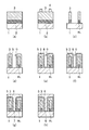
G 溝状領域
1 層間絶縁膜
2 配線膜
3 マスク絶縁膜
4 レジスト
5 サイドウォール絶縁膜
6 ライナー膜
7 ポリシラザン
8 シリコン酸化膜
Claims (8)
- 基板、前記基板表面に形成された溝状領域、及び前記溝状領域に埋設されたシリコン酸化膜を有する半導体装置の製造方法であって、
前記溝状領域を含む前記基板の表面を覆うライナー膜を形成するライナー膜形成工程と、
前記ライナー膜の表面を水洗する水洗工程と、
前記水洗後の残留水分を除去する水分除去工程と、
前記基板表面にポリシラザン溶液をスピンコートにより塗布する塗布工程と、
アニールにより前記ポリシラザン溶液を前記シリコン酸化膜に改質する改質工程と
を備えることを特徴とする半導体装置の製造方法。 - 前記水分除去工程は、前記基板を熱し、前記残留水分を気化させることによって実施される
ことを特徴とする請求項1に記載の半導体装置の製造方法。 - 前記塗布工程及び前記改質工程は、ホットプレートを備えるSOD塗布機によって実施され、
前記水分除去工程及び前記改質工程では、前記ホットプレートによって前記基板を熱する
ことを特徴とする請求項2に記載の半導体装置の製造方法。 - 前記水分除去工程では、前記アニールより高い温度で前記基板を熱する
ことを特徴とする請求項2又は3に記載の半導体装置の製造方法。 - 前記水分除去工程と前記塗布工程の間に、前記基板を冷ます冷却工程をさらに備える
ことを特徴とする請求項1乃至4のいずれか一項に記載の半導体装置の製造方法。 - 前記塗布工程は、
前記ポリシラザン溶液を滴下するディスペンス工程と、
前記ディスペンス工程で滴下した前記ポリシラザン溶液を前記基板表面に拡散するリフロー工程と、
前記リフロー工程の実施後、前記ポリシラザン溶液を除去するキャスティング工程とを有し、
前記リフロー工程は、3秒以上にわたって実施される
ことを特徴とする請求項1乃至5のいずれか一項に記載の半導体装置の製造方法。 - 前記ディスペンス工程では、前記基板を第1の回転数で回転させた状態で前記滴下を実施し、
前記リフロー工程では、前記基板を第2の回転数で回転させた状態で前記拡散を実施し、
前記キャスティング工程では、前記基板を第3の回転数で回転させた状態で前記除去を実施し、
前記第2の回転数は、前記第1及び第3の回転数より低い
ことを特徴とする請求項6に記載の半導体装置の製造方法。 - 前記第2の回転数は200rpm以下であり、前記第1及び第3の回転数は1000rpm以上である
ことを特徴とする請求項7に記載の半導体装置の製造方法。
Priority Applications (2)
| Application Number | Priority Date | Filing Date | Title |
|---|---|---|---|
| JP2011001305A JP2012142528A (ja) | 2011-01-06 | 2011-01-06 | 半導体装置の製造方法 |
| US13/341,449 US20120178265A1 (en) | 2011-01-06 | 2011-12-30 | Method of manufacturing semiconductor device using sod method |
Applications Claiming Priority (1)
| Application Number | Priority Date | Filing Date | Title |
|---|---|---|---|
| JP2011001305A JP2012142528A (ja) | 2011-01-06 | 2011-01-06 | 半導体装置の製造方法 |
Publications (1)
| Publication Number | Publication Date |
|---|---|
| JP2012142528A true JP2012142528A (ja) | 2012-07-26 |
Family
ID=46455598
Family Applications (1)
| Application Number | Title | Priority Date | Filing Date |
|---|---|---|---|
| JP2011001305A Pending JP2012142528A (ja) | 2011-01-06 | 2011-01-06 | 半導体装置の製造方法 |
Country Status (2)
| Country | Link |
|---|---|
| US (1) | US20120178265A1 (ja) |
| JP (1) | JP2012142528A (ja) |
Families Citing this family (5)
| Publication number | Priority date | Publication date | Assignee | Title |
|---|---|---|---|---|
| KR102352232B1 (ko) | 2015-06-15 | 2022-01-17 | 삼성전자주식회사 | 콘택 구조체들을 갖는 반도체 소자의 제조 방법 |
| US9847245B1 (en) | 2016-06-16 | 2017-12-19 | Samsung Electronics Co., Ltd. | Filling processes |
| US10329452B2 (en) * | 2016-06-21 | 2019-06-25 | Honeywell International Inc. | Materials and spin coating methods suitable for advanced planarization applications |
| CN110890268A (zh) * | 2018-09-10 | 2020-03-17 | 长鑫存储技术有限公司 | 晶圆镀膜方法与设备 |
| CN117524851B (zh) * | 2024-01-03 | 2024-05-14 | 长鑫新桥存储技术有限公司 | 氧化硅薄膜的制备方法及半导体结构 |
Citations (8)
| Publication number | Priority date | Publication date | Assignee | Title |
|---|---|---|---|---|
| JPS62115745A (ja) * | 1985-11-15 | 1987-05-27 | Nec Corp | 半導体装置の製造方法 |
| JP2000021873A (ja) * | 1998-06-26 | 2000-01-21 | Fujitsu Ltd | 積層構造、配線構造、その製造方法、及び半導体装置 |
| JP2005340802A (ja) * | 2004-04-28 | 2005-12-08 | Semiconductor Energy Lab Co Ltd | 半導体装置及び表示装置の作製方法 |
| JP2006128638A (ja) * | 2004-09-29 | 2006-05-18 | Semiconductor Energy Lab Co Ltd | 半導体装置及びその作製方法 |
| WO2007083654A1 (ja) * | 2006-01-18 | 2007-07-26 | Az Electronic Materials (Japan) K.K. | シリカ質膜の製造法およびそれにより製造されたシリカ質膜付き基板 |
| JP2010098293A (ja) * | 2008-09-22 | 2010-04-30 | Elpida Memory Inc | 半導体装置 |
| JP2010166026A (ja) * | 2008-12-16 | 2010-07-29 | Elpida Memory Inc | 半導体装置及びその製造方法 |
| JP2010186938A (ja) * | 2009-02-13 | 2010-08-26 | Asahi Kasei E-Materials Corp | ポリシロキサン系トレンチ埋め込み用縮合反応物及びトレンチ埋め込み膜の製造方法 |
Family Cites Families (5)
| Publication number | Priority date | Publication date | Assignee | Title |
|---|---|---|---|---|
| KR100512167B1 (ko) * | 2001-03-12 | 2005-09-02 | 삼성전자주식회사 | 트렌치 소자 분리형 반도체 장치 및 트렌치형 소자 분리막형성방법 |
| JP2003156858A (ja) * | 2001-11-22 | 2003-05-30 | Tokyo Electron Ltd | 基板処理方法及び基板処理システム |
| JP5091722B2 (ja) * | 2008-03-04 | 2012-12-05 | 東京エレクトロン株式会社 | 塗布処理方法、プログラム、コンピュータ記憶媒体及び塗布処理装置 |
| JP2010283256A (ja) * | 2009-06-08 | 2010-12-16 | Toshiba Corp | 半導体装置およびnand型フラッシュメモリの製造方法 |
| US8105956B2 (en) * | 2009-10-20 | 2012-01-31 | Micron Technology, Inc. | Methods of forming silicon oxides and methods of forming interlevel dielectrics |
-
2011
- 2011-01-06 JP JP2011001305A patent/JP2012142528A/ja active Pending
- 2011-12-30 US US13/341,449 patent/US20120178265A1/en not_active Abandoned
Patent Citations (8)
| Publication number | Priority date | Publication date | Assignee | Title |
|---|---|---|---|---|
| JPS62115745A (ja) * | 1985-11-15 | 1987-05-27 | Nec Corp | 半導体装置の製造方法 |
| JP2000021873A (ja) * | 1998-06-26 | 2000-01-21 | Fujitsu Ltd | 積層構造、配線構造、その製造方法、及び半導体装置 |
| JP2005340802A (ja) * | 2004-04-28 | 2005-12-08 | Semiconductor Energy Lab Co Ltd | 半導体装置及び表示装置の作製方法 |
| JP2006128638A (ja) * | 2004-09-29 | 2006-05-18 | Semiconductor Energy Lab Co Ltd | 半導体装置及びその作製方法 |
| WO2007083654A1 (ja) * | 2006-01-18 | 2007-07-26 | Az Electronic Materials (Japan) K.K. | シリカ質膜の製造法およびそれにより製造されたシリカ質膜付き基板 |
| JP2010098293A (ja) * | 2008-09-22 | 2010-04-30 | Elpida Memory Inc | 半導体装置 |
| JP2010166026A (ja) * | 2008-12-16 | 2010-07-29 | Elpida Memory Inc | 半導体装置及びその製造方法 |
| JP2010186938A (ja) * | 2009-02-13 | 2010-08-26 | Asahi Kasei E-Materials Corp | ポリシロキサン系トレンチ埋め込み用縮合反応物及びトレンチ埋め込み膜の製造方法 |
Also Published As
| Publication number | Publication date |
|---|---|
| US20120178265A1 (en) | 2012-07-12 |
Similar Documents
| Publication | Publication Date | Title |
|---|---|---|
| US8603892B2 (en) | Method of manufacturing a semiconductor device | |
| US20150357232A1 (en) | Method for manufacturing semiconductor device | |
| CN100373624C (zh) | 半导体存储器装置及其制造方法 | |
| US20070207590A1 (en) | Manufacturing method of semiconductor device | |
| US20080157266A1 (en) | Sti liner modification method | |
| TW200534389A (en) | Method for fabricating semiconductor device capable of preventing damage by wet cleaning process | |
| US7238586B2 (en) | Seamless trench fill method utilizing sub-atmospheric pressure chemical vapor deposition technique | |
| JP2012142528A (ja) | 半導体装置の製造方法 | |
| JP2009076615A (ja) | 半導体装置の製造方法 | |
| US8772153B2 (en) | Semiconductor device with air gap therein and manufacturing method thereof | |
| US7892984B2 (en) | Reduction of defects formed on the surface of a silicon oxynitride film | |
| CN101752242A (zh) | 绝缘层以及使用其的半导体器件的制造方法 | |
| KR100531467B1 (ko) | 반도체 소자의 층간절연막 형성 방법 | |
| TWI287258B (en) | Method for fabricating semiconductor device | |
| JP3629179B2 (ja) | 半導体装置の製造方法 | |
| US6887767B2 (en) | Method for manufacturing semiconductor device | |
| US6245688B1 (en) | Dry Air/N2 post treatment to avoid the formation of B/P precipitation after BPSG film deposition | |
| KR100755073B1 (ko) | 반도체 소자의 콘택 홀 형성 방법 | |
| KR100869852B1 (ko) | 반도체 소자의 소자분리막 형성방법 | |
| JP5640448B2 (ja) | 半導体装置の製造方法 | |
| KR20090045679A (ko) | 반도체 소자 제조 방법 | |
| JP2008041977A (ja) | 半導体回路装置の製造方法 | |
| KR100695420B1 (ko) | 반도체 소자의 컨택 플러그 형성방법 | |
| KR101082107B1 (ko) | 소자분리층을 포함하는 반도체 소자 및 제조 방법 | |
| KR20090106883A (ko) | 반도체 소자의 제조방법 |
Legal Events
| Date | Code | Title | Description |
|---|---|---|---|
| A711 | Notification of change in applicant |
Free format text: JAPANESE INTERMEDIATE CODE: A711 Effective date: 20130730 |
|
| A521 | Request for written amendment filed |
Free format text: JAPANESE INTERMEDIATE CODE: A523 Effective date: 20130822 |
|
| A621 | Written request for application examination |
Free format text: JAPANESE INTERMEDIATE CODE: A621 Effective date: 20131218 |
|
| A977 | Report on retrieval |
Free format text: JAPANESE INTERMEDIATE CODE: A971007 Effective date: 20141113 |
|
| A131 | Notification of reasons for refusal |
Free format text: JAPANESE INTERMEDIATE CODE: A131 Effective date: 20141118 |
|
| A02 | Decision of refusal |
Free format text: JAPANESE INTERMEDIATE CODE: A02 Effective date: 20150414 |