JP2012146529A - Thin film display device inspection/correction method and inspection/correction apparatus - Google Patents

Thin film display device inspection/correction method and inspection/correction apparatus Download PDF

Info

Publication number
JP2012146529A
JP2012146529A JP2011004234A JP2011004234A JP2012146529A JP 2012146529 A JP2012146529 A JP 2012146529A JP 2011004234 A JP2011004234 A JP 2011004234A JP 2011004234 A JP2011004234 A JP 2011004234A JP 2012146529 A JP2012146529 A JP 2012146529A
Authority
JP
Japan
Prior art keywords
light emitting
emitting layer
defect
light
inspection
Prior art date
Legal status (The legal status is an assumption and is not a legal conclusion. Google has not performed a legal analysis and makes no representation as to the accuracy of the status listed.)
Pending
Application number
JP2011004234A
Other languages
Japanese (ja)
Inventor
Toshiyuki Nakao
敏之 中尾
Shigenobu Maruyama
重信 丸山
Fumio Kataoka
文雄 片岡
Current Assignee (The listed assignees may be inaccurate. Google has not performed a legal analysis and makes no representation or warranty as to the accuracy of the list.)
Hitachi High Tech Corp
Original Assignee
Hitachi High Technologies Corp
Hitachi High Tech Corp
Priority date (The priority date is an assumption and is not a legal conclusion. Google has not performed a legal analysis and makes no representation as to the accuracy of the date listed.)
Filing date
Publication date
Application filed by Hitachi High Technologies Corp, Hitachi High Tech Corp filed Critical Hitachi High Technologies Corp
Priority to JP2011004234A priority Critical patent/JP2012146529A/en
Priority to TW100141091A priority patent/TW201238112A/en
Priority to CN2011104102053A priority patent/CN102593378A/en
Priority to KR1020110131719A priority patent/KR101368150B1/en
Publication of JP2012146529A publication Critical patent/JP2012146529A/en
Pending legal-status Critical Current

Links

Images
Classifications

    • HELECTRICITY
    • H10SEMICONDUCTOR DEVICES; ELECTRIC SOLID-STATE DEVICES NOT OTHERWISE PROVIDED FOR
    • H10KORGANIC ELECTRIC SOLID-STATE DEVICES
    • H10K71/00Manufacture or treatment specially adapted for the organic devices covered by this subclass
    • H10K71/70Testing, e.g. accelerated lifetime tests
    • GPHYSICS
    • G01MEASURING; TESTING
    • G01RMEASURING ELECTRIC VARIABLES; MEASURING MAGNETIC VARIABLES
    • G01R31/00Arrangements for testing electric properties; Arrangements for locating electric faults; Arrangements for electrical testing characterised by what is being tested not provided for elsewhere
    • G01R31/26Testing of individual semiconductor devices
    • G01R31/2607Circuits therefor
    • G01R31/2632Circuits therefor for testing diodes
    • G01R31/2635Testing light-emitting diodes, laser diodes or photodiodes
    • HELECTRICITY
    • H10SEMICONDUCTOR DEVICES; ELECTRIC SOLID-STATE DEVICES NOT OTHERWISE PROVIDED FOR
    • H10KORGANIC ELECTRIC SOLID-STATE DEVICES
    • H10K71/00Manufacture or treatment specially adapted for the organic devices covered by this subclass
    • H10K71/861Repairing

Landscapes

  • Physics & Mathematics (AREA)
  • Engineering & Computer Science (AREA)
  • Manufacturing & Machinery (AREA)
  • Optics & Photonics (AREA)
  • General Physics & Mathematics (AREA)
  • Electroluminescent Light Sources (AREA)
  • Devices For Indicating Variable Information By Combining Individual Elements (AREA)

Abstract

【課題】
カラーフィルタ方式のOLEDパネルでも、単一波長で、かつ高い信頼性で検査・修正が可能であり、歩留まりを向上させることのできる薄膜表示素子の検査修正方法及び検査修正装置を提供する。
【解決手段】
発光層の上に形成された金属電極膜と発光層の金属電極膜と反対の側に形成された透明電極膜とを有する薄膜表示素子の発光の状態を検査して不良箇所を修正する方法及びその装置を、金属電極と透明電極とに電力を印加して発光層を発光させ、この発光層の発光の状態を金属電極に対して透明電極の側から観察して発光層で発光していない位置を検出し、この検出した発光層で発光していない位置の情報に基づいて金属電極に透明電極と反対の側からレーザを照射して発光層で発光していない位置の上方の金属電極膜を除去するように構成した。
【選択図】 図8
【Task】
A thin film display element inspection and correction method and inspection correction apparatus that can perform inspection and correction with a single wavelength and high reliability even with a color filter type OLED panel and can improve the yield are provided.
[Solution]
A method for inspecting a light emitting state of a thin film display element having a metal electrode film formed on a light emitting layer and a transparent electrode film formed on the light emitting layer on the opposite side of the metal electrode film, and correcting a defective portion, and The device applies power to the metal electrode and the transparent electrode to cause the light emitting layer to emit light, and the light emission state of the light emitting layer is observed from the transparent electrode side with respect to the metal electrode, and the light emitting layer does not emit light. The metal electrode film above the position where the position is detected and the light is not emitted from the light emitting layer by irradiating the metal electrode with the laser from the side opposite to the transparent electrode based on the information of the position where the light emitting layer does not emit light Was configured to be removed.
[Selection] Figure 8

Description

本発明はFPDの非点灯画素を検査し、非点灯画素の修正を行う検査修正方法および検査修正装置に関し、特にOLEDパネルなどの薄膜表示素子の検査、集積に適した薄膜表示素子の検査修正方法及び検査修正装置に関する。   The present invention relates to an inspection correction method and an inspection correction apparatus for inspecting non-lighting pixels of an FPD and correcting the non-lighting pixels, and more particularly to inspection of thin film display elements such as OLED panels and inspection correction methods for thin film display elements suitable for integration. And an inspection correction apparatus.

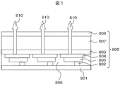
FPD(Flat Panel Display)の一種類である有機EL(Electro Luminescence)表示装置や照明装置に用いられるOLED(Organic Light Emitting Diode)パネルは、光の取り出し方向の違いにより、トップエミッション型とボトムエミッション型の2つに大別され、トップエミッション型は一般的に図1に示すようなパネル構造をしている。即ち、トップエミッション型は、ガラス基板801上にTFT層(Thin Film Transistor)802が形成され、その上に透明電極803・有機発光層804・金属電極805・絶縁層806が積層され、樹脂807と封止ガラス808で封止されている。透明電極803と金属電極805の間に電圧を印加し、有機発光層804の内部で電子とホールが結合することで発光する。この構成において、トップエミッション型は、ガラス基板808と逆側から光810を取り出す。一方、ボトムエミッション型は、図2に示すように、ガラス基板801の側から光820を取り出す。図2に示したボトムエミッション型はTFT回路形成部以外の領域から光を取り出す必要があるため開口率は低いが、大型化には有利な構造である。一方、図1に示したトップエミッション型は、TFT回路形成部とは逆側に光を取り出すため高い開口率を有するが、大型化は困難である。よって、トップエミッション型は携帯電話などの小型パネルに、ボトムエミッション型はテレビなどの大型パネルに使用されることが多い。   OLED (Organic Light Emitting Diode) panels used in organic EL (Electro Luminescence) display devices and lighting devices, which are one type of FPD (Flat Panel Display), are different from the top emission type and bottom emission type depending on the direction of light extraction. The top emission type generally has a panel structure as shown in FIG. That is, in the top emission type, a TFT layer (Thin Film Transistor) 802 is formed on a glass substrate 801, and a transparent electrode 803, an organic light emitting layer 804, a metal electrode 805, and an insulating layer 806 are laminated thereon, and a resin 807 Sealed with sealing glass 808. A voltage is applied between the transparent electrode 803 and the metal electrode 805, and light is emitted by combining electrons and holes inside the organic light emitting layer 804. In this configuration, the top emission type extracts light 810 from the side opposite to the glass substrate 808. On the other hand, the bottom emission type takes out light 820 from the glass substrate 801 side as shown in FIG. The bottom emission type shown in FIG. 2 has a low aperture ratio because it is necessary to take out light from a region other than the TFT circuit formation portion, but is a structure advantageous for an increase in size. On the other hand, the top emission type shown in FIG. 1 has a high aperture ratio because light is extracted on the side opposite to the TFT circuit forming portion, but it is difficult to increase the size. Therefore, the top emission type is often used for a small panel such as a mobile phone, and the bottom emission type is often used for a large panel such as a television.

有機発光層804の膜厚は100nm程度であり、非常に薄いことがOLEDパネルの特徴である。製造プロセスの途中で装置発塵などにより異物が混入し、透明電極803と金属電極805がショートすると、該当画素が非点灯となる。OLEDパネルの大型化に伴い、パネルあたりの異物数が増加し、非点灯画素が増えるため、歩留まり向上のために非点灯画素修正のニーズが高まっている。   The thickness of the organic light emitting layer 804 is about 100 nm, and it is a feature of the OLED panel that it is very thin. If a foreign substance is mixed due to device dust generation during the manufacturing process and the transparent electrode 803 and the metal electrode 805 are short-circuited, the corresponding pixel is turned off. As the size of the OLED panel increases, the number of foreign objects per panel increases and the number of non-lighted pixels increases. Therefore, the need for correcting non-lighted pixels is increasing in order to improve the yield.

OLEDパネルの非点灯画素の修正技術としてはこれまでに特許文献1、特許文献2に記載の技術が知られている。   As correction techniques for non-lighting pixels of the OLED panel, techniques described in Patent Document 1 and Patent Document 2 have been known so far.

特許文献1記載の技術によれば、非点灯画素に対応する金属電極からショートの発生領域がレーザで除去される。これにより部分的に除去された金属電極と透明電極との間の有機発光層が発光可能となり、非点灯画素が修復される。   According to the technique described in Patent Document 1, a short generation region is removed by a laser from a metal electrode corresponding to a non-lighted pixel. As a result, the organic light emitting layer between the partially removed metal electrode and the transparent electrode can emit light, and non-lighted pixels are restored.

特許文献2記載の技術によれば、観察光学系で非点灯画素内の異物の位置を検出し、レーザで異物の周囲を帯状に除去する。これにより、異物存在箇所が孤立化され、ショートが解消され、非点灯画素が修復される。   According to the technique described in Patent Document 2, the position of a foreign substance in a non-lighted pixel is detected by an observation optical system, and the periphery of the foreign substance is removed in a belt shape by a laser. As a result, a foreign substance existing location is isolated, a short circuit is eliminated, and a non-lighted pixel is repaired.

特許文献1、2ともに、画素が修復されても、レーザ照射により画素内で非発光となる部分が発生するため、非発光となる面積を小さく抑える必要がある。   In both Patent Documents 1 and 2, even if the pixel is repaired, a portion that does not emit light is generated in the pixel due to laser irradiation, and thus it is necessary to reduce the area that does not emit light.

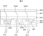
一方、ディスプレイの色表示方式は大別して3種類であり、3色方式(図3)、色変換方式(図4)、カラーフィルタ方式(図5)である。図3〜図5はボトムエミッション型を前提として表記している。図3の3色方式は赤色光811を発光する有機材料膜8041、緑色光812を発光する有機材料膜8042、青色光813を発光する有機材料膜8043をそれぞれ塗り分ける方式であり、色純度を向上させるため、カラーフィルタを併用する場合もある。図4の色変換方式は、青色発光有機材料膜8044を用い、その青色光814を赤色光に色変換する色変換層8091と緑色光に色変換する色変換層8092に通すことにより、赤色光815・緑色光816を得る方式である。図5のカラーフィルタ方式は白色発光有機材料膜8045を用い、赤色光に色変換するカラーフィルタ8093、緑色光に色変換するカラーフィルタ8094、青色光に色変換するカラーフィルタ8095を通すことで赤色光817・緑色光818・青色光819を得る方式である。   On the other hand, there are roughly three types of display color display methods: a three-color method (FIG. 3), a color conversion method (FIG. 4), and a color filter method (FIG. 5). 3 to 5 are shown assuming a bottom emission type. The three-color system in FIG. 3 is a system in which an organic material film 8041 that emits red light 811, an organic material film 8042 that emits green light 812, and an organic material film 8043 that emits blue light 813 are separately applied. In order to improve, a color filter may be used together. The color conversion method of FIG. 4 uses a blue light emitting organic material film 8044 and passes the blue light 814 through a color conversion layer 8091 that converts color into red light and a color conversion layer 8092 that converts color into green light. 815 is a method for obtaining green light 816. 5 uses a white light-emitting organic material film 8045 and passes through a color filter 8093 for color conversion to red light, a color filter 8094 for color conversion to green light, and a color filter 8095 for color conversion to blue light. In this method, light 817, green light 818, and blue light 819 are obtained.

図3に示した3色方式では3種類の有機材料を塗り分ける必要があり、塗りわけには現在は真空蒸着が利用されている。しかし真空蒸着ではシャドウマスクの熱膨張による成膜むらが生じ、パネル大型化への対応が困難である。別の塗りわけ方法として印刷技術もあるが、こちらは高分子青色発光有機材料の開発が遅れている。図4の色変換方式では、青色発光有機材料の開発が赤・緑色発光有機材料に比べて困難であり、かつ色変換効率の低さが課題となっている。図5のカラーフィルタ方式では、白色発光有機材料のみを使用するため、有機材料をぬりわける必要がない。カラーフィルタでの光量ロスは発生するが、カラーフィルタの製造工程に関しては液晶パネルで培った技術も転用することができ、パネルの大型化にはカラーフィルタ方式が主流となると予測できる。   In the three-color system shown in FIG. 3, it is necessary to coat three types of organic materials separately, and vacuum deposition is currently used for coating. However, vacuum deposition causes uneven film formation due to thermal expansion of the shadow mask, and it is difficult to cope with an increase in the panel size. There is also a printing technique as another coating method, but this is behind the development of a polymer blue light-emitting organic material. In the color conversion method shown in FIG. 4, it is difficult to develop a blue light emitting organic material as compared with red and green light emitting organic materials, and low color conversion efficiency is a problem. In the color filter system shown in FIG. 5, since only a white light emitting organic material is used, it is not necessary to remove the organic material. Although the light quantity loss occurs in the color filter, the technology cultivated in the liquid crystal panel can be diverted for the manufacturing process of the color filter, and it can be predicted that the color filter system will become the mainstream for the enlargement of the panel.

特開2001−118684号公報JP 2001-118684 A 特開2005−276600号公報JP 2005-276600 A

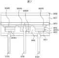
カラーフィルタは赤緑青で分光透過率が異なる。図6にカラーフィルタの分光透過率の一例を示す。601は赤色カラーフィルタ8093の分光透過率特性、602は緑色カラーフィルタ8094の分光透過率特性、603は青色カラーフィルタ8095の分光透過率特性を示す。各カラーフィルタ8093,8094及び8095は、透過させる光の波長帯域以外では透過率が極めて低い。塗布材料や膜厚によって透過率に多少の差異は存在するがほぼ同様の傾向を示す。例えば図7のように波長532nmのレーザ830を使用した場合、緑のカラーフィルタ8094では透過率が高いため、金属電極803まで光を到達させることができ、金属電極803を加工することができるが、赤と青のカラーフィルタ8093及び8095では大半のエネルギがカラーフィルタ8093及び8095に吸収され、金属電極803まで光を到達させることができない。また、金属電極803に高エネルギの光を到達させるために照射エネルギを増加させると、金属電極803よりもカラーフィルタ8093及び8095が先に融解してしまう。   The color filters are red, green, and blue and have different spectral transmittances. FIG. 6 shows an example of the spectral transmittance of the color filter. Reference numeral 601 denotes a spectral transmittance characteristic of the red color filter 8093, 602 denotes a spectral transmittance characteristic of the green color filter 8094, and 603 denotes a spectral transmittance characteristic of the blue color filter 8095. Each of the color filters 8093, 8094, and 8095 has an extremely low transmittance except for the wavelength band of light to be transmitted. Although there are some differences in transmittance depending on the coating material and film thickness, the same tendency is shown. For example, when a laser 830 having a wavelength of 532 nm is used as shown in FIG. 7, the green color filter 8094 has high transmittance, so that light can reach the metal electrode 803 and the metal electrode 803 can be processed. In the red and blue color filters 8093 and 8095, most of the energy is absorbed by the color filters 8093 and 8095, and light cannot reach the metal electrode 803. Further, when the irradiation energy is increased in order to allow the high energy light to reach the metal electrode 803, the color filters 8093 and 8095 are melted earlier than the metal electrode 803.

特許文献1および特許文献2に記載されている発明では、金属電極803に対して透明電極805の側よりレーザ照射を行い、不良箇所に対応する金属電極803の一部を削除する修正を行っている。赤・緑・青のカラーフィルタ8093乃至8095のどれか1つでは高い透過率を有する波長のレーザを使用しても、他の2つのカラーフィルタでは透過率が低く、透明電極805の側からのレーザ照射では単一波長のレーザで全ての画素の修正を行うことはできない。   In the invention described in Patent Document 1 and Patent Document 2, the metal electrode 803 is irradiated with laser from the transparent electrode 805 side, and a correction is made to delete a part of the metal electrode 803 corresponding to the defective portion. Yes. Even if one of the red, green, and blue color filters 8093 to 8095 uses a laser having a wavelength having a high transmittance, the other two color filters have a low transmittance, and the light from the transparent electrode 805 side is low. With laser irradiation, it is not possible to correct all pixels with a single wavelength laser.

一方、カラーフィルタ方式のOLEDパネルに対しては、金属電極803に対して透明電極805の側から異物の検出を行い、透明電極805と反対側から金属電極803にレーザ照射を行えば、カラーフィルタ8093乃至8095の分光透過率を無視して金属電極803を加工できる。しかし、単に異物検出手段とレーザ加工手段とを接続しただけでは、異物検出手段で検出した異物検出位置とレーザ加工手段によるレーザ加工位置をミクロン単位で合わせることは難しい。さらに、OLEDパネルの透明電極805の側を上向きにして異物検出手段で異物を検出した後、金属電極803の側からレーザ照射を行うためには、OLEDパネルを裏返してからレーザ照射を行う必要があり、装置の複雑化・大型化、ラインタクトの延長を招く。また、金属電極803の側からでは異物を検出できないため、あらかじめ求められた座標へ機械的にOLEDパネルを移動させることになる。しかし、OLEDパネルを裏返すときに発生する位置ずれやステージの移動誤差などにより、所望の位置にOLEDパネルを移動させることができず、レーザ照射を行う位置がずれ、修正に失敗するケースが増加するという課題があった。   On the other hand, for a color filter type OLED panel, if a foreign object is detected from the transparent electrode 805 side with respect to the metal electrode 803 and laser irradiation is performed on the metal electrode 803 from the opposite side of the transparent electrode 805, the color filter The metal electrode 803 can be processed ignoring the spectral transmittance of 8093 to 8095. However, simply connecting the foreign matter detection means and the laser processing means makes it difficult to match the foreign matter detection position detected by the foreign matter detection means and the laser processing position by the laser processing means in units of microns. Furthermore, in order to perform laser irradiation from the metal electrode 803 side after detecting the foreign matter with the foreign matter detection means with the transparent electrode 805 side of the OLED panel facing upward, it is necessary to turn the OLED panel over and then perform laser irradiation. Yes, the equipment becomes complicated and large, and the line tact is extended. Further, since the foreign matter cannot be detected from the metal electrode 803 side, the OLED panel is mechanically moved to the coordinates determined in advance. However, the OLED panel cannot be moved to a desired position due to a positional deviation or a stage movement error that occurs when the OLED panel is turned over, and the number of cases where the laser irradiation position is shifted and the correction fails increases. There was a problem.

本発明は、上記した課題を解決してカラーフィルタ方式のOLEDパネルでも、単一波長で、かつ高い信頼性で検査・修正が可能であり、歩留まりを向上させることのできる薄膜表示素子の検査修正方法及び検査修正装置を提供することを目的とする。   The present invention solves the above-mentioned problems, and even with a color filter type OLED panel, it is possible to perform inspection and correction with a single wavelength and with high reliability, and to perform inspection and correction of a thin film display element capable of improving the yield. It is an object to provide a method and an inspection correction apparatus.

上記した課題を解決するために、本発明では、発光層の上に形成された金属電極膜と発光層の金属電極膜と反対の側に形成された透明電極膜とを有する薄膜表示素子の発光の状態を検査して不良箇所を修正する方法において、金属電極と透明電極とに電力を印加して発光層を発光させ、この発光層の発光の状態を金属電極に対して透明電極の側から観察して発光層で発光していない位置を検出し、この検出した発光層で発光していない位置の情報に基づいて金属電極に透明電極と反対の側からレーザを照射して発光層で発光していない位置の上方の金属電極膜を除去するようにした。   In order to solve the above-described problems, in the present invention, light emission of a thin film display element having a metal electrode film formed on a light emitting layer and a transparent electrode film formed on the side of the light emitting layer opposite to the metal electrode film. In the method of inspecting the state of the defect and correcting the defective portion, power is applied to the metal electrode and the transparent electrode to cause the light emitting layer to emit light, and the light emitting state of the light emitting layer is changed from the transparent electrode side to the metal electrode. The position where light is not emitted from the light emitting layer is observed and light is emitted from the light emitting layer by irradiating the metal electrode with a laser from the side opposite to the transparent electrode based on the information on the position where light is not emitted from the detected light emitting layer. The metal electrode film above the position where it was not removed was removed.

また、上記した課題を解決するために、本発明では、発光層の上に形成された金属電極膜と発光層の金属電極膜と反対の側に形成された透明電極膜とを有する薄膜表示素子の発光の状態を検査して不良箇所を修正する装置を、薄膜表示素子の金属電極と透明電極とに電力を印加して発光層を発光させる電力印加手段と、この電力印加手段により電力が印加された薄膜表示素子の発光層の発光の状態を金属電極に対して透明電極の側から観察して発光層で発光していない位置を検出する発光状態観察手段と、この発光状態観察手段で検出した発光層で発光していない位置の情報に基づいて金属電極に透明電極と反対の側からレーザを照射して発光層で発光していない位置の上方の金属電極膜を除去する薄膜除去加工手段とを備えて構成した。   In order to solve the above-described problems, in the present invention, a thin film display element having a metal electrode film formed on a light emitting layer and a transparent electrode film formed on the light emitting layer on the side opposite to the metal electrode film. A device for inspecting the state of light emission and correcting a defective portion, applying power to the metal electrode and the transparent electrode of the thin film display element to cause the light emitting layer to emit light, and applying power by the power application unit A light emission state observation means for observing the light emission state of the light emitting layer of the thin film display element from the transparent electrode side with respect to the metal electrode and detecting a position where the light emission layer does not emit light, and the light emission state observation means Thin film removing means for removing the metal electrode film above the position where the light emitting layer does not emit light by irradiating the metal electrode with a laser from the side opposite to the transparent electrode based on the information on the position where the light emitting layer does not emit light And configured.

本発明によれば,カラーフィルタ方式のOLEDパネル構造において、単一波長のレーザで非点灯画素の修正が可能となり、高い生産性の維持と歩留まり向上に貢献できる。   According to the present invention, in a color filter type OLED panel structure, a non-lighted pixel can be corrected with a single wavelength laser, which can contribute to maintaining high productivity and improving yield.

トップエミッション型OLEDの構造の断面図である。It is sectional drawing of the structure of top emission type OLED. ボトムエミッション型OLEDの構造の断面図である。It is sectional drawing of the structure of bottom emission type OLED. 3色方式のOLEDの構造の断面図である。It is sectional drawing of the structure of OLED of a 3 color system. 色変換方式のOLEDの構造の断面図である。It is sectional drawing of the structure of OLED of a color conversion system. カラーフィルタ方式のOLEDの構造の断面図である。It is sectional drawing of the structure of OLED of a color filter system. 一般的なカラーフィルタの分光透過率特性を示すグラフである。It is a graph which shows the spectral transmittance characteristic of a general color filter. カラーフィルタ方式OLEDパネルにレーザ照射を行う場合のOLEDの構造の断面図である。It is sectional drawing of the structure of OLED when performing laser irradiation to a color filter system OLED panel. 本発明の実施例に係る薄膜表示装置の検査修正装置の概略構成を示すブロック図である。It is a block diagram which shows schematic structure of the test | inspection correction apparatus of the thin film display apparatus which concerns on the Example of this invention. OLED基板の平面図である。It is a top view of an OLED substrate. 本発明の実施例に係る薄膜表示装置の検査修正装置でテーブルに長方形の切り欠きを有する点灯検査部の概略の構成を正面から見たブロック図である。It is the block diagram which looked at the schematic structure of the lighting test | inspection part which has a rectangular notch in a table with the test | inspection correction apparatus of the thin film display apparatus which concerns on the Example of this invention from the front. 本発明の実施例に係る薄膜表示装置の検査修正装置で点灯検査部の長方形の切り欠きを有するテーブルを上面から見たブロック図である。It is the block diagram which looked at the table which has the rectangular notch of the lighting inspection part from the upper surface in the inspection correction apparatus of the thin film display apparatus which concerns on the Example of this invention. 本発明の実施例に係る薄膜表示装置の検査修正装置でテーブルにスリット状の切り欠きを有する点灯検査部の概略の構成を正面から見たブロック図である。It is the block diagram which looked at the schematic structure of the lighting test | inspection part which has a slit-shaped notch in a table with the test | inspection correction apparatus of the thin film display apparatus which concerns on the Example of this invention from the front. 本発明の実施例に係る薄膜表示装置の検査修正装置で点灯検査部のスリット状の切り欠きを有するテーブルを上面から見たブロック図点灯検査時のスキャン方法の説明図である。It is explanatory drawing of the scanning method at the time of the block diagram lighting test | inspection which looked at the table which has the slit-shaped notch of the lighting test | inspection part from the upper surface in the test | inspection correction apparatus of the thin film display apparatus which concerns on the Example of this invention. 点灯検査部の処理の流れを示すフロー図である。It is a flowchart which shows the flow of a process of a lighting test | inspection part. 点灯検査結果の一例を示すOLED基板の平面図である。It is a top view of the OLED board which shows an example of a lighting inspection result. (a)欠陥検査部の視野の中心に修正前の欠陥を位置したOLED基板の非点灯画素の平面図、(b)修正前の欠陥を含むOLEDの構造の非点灯画素の断面図、(c)欠陥検査部の視野の中心にリング状の加工を施して修正した後の欠陥を位置したOLED基板の非点灯画素の平面図、(d)リング状の加工を施して修正した後の欠陥を含むOLEDの構造の断面図である。(A) A plan view of a non-lighted pixel of an OLED substrate in which a defect before correction is located in the center of a visual field of a defect inspection unit, (b) a cross-sectional view of a non-lighted pixel of an OLED structure including the defect before correction, (c) ) A plan view of the non-lighted pixel of the OLED substrate where the defect after the ring-shaped processing is corrected at the center of the visual field of the defect inspection portion, (d) the defect after the correction is performed by applying the ring-shaped processing It is sectional drawing of the structure of OLED containing. (a)欠陥検査部の視野の中心に修正前の欠陥を位置したOLED基板の非点灯画素の平面図、(b)修正前の欠陥を含むOLEDの構造の非点灯画素の断面図、(c)欠陥検査部の視野の中心に円形の加工を施して修正した後の欠陥を位置したOLED基板の非点灯画素の平面図、(d)リング状の加工を施して修正した後の欠陥を含むOLEDの構造の断面図である。(A) A plan view of a non-lighted pixel of an OLED substrate in which a defect before correction is located in the center of a visual field of a defect inspection unit, (b) a cross-sectional view of a non-lighted pixel of an OLED structure including the defect before correction, (c) ) A plan view of the non-illuminated pixel of the OLED substrate in which the defect after the correction is performed by applying a circular process to the center of the visual field of the defect inspection part, (d) including the defect after the correction is performed by applying a ring-shaped process It is sectional drawing of the structure of OLED. 画素内に欠陥が2つある状態を示すOLED基板の非点灯画素の平面図である。It is a top view of the non-lighting pixel of an OLED substrate which shows the state which has two defects in a pixel. 欠陥を含む領域にリング状の加工をする状態を示すOLED基板の非点灯画素の平面図である。It is a top view of the non-lighting pixel of an OLED board | substrate which shows the state which processes a ring shape in the area | region containing a defect. 本発明の実施例に係る薄膜表示装置の検査修正装置の欠陥検査部と修正部の光軸と焦点位置を一致させるための調整方法を説明する欠陥検査部と修正部の正面図である。It is a front view of the defect inspection part and correction part explaining the adjustment method for making the optical axis and focus position of the defect inspection part and correction part of the inspection correction apparatus of the thin film display device which concerns on the Example of this invention correspond. 欠陥検査部と修正部の光軸と焦点位置を一致させるための調整方法を説明する欠陥検査部と修正部の正面図である。It is a front view of the defect inspection part and correction part explaining the adjustment method for making the optical axis and focus position of a defect inspection part and a correction part correspond. 本発明の実施例に係る欠陥検査部の処理の手順を示すフロー図である。It is a flowchart which shows the procedure of the process of the defect inspection part which concerns on the Example of this invention. OLED基板の平面図、および非点灯画素とその周辺部の拡大図である。It is a top view of an OLED substrate, and an enlarged view of a non-lighting pixel and its peripheral part. 本発明の実施例に係る修正可否判定の処理手順を示すフロー図である。It is a flowchart which shows the process sequence of the correction | amendment propriety determination based on the Example of this invention. 本発明の実施例に係る修正部の動作の手順を示すフロー図である。It is a flowchart which shows the procedure of operation | movement of the correction part which concerns on the Example of this invention. 本発明の実施例に係る検査修正装置全体の動作の手順を示すフロー図である。It is a flowchart which shows the procedure of operation | movement of the whole test | inspection correction apparatus which concerns on the Example of this invention. 本発明の実施例に係る検査修正装置の処理の結果を表示する表示画面の正面図である。It is a front view of the display screen which displays the result of the process of the test | inspection correction apparatus which concerns on the Example of this invention. 本発明の実施例に係る検査修正装置で処理した結果の経時変化をグラフで表示する表示画面の正面図である。It is a front view of the display screen which displays a time-dependent change of the result processed with the inspection correction device concerning the example of the present invention. 本発明の実施例に係る検査修正装置の欠陥検査部を暗視野照明で構成した場合の検査修正部の概略の構成を示す正面図である。It is a front view which shows the structure of the outline of an inspection correction part at the time of comprising the defect inspection part of the inspection correction apparatus which concerns on the Example of this invention by dark field illumination.

本発明の実施形態の一例を図を用いて説明する。
図8は本発明の一実施例におけるFPDの検査修正装置100の概略の構成を示すブロック図である。図8においてFPDの検査修正装置100は、点灯検査部101、検査修正部102、ローダ103、システム制御部104を備えて構成され、検査修正部102はさらに欠陥検査部105、修正部106を備えている。
本実施例におけるFPDの検査修正装置100は、先ず、点灯検査部101でOLED基板1の点灯検査により透明電極の側から欠陥を検出してその位置情報をシステム制御部104に記憶し、次に点灯検査したOLED基板1をローダ103を介して検査修正部102へ搬送し、検査修正部102においてシステム制御部104に記憶しておいた点灯検査部101で検出した欠陥の位置情報を用いて位置合せをして欠陥検査部105で先に点灯検査部で検出した欠陥を透明電極の側から検出した後、修正部106で検出したOLED基板1の欠陥箇所の金属電極に透明電極と反対の側からレーザを照射して修正を行う。
An example of an embodiment of the present invention will be described with reference to the drawings.
FIG. 8 is a block diagram showing a schematic configuration of an FPD inspection / correction apparatus 100 according to an embodiment of the present invention. In FIG. 8, an FPD inspection / correction apparatus 100 includes a lighting inspection unit 101, an inspection correction unit 102, a loader 103, and a system control unit 104. The inspection correction unit 102 further includes a defect inspection unit 105 and a correction unit 106. ing.
In the FPD inspection / correction apparatus 100 according to the present embodiment, first, the lighting inspection unit 101 detects a defect from the transparent electrode side by lighting inspection of the OLED substrate 1 and stores the position information in the system control unit 104, and then The OLED substrate 1 that has been inspected for lighting is transported to the inspection correction unit 102 via the loader 103, and the position is determined by using the position information of the defect detected by the lighting inspection unit 101 stored in the system control unit 104 in the inspection correction unit 102. The defect inspection unit 105 detects the defect previously detected by the lighting inspection unit from the transparent electrode side, and then the metal electrode of the defective portion of the OLED substrate 1 detected by the correction unit 106 is opposite to the transparent electrode. Irradiate the laser to correct.

本実施例において、OLED基板1の構造は図5に記載のボトムエミッション構造であり、色表示方式はカラーフィルタ方式である。OLED基板1の大きさは、例えば1300mm×1500mmである。また、点灯検査部101、検査修正部102、ローダ103が同一筐体180の内に存在し、検査修正が行われる工程は樹脂・ガラス封止される前の工程である場合の一例を説明している。封止前の段階では、金属電極803と有機発光層804の表面が樹脂層807で覆われる前のむき出しで露出している状態になっているため、筐体180の内部の雰囲気は有機発光層の劣化を防ぐために、ガス供給部181から供給されるドライ窒素などの不活性ガスで満たされている。   In this embodiment, the structure of the OLED substrate 1 is the bottom emission structure shown in FIG. 5, and the color display method is a color filter method. The size of the OLED substrate 1 is, for example, 1300 mm × 1500 mm. In addition, an example in which the lighting inspection unit 101, the inspection correction unit 102, and the loader 103 are present in the same casing 180 and the process for performing the inspection correction is a process before being sealed with resin and glass will be described. ing. Since the surfaces of the metal electrode 803 and the organic light emitting layer 804 are exposed before being covered with the resin layer 807 at the stage before sealing, the atmosphere inside the housing 180 is the organic light emitting layer. In order to prevent the deterioration, it is filled with an inert gas such as dry nitrogen supplied from the gas supply unit 181.

図8を用いて点灯検査部101の概略構成を説明する。点灯検査部101はOLED基板1を保持、移動させるステージ2a、OLED基板1に給電して全画素を点灯させる給電プローブユニット3a・3b、縮小光学系4、カラーラインセンサ5、駆動部90a・90bを備えている。   A schematic configuration of the lighting inspection unit 101 will be described with reference to FIG. The lighting inspection unit 101 holds and moves the OLED substrate 1, the power supply probe units 3 a and 3 b that supply power to the OLED substrate 1 to light all pixels, the reduction optical system 4, the color line sensor 5, and the drive units 90 a and 90 b. It has.

ステージ2aの上面とOLED基板1のガラス基板801側の面の一部とが対向している。ステージ2aはエア浮上方式のステージであり、ステージ2aの上面には一定間隔でエア供給口が存在する(図示せず)。これらのエア供給口からドライ窒素を供給、または図示していない筐体の内部に供給されたドライ窒素をこのエア供給口から吸引することでOLED基板1を浮上させたまま保持し、浮上させたまま任意の場所へ移動させる。給電プローブユニット3a・3bは駆動部90aにより駆動されてステージ2aの表面に沿って移動する。   The upper surface of the stage 2a and a part of the surface of the OLED substrate 1 on the glass substrate 801 side face each other. The stage 2a is an air levitation type stage, and air supply ports are present at regular intervals on the upper surface of the stage 2a (not shown). The dry LED supplied from these air supply ports, or the dry nitrogen supplied to the inside of the casing (not shown) was sucked from this air supply port, so that the OLED substrate 1 was held and floated. Move it to any place. The power feeding probe units 3a and 3b are driven by the drive unit 90a and move along the surface of the stage 2a.

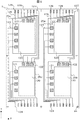
図9にOLED基板1の平面図の一例を示す。この例では、1枚のOLED基板1に4つのパネル25a〜25dが形成されている。パネル25a〜25d内部にはそれぞれ表示領域120、ゲートLSI搭載領域121、ソースLSI搭載領域122が形成されている。OLED基板1にはさらに点灯検査用のゲート部給電配線123、およびゲート部給電用電極パッド124、ソース部給電配線125、およびソース部給電用電極パッド126、第二電極給電配線127、および第二電極給電用電極パッド128が形成されている。給電プローブユニット3aはゲート部給電用電極パッド124に、給電プローブユニット3bはソース部給電用電極パッド126、および第二電極給電用電極パッド128にステージ2aの上方より触針し、給電することでOLED基板1の全画素を点灯させる。給電プローブユニット3a・3bはシステム制御部104に入力されているOLED基板情報に基づき、触針するプローブ数やプローブの触針座標を自動で設定する。給電プローブユニット3a・3bはゲート部給電用電極パッド124・ソース部給電用電極パッド126・第二電極給電用電極パッド128に触針すると、プローブ先端部に設置されたアーム(図示せず)でOLED基板1に固定される。OLED基板1はステージ2aによりX軸・Y軸方向、またはX軸方向のみに移動する。点灯検査中はOLED基板1には給電プローブユニット3a・3bがアームで固定されているため、OLED基板1が移動する際には、給電プローブユニット3a・3bも駆動部90aによりOLED基板1と同期してX軸・Y軸方向、またはX軸方向に移動する。   FIG. 9 shows an example of a plan view of the OLED substrate 1. In this example, four panels 25 a to 25 d are formed on one OLED substrate 1. A display area 120, a gate LSI mounting area 121, and a source LSI mounting area 122 are formed in the panels 25a to 25d, respectively. The OLED substrate 1 further includes a gate power supply wiring 123 for lighting inspection, a gate power supply electrode pad 124, a source power supply wiring 125, a source power supply electrode pad 126, a second electrode power supply wiring 127, and a second electrode power supply wiring 127. An electrode pad 128 for electrode feeding is formed. The feeding probe unit 3a touches the gate part feeding electrode pad 124, and the feeding probe unit 3b feeds the source part feeding electrode pad 126 and the second electrode feeding electrode pad 128 from above the stage 2a. All pixels of the OLED substrate 1 are turned on. Based on the OLED board information input to the system control unit 104, the power feeding probe units 3a and 3b automatically set the number of probes to be touched and the stylus coordinates of the probes. When the probe units 3a and 3b touch the gate portion feeding electrode pad 124, the source portion feeding electrode pad 126, and the second electrode feeding electrode pad 128, they are arms (not shown) installed at the tip of the probe. Fixed to the OLED substrate 1. The OLED substrate 1 is moved only in the X axis / Y axis direction or only in the X axis direction by the stage 2a. Since the power supply probe units 3a and 3b are fixed to the OLED substrate 1 by the arm during the lighting inspection, the power supply probe units 3a and 3b are also synchronized with the OLED substrate 1 by the drive unit 90a when the OLED substrate 1 moves. Then move in the X-axis / Y-axis direction or the X-axis direction.

OLED基板1の周辺部には、位置決め時の基準となるアライメントマーク95が複数の箇所に設けられている。   In the peripheral portion of the OLED substrate 1, alignment marks 95 serving as a reference for positioning are provided at a plurality of locations.

縮小光学系4の光学倍率は0.5倍である。カラーラインセンサ5は竹中システム機器株式会社のラインセンサカメラ:TLC-7500CLなどを使用すればよい。カラーラインセンサ5の画素数は7500、画素サイズは9.3μm×9.3μmである。OLED基板1はボトムエミッション構造であり、発光面は図5に示した構成においてガラス基板801の側であるため、ステージ2a下部には点灯検査を行うためにOLED基板の検査領域の発光の状態を観察するための切りかき20が存在する。縮小光学系4とカラーラインセンサ5はOLED基板1と切りかき20の鉛直下方向に配置され、カラーラインセンサ5の受光面は縮小光学系4に対してOLED基板1の有機発光層805と共役な位置に配置される。縮小光学系4とカラーラインセンサ5は駆動部90bにより、X軸・Y軸、またはY軸方向に移動する。縮小光学系4とカラーラインセンサ5は初期調整時、またはメンテナンス時には駆動部90bによりZ軸方向へも移動する。   The optical magnification of the reduction optical system 4 is 0.5 times. The color line sensor 5 may be a line sensor camera: TLC-7500CL manufactured by Takenaka System Equipment Co., Ltd. The color line sensor 5 has 7500 pixels and a pixel size of 9.3 μm × 9.3 μm. Since the OLED substrate 1 has a bottom emission structure and the light emitting surface is on the glass substrate 801 side in the configuration shown in FIG. 5, the state of light emission in the inspection area of the OLED substrate is shown below the stage 2a in order to perform a lighting inspection. There is a notch 20 for observation. The reduction optical system 4 and the color line sensor 5 are arranged vertically below the OLED substrate 1 and the notch 20, and the light receiving surface of the color line sensor 5 is conjugated with the organic light emitting layer 805 of the OLED substrate 1 with respect to the reduction optical system 4. It is arranged in the position. The reduction optical system 4 and the color line sensor 5 are moved in the X-axis / Y-axis or Y-axis direction by the driving unit 90b. The reduction optical system 4 and the color line sensor 5 are also moved in the Z-axis direction by the drive unit 90b during initial adjustment or maintenance.

図10A及びBと図11A及びBを用いてOLED基板1のスキャン方法の説明を行う。
図10A及びBの場合では、ステージ2aのOLED基板1を搭載する領域には長方形の切りかき20aが存在する。図10Aは正面図、図10Bは平面図を示す。図10Bに示すように、切りかき20aの大きさは例えばX軸方向に200mm、Y軸方向に300mmである。ステージ2aでOLED基板1を保持したまま、縮小光学系4とカラーラインセンサ5を駆動部90bによりX軸・Y軸方向に移動させることで、図10Aに示すようにステージ2aの切りかき20aを通してOLED基板1をスキャンし、非点灯画素を検出する。
ステージ2aの切り欠き20aを通して検査できる領域の検査を終了すると、次にOLED基板1の未スキャン領域が切りかき20aを通して検査できるようにステージ2a上でOLED基板1を移動させる。これを繰り返して、OLED基板1の全面をスキャンする。点灯検査時には給電プローブユニット3a・3bはOLED基板1にアームで固定されたまま移動するが、移動回数が多いとアームがずれる、または外れてOLED基板1が破損する恐れがあるため、OLED基板1と給電プローブユニット3a・3bの移動回数は少ないことが望ましい。上述のように、縮小光学系4とカラーラインセンサ5を主に移動させてOLED基板1をスキャンすることで、OLED基板1と給電プローブユニット3a・3bの移動回数を少なくすることが可能である。
The scanning method of the OLED substrate 1 will be described with reference to FIGS. 10A and 10B and FIGS. 11A and 11B.
In the case of FIG. 10A and B, the rectangular notch 20a exists in the area | region which mounts the OLED board | substrate 1 of the stage 2a. FIG. 10A is a front view, and FIG. 10B is a plan view. As shown in FIG. 10B, the size of the notch 20a is, for example, 200 mm in the X-axis direction and 300 mm in the Y-axis direction. While the OLED substrate 1 is held by the stage 2a, the reduction optical system 4 and the color line sensor 5 are moved in the X-axis / Y-axis directions by the driving unit 90b, thereby passing through the notch 20a of the stage 2a as shown in FIG. 10A. The OLED substrate 1 is scanned to detect non-lighting pixels.
When the inspection of the region that can be inspected through the notch 20a of the stage 2a is completed, the OLED substrate 1 is moved on the stage 2a so that the unscanned region of the OLED substrate 1 can be inspected through the notch 20a. By repeating this, the entire surface of the OLED substrate 1 is scanned. At the time of lighting inspection, the power supply probe units 3a and 3b move while being fixed to the OLED substrate 1 with an arm. It is desirable that the number of movements of the feeding probe units 3a and 3b is small. As described above, by mainly moving the reduction optical system 4 and the color line sensor 5 to scan the OLED substrate 1, it is possible to reduce the number of times the OLED substrate 1 and the power feeding probe units 3a and 3b are moved. .

図11A及びBの場合では、ステージ2aにはスリット状の切りかき20bが存在する。図11Aは正面図、図11Bは平面図を示す。切りかき20bの大きさは図11Bに示すようにX軸方向に20mm、Y軸方向にOLED基板1のY軸方向の寸法1500mmよりも大きい1700mmである。OLED基板1はステージ2a 上で駆動されてX軸方向に移動し、縮小レンズ4とカラーラインセンサ5は駆動部90bで駆動されてY軸方向に移動する。OLED基板1と縮小レンズ4・カラーラインセンサ5を互いに直交する方向に移動させることで、OLED基板1の全面をスキャンすることができる。図10A及びBの場合ではOLED基板1をX軸方向・Y軸方向に移動させる必要があるため、ステージ2aの面積が広くなるが、図11A及びBの場合ではOLED基板1の移動方向はX軸方向だけであるため、ステージ2aの面積を狭くすることができる。つまり装置のフットプリントを縮小させることができる。   In the case of FIGS. 11A and 11B, the stage 2a has a slit-shaped notch 20b. FIG. 11A is a front view, and FIG. 11B is a plan view. As shown in FIG. 11B, the size of the notch 20b is 20 mm in the X-axis direction and 1700 mm in the Y-axis direction, which is larger than the dimension 1500 mm in the Y-axis direction of the OLED substrate 1. The OLED substrate 1 is driven on the stage 2a to move in the X-axis direction, and the reduction lens 4 and the color line sensor 5 are driven by the driving unit 90b to move in the Y-axis direction. By moving the OLED substrate 1 and the reduction lens 4 / color line sensor 5 in directions orthogonal to each other, the entire surface of the OLED substrate 1 can be scanned. 10A and 10B, it is necessary to move the OLED substrate 1 in the X-axis direction and the Y-axis direction, so that the area of the stage 2a is widened. In the case of FIGS. 11A and 11B, the movement direction of the OLED substrate 1 is X Since only the axial direction is provided, the area of the stage 2a can be reduced. That is, the footprint of the apparatus can be reduced.

図12を用いて、点灯検査部101の動作フローの説明を行う。
OLED基板1が点灯検査部101にロードされると(S130)、アライメントが行われる(S131)。カラーラインセンサ5でOLED基板1に刻まれた複数のアライメント用パターン95の画像を検出し、検出画像より求められたアライメント用パターン95の座標を基にアライメントを行う。給電プローブユニット3a・3bを駆動部90aにより移動させ、ゲート部給電用電極パッド124・ソース部給電用電極パッド126・第二電極給電用電極パッド128給電パッドに触針させてOLED基板1に給電を行い、全画素を点灯させる(S132)。OLED基板1と縮小光学系4・カラーラインセンサ5を移動させることでOLED基板1をスキャンし(S133)、OLED基板1の画像を取得する。検出された画像に対して、あらかじめ定められた閾値処理を行うことで非点灯画素の検出を行う(S134)。
The operation flow of the lighting inspection unit 101 will be described with reference to FIG.
When the OLED substrate 1 is loaded on the lighting inspection unit 101 (S130), alignment is performed (S131). An image of a plurality of alignment patterns 95 carved on the OLED substrate 1 is detected by the color line sensor 5, and alignment is performed based on the coordinates of the alignment patterns 95 obtained from the detected images. The power supply probe units 3a and 3b are moved by the drive unit 90a, and the power supply electrode pad 124, the source part power supply electrode pad 126, the second electrode power supply electrode pad 128 and the second electrode power supply electrode pad 128 are touched to supply power to the OLED substrate 1. To turn on all pixels (S132). The OLED substrate 1 and the reduction optical system 4 / color line sensor 5 are moved to scan the OLED substrate 1 (S133) and acquire an image of the OLED substrate 1. A non-lighted pixel is detected by performing a predetermined threshold process on the detected image (S134).

図13は点灯検査結果の一例である。OLED基板1内でパネル25a〜25dが形成されており、それぞれのパネル内での非点灯画素26を表示している。この時、パネル毎に点灯検査を行っても、4つのパネルを同時に検査しても構わない。点灯検査部101と検査修正部102ではシステム制御部104を介して座標を共有しており、点灯検査部101で検出された非点灯画素26の座標は検査修正部102において非点灯画素26の内部に存在する欠陥の位置を特定する際に使用される。ここで欠陥とは、プロセス中の発塵などにより、図1や図2に示す透明電極と金属電極の間に異物が混入し、電極間ショートの要因となっているものを指す。   FIG. 13 is an example of a lighting inspection result. Panels 25a to 25d are formed in the OLED substrate 1, and the non-lighted pixels 26 in each panel are displayed. At this time, the lighting inspection may be performed for each panel, or four panels may be inspected simultaneously. The lighting inspection unit 101 and the inspection correction unit 102 share the coordinates via the system control unit 104, and the coordinates of the non-lighting pixels 26 detected by the lighting inspection unit 101 are stored in the non-lighting pixels 26 in the inspection correction unit 102. This is used to specify the position of a defect existing in Here, the defect refers to a defect that causes a short circuit between the electrodes due to foreign matter mixed between the transparent electrode and the metal electrode shown in FIGS. 1 and 2 due to dust generation during the process.

システム制御部104では点灯検査部101の結果に基づき検出された欠陥の数が予め設定した規定値Aよりも多いか否かの判定が行われる(S135)。非点灯画素が複数あった場合には、そのパネルの検査修正により多くの時間がかかることになる。例えばラインタクトが300秒、非点灯画素あたりの検査修正時間が5秒であれば、規定値Aとして非点灯画素数を60に設定し、非点灯画素数が60個以下のときに検査修正を行い、非点灯画素が61個以上の場合にはラインタクト内に処理できないため、そのパネルは破棄される。   The system control unit 104 determines whether or not the number of defects detected based on the result of the lighting inspection unit 101 is greater than a preset specified value A (S135). If there are a plurality of non-illuminated pixels, it takes more time to inspect and correct the panel. For example, if the line tact is 300 seconds and the inspection correction time per non-illuminated pixel is 5 seconds, the number of non-illuminated pixels is set to 60 as the specified value A, and the inspection correction is performed when the number of non-illuminated pixels is 60 or less. If the number of non-illuminated pixels is 61 or more, the panel cannot be processed in the line tact, and the panel is discarded.

以上のように非点灯画素数がラインタクト・検査修正時間に基づき計算される規定値A以上である場合には、そのパネルは不良パネルとして破棄され、修正可能なパネルのみが以後の処理を受ける。非点灯画素数が60個以下と判断されたOLED基板のうちで、非点灯画素が少なく、例えばパネルあたり5個以下であれば修正を行わなくても、そのまま製品として使用できる。そこで、次に非点灯画素が規定値B以上であるか否かを判定し(S136)、非点灯画素が規定値Bよりも少なければ、検査修正を行わずに、次の製造工程に移行し、B以上のOLED基板1はローダ103により検査修正部102へと搬送される。   As described above, when the number of non-lighted pixels is equal to or greater than the specified value A calculated based on the line tact / inspection correction time, the panel is discarded as a defective panel, and only the panel that can be corrected undergoes the subsequent processing. . Of the OLED substrates whose number of non-lighted pixels is determined to be 60 or less, the number of non-lighted pixels is small. For example, if the number is 5 or less per panel, it can be used as a product without modification. Accordingly, it is next determined whether or not the non-lighted pixels are equal to or greater than the specified value B (S136). If the number of non-lighted pixels is less than the specified value B, the process proceeds to the next manufacturing process without performing inspection correction. , B or more OLED substrates 1 are conveyed to the inspection correction unit 102 by the loader 103.

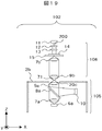
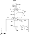
図8を用いて欠陥検査部105と修正部106の概略構成を説明する。欠陥検査部105はエリアセンサ6a、結像レンズ7a、ハーフミラー8a、対物レンズ9a、ランプ10、駆動部90cより構成され、修正部106は、光源11、エキスパンダ12、ホモジナイザ13、マスク14、マスクステージ15、結像レンズ7b・7c、ハーフミラー8b、対物レンズ9b、エリアセンサ6b、駆動部90dを備えて構成される。   A schematic configuration of the defect inspection unit 105 and the correction unit 106 will be described with reference to FIG. The defect inspection unit 105 includes an area sensor 6a, an imaging lens 7a, a half mirror 8a, an objective lens 9a, a lamp 10, and a drive unit 90c. A correction unit 106 includes a light source 11, an expander 12, a homogenizer 13, a mask 14, It comprises a mask stage 15, imaging lenses 7b and 7c, a half mirror 8b, an objective lens 9b, an area sensor 6b, and a drive unit 90d.

ステージ2bはエア浮上方式のステージであり、X軸・Y軸方向にOLED基板1を移動させる。また、ステージ2b下部にはステージ2aと同様に切りかき20cが存在し、欠陥検出部105は切りかき20cを通過し、OLED基板1の鉛直下方向に配置され、修正部106はOLED基板1の鉛直上方向に配置される。欠陥検出部105の光軸と修正部106の光軸は概略一致しており、かつ焦点位置がOLED基板1の有機発光層で概略一致している。エリアセンサ6a・6b・マスク14はOLED基板1の有機発光層と共役な位置に配置されている。後述するが、ハーフミラー8bは欠陥検出部105と修正部106の光軸と焦点位置を一致させるための初期調整時、または定期メンテナンスの時のみ配置すればよい。   The stage 2b is an air levitation type stage, and moves the OLED substrate 1 in the X-axis and Y-axis directions. In addition, a notch 20c exists at the lower part of the stage 2b, the defect detection unit 105 passes through the notch 20c, and is disposed vertically downward of the OLED substrate 1, and the correction unit 106 is provided on the OLED substrate 1. It is arranged vertically upward. The optical axis of the defect detection unit 105 and the optical axis of the correction unit 106 are approximately the same, and the focal position is approximately the same in the organic light emitting layer of the OLED substrate 1. The area sensors 6 a, 6 b, and mask 14 are disposed at positions conjugate with the organic light emitting layer of the OLED substrate 1. As will be described later, the half mirror 8b may be arranged only at the time of initial adjustment for making the optical axis and the focus position of the defect detection unit 105 and the correction unit 106 coincide with each other or at the time of regular maintenance.

欠陥検査部105は駆動部90cにより、修正部106は駆動部90dによりX軸・Y軸・Z軸方向に移動を行う。この時、欠陥検査部105と修正部106との光軸・焦点位置とを一致させるように、駆動部90c・90dは同期して欠陥検査部105と修正部106を移動させる。この時、欠陥検査部105と修正部106はオープンループ制御で移動しても、レーザ変位計(図示せず)で変位を測定しながらクローズドループ制御で移動しても構わない。また、レーザ変位計での測定の結果、光軸のずれが発生した場合には、そのずれ量だけフィードバックして移動させればよい。例えば、欠陥検査部105の光軸が修正部106の光軸に対して、X軸方向に「+1μm」だけずれていれば、欠陥検査部105の移動座標に「-1μm」だけ補正を加えて移動させればよい。   The defect inspection unit 105 is moved in the X-axis, Y-axis, and Z-axis directions by the drive unit 90c, and the correction unit 106 is moved by the drive unit 90d. At this time, the drive units 90c and 90d move the defect inspection unit 105 and the correction unit 106 in synchronization so that the optical axes and focal positions of the defect inspection unit 105 and the correction unit 106 coincide with each other. At this time, the defect inspection unit 105 and the correction unit 106 may move by open loop control, or may move by closed loop control while measuring displacement by a laser displacement meter (not shown). Further, when a deviation of the optical axis occurs as a result of the measurement by the laser displacement meter, it is only necessary to feed back and move the deviation amount. For example, if the optical axis of the defect inspection unit 105 is deviated by “+1 μm” in the X-axis direction with respect to the optical axis of the correction unit 106, the movement coordinate of the defect inspection unit 105 is corrected by “−1 μm”. And move it.

エリアセンサ6a・6bにはソニーのカラーCCDカメラ:XCL-5005CRなどを使用すればよい。画素数は2448×2050、画素サイズは3.45μm×3.45μmである。対物レンズ9aのNAは0.9であり、光学倍率は100倍である。ランプ10はハロゲンランプである。   For the area sensors 6a and 6b, a Sony color CCD camera: XCL-5005CR or the like may be used. The number of pixels is 2448 × 2050, and the pixel size is 3.45 μm × 3.45 μm. The NA of the objective lens 9a is 0.9, and the optical magnification is 100 times. The lamp 10 is a halogen lamp.

光源11はパルス発振レーザであり、波長は532nm、パルス幅は10nsである。対物レンズ9bのNAは0.4、光学倍率は50倍である。光源11より照射されたレーザ光線200はエキスパンダ12で拡大され、ホモジナイザ13で概略均一な強度分布に変換され、マスク14に照射される。マスク14に照射された時点で、レーザ光線200の直径は3mmである。結像レンズ7bと対物レンズ9bを介して、マスク14に刻まれたパターンをOLED基板1に縮小投影する。マスクステージ15の駆動方向はX軸・Y軸方向であり、マスク14をX軸・Y軸方向に移動させる。マスク14には円形・リング形状などの異なる形状・大きさの開口が存在し、マスクステージ15によりマスク14を移動させることで、OLED基板1に縮小投影させる像の形状や大きさを変更することができる。例えば、θ0.3μm程度の大きさの欠陥の場合は、外径250μm・内径150μmのリング状の開口を選択し、OLED基板1の非点灯画素26に外径5μm・内径3μm程度のリング状の加工をし、θ2μm程度の大きさの欠陥の場合は、外径500μm・内径400μmのリング状の開口を選択し、OLED基板1の非点灯画素26に外径10μm・内径8μm程度のリング状の加工を行う。   The light source 11 is a pulsed laser having a wavelength of 532 nm and a pulse width of 10 ns. The NA of the objective lens 9b is 0.4, and the optical magnification is 50 times. The laser beam 200 irradiated from the light source 11 is expanded by the expander 12, converted to a substantially uniform intensity distribution by the homogenizer 13, and irradiated to the mask 14. When the mask 14 is irradiated, the diameter of the laser beam 200 is 3 mm. The pattern carved in the mask 14 is reduced and projected onto the OLED substrate 1 through the imaging lens 7b and the objective lens 9b. The driving direction of the mask stage 15 is the X axis / Y axis direction, and the mask 14 is moved in the X axis / Y axis direction. The mask 14 has openings having different shapes and sizes such as a circular shape and a ring shape, and the shape and size of the image to be reduced and projected on the OLED substrate 1 can be changed by moving the mask 14 by the mask stage 15. Can do. For example, in the case of a defect having a size of about .theta.0.3 .mu.m, a ring-shaped opening having an outer diameter of 250 .mu.m and an inner diameter of 150 .mu.m is selected. In the case of a defect having a size of about θ2 μm, a ring-shaped opening having an outer diameter of 500 μm and an inner diameter of 400 μm is selected, and a ring-shaped opening having an outer diameter of about 10 μm and an inner diameter of about 8 μm is selected for the non-lighting pixel 26 of the OLED substrate 1. Processing.

図14を用いて非点灯画素26にレーザ照射を行い、非点灯画素26が加工された時の状態の一例を説明する。図14(a)はレーザ照射前の非点灯画素26に存在する欠陥30を欠陥検査部105から観察した画像、(b)はレーザ照射前のOLED基板1の欠陥30を含む部位の断面、(c)はレーザ照射後の非点灯画素26に存在する欠陥30を欠陥検査部105から観察した画像、及び(d)はレーザ照射後のOLED基板1の欠陥30を含む部位の断面を示している。   An example of the state when the non-lighting pixel 26 is processed by irradiating the non-lighting pixel 26 with laser will be described with reference to FIG. 14A is an image obtained by observing the defect 30 existing in the non-lighted pixel 26 before the laser irradiation from the defect inspection unit 105, and FIG. 14B is a cross-section of a portion including the defect 30 of the OLED substrate 1 before the laser irradiation. c) shows an image obtained by observing the defect 30 existing in the non-illuminated pixel 26 after the laser irradiation from the defect inspection unit 105, and (d) shows a cross section of a portion including the defect 30 of the OLED substrate 1 after the laser irradiation. .

図14(a)に示すように、欠陥30が欠陥検査部105の視野31の中心に位置している。修正部106と欠陥検査部105の光軸と焦点位置を概略一致させているため、欠陥検査部105の視野中心に欠陥30を移動させれば、修正部106の視野中心に欠陥30は位置することになる。非点灯画素26に縮小投影するマスク14の開口は外径250μm・内径150μmのリング形状であり、照射エネルギは0.1mJ/パルスである。上記照明条件でレーザを1パルス照射すると、図14(c)に示すように、非点灯画素26には外径5μm・内径3μm程度の加工跡33が形成される。レーザ照射によって欠陥30存在部位は加工されず、パルスレーザ照射による衝撃波で図14(d)に示すように異物30の真上の部分の金属電極803がリング状に加工される。レーザの照射エネルギ密度を適切に設定することにより有機発光層804がレーザストッパ層となり、加工は、最上層の金属電極803の層だけになる。これにより、欠陥30と接触している部分の金属電極803を周囲から孤立化させることができるため、欠陥30による電極間ショートが解消され、画素が救済される。欠陥30自体は加工されないため、飛散した欠陥が別の欠陥要因となることを避けることができる。   As shown in FIG. 14A, the defect 30 is located at the center of the visual field 31 of the defect inspection unit 105. Since the optical axis and the focal position of the correction unit 106 and the defect inspection unit 105 are approximately matched, if the defect 30 is moved to the center of the visual field of the defect inspection unit 105, the defect 30 is positioned at the visual field center of the correction unit 106. It will be. The opening of the mask 14 to be reduced and projected onto the non-lighted pixels 26 has a ring shape with an outer diameter of 250 μm and an inner diameter of 150 μm, and the irradiation energy is 0.1 mJ / pulse. When one pulse of laser is irradiated under the above illumination conditions, as shown in FIG. 14C, a processing trace 33 having an outer diameter of about 5 μm and an inner diameter of about 3 μm is formed in the non-lighting pixel 26. The portion where the defect 30 is present is not processed by the laser irradiation, and the metal electrode 803 immediately above the foreign material 30 is processed into a ring shape by a shock wave generated by the pulse laser irradiation as shown in FIG. By appropriately setting the irradiation energy density of the laser, the organic light emitting layer 804 becomes a laser stopper layer, and only the uppermost metal electrode 803 is processed. As a result, the metal electrode 803 that is in contact with the defect 30 can be isolated from the surroundings, so that the short circuit between the electrodes due to the defect 30 is eliminated and the pixel is relieved. Since the defect 30 itself is not processed, it can be avoided that the scattered defect becomes another defect factor.

図15を用いて非点灯画素26にレーザ照射を行い、非点灯画素26が加工する別の例を説明する。図15(a)はレーザ照射前の非点灯画素26に存在する欠陥30を欠陥検査部105から観察した画像、(b)はレーザ照射前のOLED基板1の欠陥30を含む部位の断面、(c)はレーザ照射後の非点灯画素26に存在する欠陥30を欠陥検査部105から観察した画像、及び(d)はレーザ照射後のOLED基板1の断面を示している。   Another example in which the non-lighted pixels 26 are processed by irradiating the non-lighted pixels 26 with laser will be described with reference to FIG. 15A is an image obtained by observing the defect 30 existing in the non-lighted pixel 26 before laser irradiation from the defect inspection unit 105, and FIG. 15B is a cross-section of a portion including the defect 30 of the OLED substrate 1 before laser irradiation. c) shows an image obtained by observing the defect 30 existing in the non-illuminated pixel 26 after the laser irradiation from the defect inspection unit 105, and (d) shows a cross section of the OLED substrate 1 after the laser irradiation.

図15(a)は、欠陥30が欠陥検査部105の視野31の中心に位置している状態を観察した画像である。修正部106と欠陥検査部105の光軸と焦点位置を概略一致させているため、欠陥検査部105の視野中心に欠陥30を移動させれば、修正部106の視野中心に欠陥30は位置することになる。非点灯画素26に縮小投影するマスク14の開口は?150μmの円形状であり、照射エネルギは0.1mJ/パルスである。上記照明条件でレーザを1パルス照射すると、非点灯画素26には図15(c)に示すように?3μm程度の加工跡35が形成される。レーザ照射によって、図15(b)に示すような金属電極803の欠陥30の真上の部位が、レーザ照射によって図15(d)に示すように除去加工され、欠陥30による電極間ショートが解消され、画素が救済される。図15(d)のように円形状の加工をする場合には、図14(d)に示したようなリング形状の加工をする場合と比較して加工寸法を小さくすることができ、非発光面積の増大を抑制することができる。   FIG. 15A is an image obtained by observing a state in which the defect 30 is positioned at the center of the field of view 31 of the defect inspection unit 105. Since the optical axis and the focal position of the correction unit 106 and the defect inspection unit 105 are approximately matched, if the defect 30 is moved to the center of the visual field of the defect inspection unit 105, the defect 30 is positioned at the visual field center of the correction unit 106. It will be. What is the opening of the mask 14 to be reduced and projected onto the non-lighted pixel 26? It has a circular shape of 150 μm, and the irradiation energy is 0.1 mJ / pulse. When one pulse of laser is irradiated under the above illumination conditions, as shown in FIG. A processing mark 35 of about 3 μm is formed. By laser irradiation, the portion directly above the defect 30 of the metal electrode 803 as shown in FIG. 15B is removed by laser irradiation as shown in FIG. And the pixel is relieved. When circular processing is performed as shown in FIG. 15D, the processing dimensions can be reduced compared to the case of ring processing as shown in FIG. An increase in area can be suppressed.

図16は非点灯画素26に異なる二つの欠陥30・36が存在する場合を示している。欠陥30のように非点灯画素26の比較的中心部に近い場所に位置していれば、図14、図15を用いて説明したように欠陥30を欠陥検査部105の視野の中心に移動させてレーザ照射を行い、加工跡33を形成しても構わないが、欠陥36のように非点灯画素26の端にある欠陥の場合、欠陥検査部105の視野中心に欠陥36を移動させ、レーザ照射を行い加工跡37を生成しようとすると、レーザの一部が非点灯画素26から外れてしまい、画素駆動回路や配線パターン部分にダメージを与える可能性がある。   FIG. 16 shows a case where two different defects 30 and 36 exist in the non-lighted pixel 26. If the defect 30 is located at a position relatively close to the center of the non-illuminated pixel 26, the defect 30 is moved to the center of the visual field of the defect inspection unit 105 as described with reference to FIGS. However, in the case of a defect at the end of the non-illuminated pixel 26 like the defect 36, the defect 36 is moved to the center of the visual field of the defect inspection unit 105, and the laser is irradiated. If it is attempted to generate the processing trace 37 by irradiation, a part of the laser may be detached from the non-illuminated pixel 26, and there is a possibility of damaging the pixel driving circuit and the wiring pattern portion.

図17は欠陥36を欠陥検査部105から観察した画像の一例である。このような場合には、欠陥のサイズや座標から適切なマスク形状を選択し、欠陥の座標や大きさに基づき計算される距離だけ、欠陥36を欠陥検査部105の視野中心からずらした位置に移動させ、レーザ照射を行い、加工跡38を形成しても構わない。例えば、欠陥36のサイズが?0.3μmであり、画素の端から2μmだけ離れた位置に存在している場合には、視野の中心からX軸方向に+1μmだけずらした位置に欠陥36を位置させ、外径5μm、内径3μm程度のリング形状の加工跡38を形成すればよい。   FIG. 17 is an example of an image obtained by observing the defect 36 from the defect inspection unit 105. In such a case, an appropriate mask shape is selected from the size and coordinates of the defect, and the defect 36 is shifted from the center of the visual field of the defect inspection unit 105 by a distance calculated based on the coordinates and size of the defect. The processing trace 38 may be formed by moving the laser beam and performing laser irradiation. For example, what is the size of the defect 36? If it is 0.3 μm and exists at a position 2 μm away from the edge of the pixel, the defect 36 is located at a position shifted by +1 μm in the X-axis direction from the center of the field of view, and the outer diameter is 5 μm and the inner diameter is 3 μm. What is necessary is just to form the ring-shaped process trace 38 of a grade.

欠陥検査部105と修正部106の光軸と焦点を一致させるために、初期出荷時、または定期メンテナンス時には以下の調整が行われる。図18は検査修正部102のみを示している。透明OLED基板70がステージ2aに搬送され、透明OLED基板70を点灯させて、光軸と焦点の調整が行われる。一般的なOLED基板は図1、図2に示すように、透明電極と金属電極で有機発光層を挟んでおり、透明電極側から光を取り出すが、透明OLED基板70は透明電極同士で有機発光層を挟んでいるため、両方向に光を取り出すことができる。   In order to make the optical axes and the focal points of the defect inspection unit 105 and the correction unit 106 coincide with each other, the following adjustment is performed at the time of initial shipment or regular maintenance. FIG. 18 shows only the inspection correction unit 102. The transparent OLED substrate 70 is conveyed to the stage 2a, and the transparent OLED substrate 70 is turned on to adjust the optical axis and focus. As shown in FIGS. 1 and 2, a general OLED substrate has an organic light emitting layer sandwiched between a transparent electrode and a metal electrode, and light is taken out from the transparent electrode side. However, the transparent OLED substrate 70 emits organic light between the transparent electrodes. Since the layers are sandwiched, light can be extracted in both directions.

修正部106側からは、ハーフミラー8b、結像レンズ7c、エリアセンサ6bを備えた観察光学系107を介して透明OLED基板70を観察する。エリアセンサ6a・6bの画像を確認しながら、欠陥検査部105と修正部106をZ方向に移動させ、焦点位置を透明OLED基板70の有機発光層にあわせる。さらに光軸を一致させるために、欠陥検査部105と修正部106をX軸・Y軸方向に移動させ、透明OLED基板70の同一領域を検出するように調整する。この時、透明OLED基板70に大きさの異なる画素や異なる形状の画素を複数形成しておけば、欠陥検査部105と修正部106との検出領域が一致していることの確認を取りやすい。   From the correction unit 106 side, the transparent OLED substrate 70 is observed through the observation optical system 107 including the half mirror 8b, the imaging lens 7c, and the area sensor 6b. While checking the images of the area sensors 6a and 6b, the defect inspection unit 105 and the correction unit 106 are moved in the Z direction, and the focal position is adjusted to the organic light emitting layer of the transparent OLED substrate 70. Further, in order to make the optical axes coincide with each other, the defect inspection unit 105 and the correction unit 106 are moved in the X-axis / Y-axis directions and adjusted so as to detect the same region of the transparent OLED substrate 70. At this time, if a plurality of pixels having different sizes or different shapes are formed on the transparent OLED substrate 70, it is easy to confirm that the detection areas of the defect inspection unit 105 and the correction unit 106 match.

調整時には修正部106側からも画像を取得するために観察光学系107のハーフミラー8bをレーザ200の光路中に入れることが必要だが、修正時にはレーザ200の光路を遮ってしまうために、調整時以外は図示していない駆動機構を用いてレーザ200の光路からハーフミラー8bを退避させる。   At the time of adjustment, it is necessary to put the half mirror 8b of the observation optical system 107 in the optical path of the laser 200 in order to acquire an image also from the correction unit 106 side. The half mirror 8b is retracted from the optical path of the laser 200 using a drive mechanism (not shown) except for the above.

透明OLED基板70を使用しなくても、ガラス基板上にクロムなどでパターンを形成したサンプルを用いて、光軸、および焦点位置の調整を行っても構わない。   Even if the transparent OLED substrate 70 is not used, the optical axis and the focal position may be adjusted using a sample in which a pattern is formed with chromium or the like on a glass substrate.

図19に透明OLED基板70を使用しない調整方法を示す。修正部106の対物レンズ9bでレーザ光源11からエネルギを小さくして発射されたレーザ22による点像71を形成する。そして駆動部90cで欠陥検査部105をX軸・Y軸・Z軸方向に移動させて、欠陥検査部105の焦点位置を点像71の座標に合わせることで、光軸・焦点位置を一致させても構わない。この方法では、透明OLED基板70を用意する必要がなく、また、透明OLED基板70の画像を取得するためのエリアセンサ6b、結像レンズ7c、ハーフミラー8bを含む観察光学系107が必要ないため、装置構成を簡略化させることができる。   FIG. 19 shows an adjustment method that does not use the transparent OLED substrate 70. A point image 71 by the laser 22 emitted from the laser light source 11 with reduced energy is formed by the objective lens 9b of the correction unit 106. The drive unit 90c moves the defect inspection unit 105 in the X-axis / Y-axis / Z-axis directions so that the focal position of the defect inspection unit 105 matches the coordinates of the point image 71, thereby matching the optical axis / focus position. It doesn't matter. In this method, it is not necessary to prepare the transparent OLED substrate 70, and the observation optical system 107 including the area sensor 6b, the imaging lens 7c, and the half mirror 8b for acquiring an image of the transparent OLED substrate 70 is not necessary. The apparatus configuration can be simplified.

図20を用いて欠陥検査部105の動作フローの説明を行う。
欠陥検査部105のステージ2bにOLED基板1が搬送されると、OLED基板1のアライメント用パターン95を検出してOLED基板1のアライメントが行われる(S40)。この時、対物レンズ9aを光学倍率10倍、NA0.28のレンズに交換し、視野を広げる。システム制御部104の指令に基づき、非点灯画素26の周辺が欠陥検査部105の視野内に概ねはいるようにOLED基板1、および欠陥検査部105・修正部106を移動させ(S41)、対物レンズ9aをNA0.9、光学倍率100倍のレンズに交換し、ファインアライメントを行う(S42)。この時、OLED基板1と欠陥検査部105・修正部106はそれぞれがX方向・Y方向に移動しても、お互いに直交する1軸方向のみに移動しても構わない。図21はOLED基板1の平面図、および、パネル25aに存在する非点灯画素26とその周辺部の拡大図である。図21の場合では、赤(R)発光画素26が非点灯となっており、緑(G)発光画素27、青(B)発光画素28が隣接しており、正常な赤発光画素26’、緑発光画素27’、青発光画素28’が並列している。ここで、画素サイズは赤・緑・青発光画素のサイズは全て80μm×240μmである。非点灯画素26には欠陥30が存在している。
The operation flow of the defect inspection unit 105 will be described with reference to FIG.
When the OLED substrate 1 is transported to the stage 2b of the defect inspection unit 105, the alignment pattern 95 of the OLED substrate 1 is detected and the OLED substrate 1 is aligned (S40). At this time, the objective lens 9a is replaced with a lens having an optical magnification of 10 times and NA of 0.28 to widen the field of view. Based on the command from the system control unit 104, the OLED substrate 1 and the defect inspection unit 105 / correction unit 106 are moved so that the periphery of the non-illuminated pixel 26 is substantially within the field of view of the defect inspection unit 105 (S41). The lens 9a is replaced with a lens having NA of 0.9 and an optical magnification of 100, and fine alignment is performed (S42). At this time, the OLED substrate 1, the defect inspection unit 105, and the correction unit 106 may move in the X direction and the Y direction, respectively, or may move only in one axial direction orthogonal to each other. FIG. 21 is a plan view of the OLED substrate 1 and an enlarged view of the non-illuminated pixels 26 present in the panel 25a and the periphery thereof. In the case of FIG. 21, the red (R) light emitting pixel 26 is not lit, the green (G) light emitting pixel 27 and the blue (B) light emitting pixel 28 are adjacent to each other, and the normal red light emitting pixel 26 ′, A green light emitting pixel 27 ′ and a blue light emitting pixel 28 ′ are arranged in parallel. Here, the pixel sizes are all red, green, and blue light emitting pixels of 80 μm × 240 μm. The non-lighted pixel 26 has a defect 30.

非点灯画素26と同じ発光色の赤発光画素26’の画像を取得し(S43)、次に、非点灯画素26、またはその周辺部が欠陥検査部105の視野内に概ねはいるようにOLED基板1、および欠陥検査部105・修正部106を移動させ(S44)、非点灯画素26の画像を取得する(S45)。エリアセンサ6aのOLED基板1上における視野は85μm×70μm程度であるため、図21に示すように、パネル25aの1画素を4つの検出範囲29a〜29dに分けて画像取得を行い、それらをマージして、1画素分の画像を生成すればよい。非点灯画素26がマージした後の画像のおよそ中心になるように位置合わせをして4つの画像を個別に取得する。この時、非点灯画素26以外の領域の画像を取得しても構わない。   An image of the red light-emitting pixel 26 ′ having the same emission color as that of the non-lighting pixel 26 is acquired (S 43), and then the OLED so that the non-lighting pixel 26 or its peripheral part is generally within the visual field of the defect inspection unit 105. The substrate 1 and the defect inspection unit 105 / correction unit 106 are moved (S44), and an image of the non-lighted pixels 26 is acquired (S45). Since the field of view of the area sensor 6a on the OLED substrate 1 is about 85 μm × 70 μm, as shown in FIG. 21, one pixel of the panel 25a is divided into four detection ranges 29a to 29d to acquire images and merge them. Then, an image for one pixel may be generated. Four images are obtained individually by positioning so that the non-illuminated pixel 26 is approximately at the center of the merged image. At this time, an image of an area other than the non-lighted pixels 26 may be acquired.

次に、システム制御部104で、取得した非点灯画素26の画像と赤発光画素26’の画像との位置合わせを行い(S46)、差画像をとることで(S47)、欠陥30を強調することができる。差画像にあらかじめ決められた閾値処理を行い(S48)、閾値以上の輝度値であったものを欠陥として抽出する(S49)。図21の例では赤・緑・青発光画素はすべて同じ大きさであったが、赤・緑・青発光の画素によって、画素の大きさが異なる場合があるため、非点灯画素と同一発光色の画素同士の差画像を取得することが望ましい。   Next, the system control unit 104 aligns the acquired image of the non-illuminated pixel 26 and the image of the red light emitting pixel 26 '(S46), and takes the difference image (S47) to emphasize the defect 30. be able to. A predetermined threshold process is performed on the difference image (S48), and a luminance value equal to or higher than the threshold value is extracted as a defect (S49). In the example of FIG. 21, the red, green, and blue light emitting pixels are all the same size, but the pixel size may differ depending on the red, green, and blue light emitting pixels. It is desirable to obtain a difference image between the pixels.

システム制御部104では欠陥検査部105の検査結果に基づき非点灯画素26の修正可否を判定する。図22を用いて修正可否判定フローの説明を行う。   The system control unit 104 determines whether or not the non-lit pixel 26 can be corrected based on the inspection result of the defect inspection unit 105. The correction possibility determination flow will be described with reference to FIG.

先ず、非点灯画素26での欠陥の有無を確認する(S50)。即ち、S49で欠陥が抽出されたか否かを確認する。この時、欠陥が検出されなければ、TFT層形成工程における不良など、異物混入以外の要因により画素が非点灯になっているため、該当画素は修正不可能と判定する。
次に、S49で欠陥が抽出された場合には、欠陥の存在箇所を確認する(S51)。図16で説明したように、欠陥の位置によってはレーザ照射を行うと画素駆動回路や配線パターンなどの部分にレーザが当たる可能性もあり、その場合には画素駆動回路や配線パターンなどの部分にダメージが生じ、回路起因の別の欠陥が発生する可能性がある。欠陥の存在箇所を確認し、レーザ照射により回路起因の欠陥が発生する場合にも該当画素は修正不可能と判定する。
First, the presence / absence of a defect in the non-lighted pixel 26 is confirmed (S50). That is, it is confirmed whether or not a defect is extracted in S49. At this time, if no defect is detected, it is determined that the pixel cannot be corrected because the pixel is not lit due to a factor other than contamination such as a defect in the TFT layer forming process.
Next, when a defect is extracted in S49, the location of the defect is confirmed (S51). As described with reference to FIG. 16, depending on the position of the defect, there is a possibility that the laser hits a part such as a pixel driving circuit or a wiring pattern when laser irradiation is performed. Damage can occur and other defects resulting from the circuit can occur. The presence of a defect is confirmed, and even when a defect caused by a circuit occurs due to laser irradiation, it is determined that the corresponding pixel cannot be corrected.

次に、検出画像や差画像に基づき欠陥を分類し(S52)、欠陥の大きさや長さを求めるサイジングを行う(S53)。欠陥種や大きさによっては修正ができない場合も存在し、かつその欠陥が確実に致命である場合にも、該当画素は修正不可能と判定する(S54)。   Next, the defect is classified based on the detected image and the difference image (S52), and sizing for obtaining the size and length of the defect is performed (S53). Depending on the defect type and size, there is a case where the correction cannot be made, and even when the defect is definitely fatal, it is determined that the corresponding pixel cannot be corrected (S54).

非点灯画素26に複数の欠陥が存在する場合には全ての欠陥に対してレーザ照射を行うため、非点灯画素26で非発光となる面積は増大する。また、欠陥サイズが大きい場合には大きい場合には、電極間ショートを解消するために大きな形状で非点灯画素26に加工を行う必要があるため、この場合にも非発光となる面積が増大する。θ5μmの加工跡が形成された場合の非発光面積は19.6μm2であり、θ10μmの加工跡が形成された場合の非発光面積は78.5μm2である。レーザ照射により非発光となる面積の許容値を画素全体の0.5%以下と規定する場合には、画素サイズが80μm×240μmの時には、非発光面積が96μm2を超えると該当画素は修正不可と判定する。 When there are a plurality of defects in the non-lighted pixels 26, laser irradiation is performed on all the defects, so that the non-light emitting area of the non-lighted pixels 26 increases. Further, when the defect size is large, if the defect size is large, it is necessary to process the non-illuminated pixel 26 in a large shape in order to eliminate the short-circuit between electrodes, and in this case also, the area that does not emit light increases. . The non-light emitting area when the processing trace of θ5 μm is formed is 19.6 μm 2 , and the non-light emitting area when the processing trace of θ10 μm is formed is 78.5 μm 2 . When the allowable value of the non-light-emitting area by laser irradiation is specified to be 0.5% or less of the entire pixel, when the pixel size is 80 μm × 240 μm, the corresponding pixel cannot be corrected if the non-light-emitting area exceeds 96 μm 2 Is determined.

以上のように、非発光となる面積は、一定値以下に抑える必要があるため、レーザ照射により画素内の非発光となる面積が規定値C以上である場合にも、該当画素の修正は不可能と判定する(S55)。   As described above, it is necessary to suppress the non-light-emitting area to a certain value or less. Therefore, even when the non-light-emitting area in the pixel by laser irradiation is equal to or greater than the specified value C, the correction of the corresponding pixel is not possible. It is determined that it is possible (S55).

上記修正可否判定フローにより、該当画素は修正可能と判定された場合に、次に示す修正工程にうつる(S56)。   If it is determined by the correction possibility determination flow that the pixel can be corrected, the correction process shown below is performed (S56).

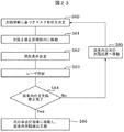
図23を用いて修正部106の動作フローの説明を行う。
欠陥30の座標や大きさなどの情報に基づきマスク14の形状・大きさを決定する(S60)。欠陥30を欠陥検査部105の視野中心に移動させる(S61)。照射エネルギなどの照明条件を決定し(S62)、レーザ照射を行う(S63)。例えば、マスク14の形状が外径250μm・内径150μmのリング形状であれば0.1mJ/パルスの照射エネルギでレーザ照明を行い、マスク14の形状が外径500μm・内径400μmのリング形状であれば0.2mJ/パルスの照射エネルギでレーザ照明を行う。マスク14の非開口部や結像レンズ7b・対物レンズ9bの透過率により照射エネルギのロスが発生するが、非点灯画素26面での照射エネルギ密度が2.0J/cm2〜10.0J/cm2の範囲となるように照射エネルギを調整する。画素内に欠陥が複数あった場合には、全ての欠陥の修正を行ったか判定し(S64)、修正していない欠陥があれば、別の欠陥に対して「S60〜63」を再度行う(S65)。全ての欠陥が修正完了していれば、次の非点灯画素に対して検査修正を行う(S66)。
The operation flow of the correction unit 106 will be described with reference to FIG.
The shape / size of the mask 14 is determined based on information such as the coordinates and size of the defect 30 (S60). The defect 30 is moved to the center of the visual field of the defect inspection unit 105 (S61). Illumination conditions such as irradiation energy are determined (S62), and laser irradiation is performed (S63). For example, if the mask 14 has a ring shape with an outer diameter of 250 μm and an inner diameter of 150 μm, laser illumination is performed with an irradiation energy of 0.1 mJ / pulse, and if the mask 14 has a ring shape with an outer diameter of 500 μm and an inner diameter of 400 μm. Laser illumination is performed with an irradiation energy of 0.2 mJ / pulse. Irradiation energy loss occurs due to the non-aperture of the mask 14 and the transmittance of the imaging lens 7b and the objective lens 9b, but the irradiation energy density on the non-illuminated pixel 26 surface is 2.0 J / cm 2 to 10.0 J /. adjusting the irradiation energy to be in the range of cm 2. If there are a plurality of defects in the pixel, it is determined whether all the defects have been corrected (S64). If there is an uncorrected defect, "S60 to 63" is performed again for another defect ( S65). If all the defects have been corrected, inspection correction is performed on the next non-lighted pixel (S66).

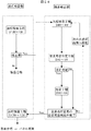
以上、点灯検査部101での動作フロー(図12)、欠陥検出部105での動作フロー(図20)、非点灯画素の修正可否判定フロー(図22)、修正部106の動作フロー(図23)の説明を行った。図24を用いて検査修正装置全体の動作フローの説明を行う。   The operation flow in the lighting inspection unit 101 (FIG. 12), the operation flow in the defect detection unit 105 (FIG. 20), the non-lighting pixel correction possibility determination flow (FIG. 22), and the operation flow in the correction unit 106 (FIG. 23). ) Was explained. The operation flow of the entire inspection / correction apparatus will be described with reference to FIG.

点灯検査部101において、図12で説明したOLED基板1の点灯検査、ならびにOLED基板1の修正可否判定などの点灯検査工程S130〜136が実施される。S136で修正要と判定されたOLED基板1はローダ103を経由して検査修正部102に搬送され、図20で説明したファインアライメント、ならびに欠陥検出などの欠陥検査工程S40〜49が実施される。システム制御部104では、欠陥検査部105の検査結果に基づき、図22で説明した修正可否判定工程S50〜56が実施されて非点灯画素26の修正可否判定が行われる。S55で修正可能と判断された非点灯画素26に対しては、検査修正部102の修正部106において、図23で説明した修正工程S60〜66に記載の修正工程が実施される。   In the lighting inspection unit 101, lighting inspection steps S130 to S136 such as the lighting inspection of the OLED substrate 1 described in FIG. The OLED substrate 1 determined to be corrected in S136 is transported to the inspection correction unit 102 via the loader 103, and the defect inspection steps S40 to S49 such as fine alignment and defect detection described in FIG. 20 are performed. In the system control unit 104, based on the inspection result of the defect inspection unit 105, the correction possibility determination steps S50 to S56 described with reference to FIG. For the non-lighted pixels 26 determined to be correctable in S55, the correction process described in the correction processes S60 to 66 described in FIG. 23 is performed in the correction unit 106 of the inspection correction unit 102.

全ての非点灯画素26の修正可否判定が終了すれば、OLED基板1は再度点灯検査部101に搬送され、図12で説明した点灯検査工程S130〜136に記載の点灯検査工程が実施され、修正工程を経たパネルの非点灯画素数が規定値Aよりも多い場合にはパネル破棄、非点灯画素数が規定値Bよりも少なくなった場合には製品として合格の判定が下される。修正工程を経たパネルの非点灯画素数が規定値A以下で規定値B以上の場合には、ラインから抜き取って再度検査修正工程を繰り返すかを検査員が判定する。この段階でパネル破棄と判定されても、ラインタクトに余裕があれば再度検査修正工程を繰り返すこともできる。   When the determination of whether or not all the non-lighting pixels 26 can be corrected is completed, the OLED substrate 1 is transported again to the lighting inspection unit 101, and the lighting inspection process described in the lighting inspection processes S130 to 136 described with reference to FIG. When the number of non-lighted pixels of the panel that has undergone the process is larger than the prescribed value A, the panel is discarded, and when the number of non-lighted pixels is smaller than the prescribed value B, the product is judged to pass. If the number of non-lighted pixels of the panel that has undergone the correction process is equal to or less than the specified value A and equal to or greater than the specified value B, the inspector determines whether to extract the line from the line and repeat the inspection correction process again. Even if it is determined that the panel is discarded at this stage, the inspection correction process can be repeated if the line tact has a margin.

本実施例では、OLED基板1が樹脂・ガラス封止される前の工程で検査修正が行われる一例で説明を行ったが、OLED製造工程のどの工程で検査修正を行っても良い。例えば、樹脂・ガラス封止をし、パネル毎に切断された後で検査修正を行っても良い。この場合、取り扱い基板の大きさが小さくなるため、装置のフットプリントを小さくすることができる。ただし、この場合には、欠陥箇所の上に存在する樹脂やガラス基板を部分的に除去する為の手段(例えば、FIB(Focused Ion Beam)加工装置)及び、欠陥箇所を処理後に上記部分的に除去した樹脂やガラス基板の部分に樹脂やガラス基板に相当する物質を充填するための手段(例えば、レーザCVD(Chemical Vapor Deposition)装置)などが必要になる。   In the present embodiment, an example in which inspection and correction are performed in a process before the OLED substrate 1 is sealed with resin and glass has been described, but the inspection and correction may be performed in any process of the OLED manufacturing process. For example, resin / glass sealing may be performed, and inspection correction may be performed after being cut for each panel. In this case, since the size of the handling substrate is reduced, the footprint of the apparatus can be reduced. However, in this case, a means (for example, a FIB (Focused Ion Beam) processing apparatus) for partially removing the resin or glass substrate existing on the defective portion and the above-mentioned partial portion after processing the defective portion. Means (for example, a laser CVD (Chemical Vapor Deposition) apparatus) for filling the removed resin or glass substrate with a material corresponding to the resin or glass substrate is required.

また、樹脂・ガラス封止工程前で検査修正を行う場合には、レーザ照射部にHeガスなどのアシストガスをふきつけて、溶融飛散物の飛散を抑制することもできる。または、レーザ照射部近傍にピペットを配置して、溶融飛散物を吸引することもできる。溶融飛散物が周囲へ飛散することで新たな欠陥が発生する可能性があるため、アシストガスで飛散物の量を抑制する、またはピペットで飛散物を吸引することで、新たな欠陥発生の確率を低くすることができる。   In addition, when inspection and correction are performed before the resin / glass sealing step, it is possible to suppress the scattering of the molten scattered matter by wiping the laser irradiation portion with an assist gas such as He gas. Or a pipette can be arrange | positioned in the laser irradiation part vicinity, and a molten scattered matter can also be attracted | sucked. Since new flaws may occur when the molten scattered material scatters to the surroundings, the probability of new flaws occurring when the amount of the scattered material is reduced with an assist gas or the scattered material is sucked with a pipette. Can be lowered.

本実施例では、点灯検査部101と検査修正部102が同一筐体内にある例で説明を行ったが、別々の筐体にあっても構わない。ライン立ち上げ時には製造プロセスが安定しておらず、OLEDパネル1への異物混入の頻度も高く、修正を行う頻度が高くなる。タクト短縮のためには点灯検査部101から検査修正部102へのOLED基板1の搬送時間を短くする必要があり、このような場合では点灯検査部101と検査修正部102が同一筐体内に存在するほうが有効である。   In this embodiment, the lighting inspection unit 101 and the inspection correction unit 102 are described as being in the same casing, but they may be in separate casings. When the line is started up, the manufacturing process is not stable, the frequency of contamination of the OLED panel 1 is high, and the frequency of correction is high. In order to shorten the tact time, it is necessary to shorten the transport time of the OLED substrate 1 from the lighting inspection unit 101 to the inspection correction unit 102. In such a case, the lighting inspection unit 101 and the inspection correction unit 102 exist in the same housing. It is more effective to do this.

一方、製造プロセスが成熟すると装置発塵の頻度も減り、点灯検査の結果、非点灯画素が規定値B以下となり、修正が不要となるケースが増加する。つまり、点灯検査部101から検査修正部102へOLED基板1を搬送する頻度が少なくなり、点灯検査部101と検査修正部102が同一の筐体に存在する必要性が低くなる。樹脂封止工程前に検査修正を行う場合には装置内部をドライ窒素で満たしているため、点灯検査部101と検査修正部102を別々の筐体に分けて、装置を小型化するほうがランニングコスト低減に効果がある。   On the other hand, when the manufacturing process matures, the frequency of device dust generation also decreases, and as a result of lighting inspection, non-lighting pixels become less than the prescribed value B, and the number of cases where correction is unnecessary increases. That is, the frequency with which the OLED substrate 1 is transported from the lighting inspection unit 101 to the inspection correction unit 102 is reduced, and the necessity of the lighting inspection unit 101 and the inspection correction unit 102 being in the same casing is reduced. When the inspection correction is performed before the resin sealing process, since the inside of the apparatus is filled with dry nitrogen, it is more costly to divide the lighting inspection unit 101 and the inspection correction unit 102 into separate housings and downsize the apparatus. It is effective for reduction.

本実施例では、検査修正部102で検査修正後の点灯検査は点灯検査部101にOLED基板1を再度搬送して、点灯検査部101において行う例で説明したが、検査修正部102で点灯検査を行っても構わない。この場合、検査修正部102内にも給電プローブユニットを配備し、検査修正中も全画素を常に点灯させておく。修正により画素が救済されれば、修正が完了した時点で発光するようになるため、欠陥検査部105のエリアセンサ6aで点灯の有無を確認することができる。システム制御部104では、点灯検査部101で点灯検査により検出された非点灯画素の数と、検査修正部102において救済された画素の数を記録しておき、最終的な非点灯画素の数をカウントする。これが規定値Bと比較し、規定値B以上であれば、不良パネルとして破棄と判定する。検査修正部102において、点灯検査を行えばOLED基板1の搬送を省略することができるため、ラインタクトを短縮することが可能である。   In the present embodiment, the lighting inspection after the inspection correction by the inspection correction unit 102 has been described as an example in which the OLED substrate 1 is transported again to the lighting inspection unit 101 and performed in the lighting inspection unit 101. You may do. In this case, a power supply probe unit is also provided in the inspection correction unit 102, and all pixels are always lit even during inspection correction. If the pixel is relieved by the correction, light is emitted when the correction is completed. Therefore, the area sensor 6a of the defect inspection unit 105 can check whether or not the pixel is lit. The system control unit 104 records the number of non-lit pixels detected by the lighting test unit 101 by the lighting test and the number of pixels relieved by the test correction unit 102, and determines the final number of non-lit pixels. Count. If this is compared with the prescribed value B and if it is equal to or greater than the prescribed value B, it is determined to be discarded as a defective panel. In the inspection correcting unit 102, if the lighting inspection is performed, the conveyance of the OLED substrate 1 can be omitted, so that the line tact can be shortened.

図25A及びBに、本実施例で説明した検査修正装置で検査した結果を出力する画面の一例を示す。   FIGS. 25A and 25B show an example of a screen for outputting the result of inspection by the inspection correction apparatus described in the present embodiment.

図25Aには、あるOLED基板を検査した結果を表示する例を示す。画面2500には、OLED基板であるマザーガラスのID番号2501、OLED基板内のパネル番号2502、そのパネル内で検出された非点灯画素数2503、本検査修正装置で処理した結果修正が成功した数2504、修正対象外となった非修正画素数2505、最終的な非点灯画素数2506、パネルとしての最終的な合否判定の結果2507を表示する。   FIG. 25A shows an example of displaying the result of inspecting a certain OLED substrate. On the screen 2500, there is an ID number 2501 of the mother glass as the OLED substrate, a panel number 2502 in the OLED substrate, the number of non-illuminated pixels detected in the panel 2503, and the number of successful corrections as a result of processing by this inspection and correction device. 2504, the number of uncorrected pixels 2505 that have been excluded from correction, the final number of unlit pixels 2506, and the final pass / fail judgment result 2507 for the panel are displayed.

一方、図25Bには、検査修正装置で検査した結果の経時変化をグラフで表示する画面2510の例を示す。本検査修正装置で検査して得られた各パネルで検出された非点灯画素数2511、最終的な非点灯画素数2512の経時的な変化をグラフで表示することにより、OLED基板製造工程の欠陥発生の状況を把握することができ、異状の発生を未然に防止することが可能になる。   On the other hand, FIG. 25B shows an example of a screen 2510 that displays the change over time of the result of the inspection by the inspection correction device in a graph. Defects in the OLED substrate manufacturing process are displayed by graphing changes over time in the number of non-lighted pixels 2511 and the final number of non-lighted pixels 2512 detected in each panel obtained by inspection with this inspection and correction apparatus. The situation of occurrence can be grasped, and it becomes possible to prevent the occurrence of abnormalities.

本実施例ではボトムエミッション構造のOLED基板1を前提に説明を行ったが、トップエミッション構造のOLED基板でも検査修正は可能である。トップエミッション構造のOLED基板を検査修正する場合には、点灯検査部においては、図8に示した点灯検査部101の構成に対して、点灯検査を行う縮小レンズ4、カラーラインセンサ5をOLED基板の上方に設置すればよい。また、検査修正部においては、図8に示した検査修正部102の構成に対して、欠陥検査部105がOLED基板の上方に、修正部106をOLED基板の下方に設置すればよい。   In this embodiment, the description has been made on the assumption that the OLED substrate 1 has a bottom emission structure. However, the inspection and correction can be performed even with an OLED substrate having a top emission structure. When inspecting and correcting the OLED substrate having the top emission structure, in the lighting inspection unit, the reduction lens 4 and the color line sensor 5 for performing the lighting inspection are added to the configuration of the lighting inspection unit 101 shown in FIG. It should just be installed above. In the inspection correction unit, the defect inspection unit 105 may be installed above the OLED substrate and the correction unit 106 may be installed below the OLED substrate with respect to the configuration of the inspection correction unit 102 shown in FIG.

OLED基板1の大きさが1300mm×1500mmの例で説明を行ったが、ガラス基板の大きさはこれに限定される必要はない。   Although the example in which the size of the OLED substrate 1 is 1300 mm × 1500 mm has been described, the size of the glass substrate is not necessarily limited to this.

欠陥検査部105に関して、図8では欠陥検出方法が明視野の例で説明を行ったが、図26に示すように暗視野検出によって欠陥検出を行っても構わない。図26に示した構成では、光源80より照射された光を集光レンズ81でOLED基板1に集光し、ガルバノミラー82a・82bでX軸方向・Y軸方向にスキャンする。欠陥からの散乱光を対物レンズ9a、結像レンズ7aを介して、エリアセンサ6aで検出する。   The defect inspection unit 105 has been described with reference to an example in which the defect detection method is a bright field in FIG. 8, but the defect detection may be performed by dark field detection as shown in FIG. In the configuration shown in FIG. 26, the light irradiated from the light source 80 is condensed on the OLED substrate 1 by the condenser lens 81, and scanned in the X axis direction and the Y axis direction by the galvanometer mirrors 82a and 82b. Scattered light from the defect is detected by the area sensor 6a via the objective lens 9a and the imaging lens 7a.

欠陥を暗視野検出することにより、照明光が照射された異物からの散乱光を比較的高感度に検出することができ、より小さな欠陥を検出することが可能になる。   By detecting the defect in the dark field, the scattered light from the foreign matter irradiated with the illumination light can be detected with relatively high sensitivity, and a smaller defect can be detected.

点灯検査部101に関して、縮小光学系4の倍率が0.5倍、カラーラインセンサ5の画素数が7500、画素サイズが9.3μm×9.3μmの例で説明を行ったが、これに限定される必要はない。また、ラインセンサである必要もなく、エリアセンサを使用してもよい。エリアセンサを使用する場合には、広い領域を一度に検査可能である。   The lighting inspection unit 101 has been described with an example in which the magnification of the reduction optical system 4 is 0.5 times, the number of pixels of the color line sensor 5 is 7500, and the pixel size is 9.3 μm × 9.3 μm. There is no need to be done. Moreover, it is not necessary to be a line sensor, and an area sensor may be used. When the area sensor is used, a wide area can be inspected at a time.

欠陥検査部105に関して、対物レンズ9aのNAが0.9、光学倍率が100倍、エリアセンサ6a・6bの画素数が2448×2050、画素サイズが3.45μm×3.45μmの例で説明を行ったが、これに限定される必要はない。   The defect inspection unit 105 will be described with an example in which the NA of the objective lens 9a is 0.9, the optical magnification is 100 times, the number of pixels of the area sensors 6a and 6b is 2448 × 2050, and the pixel size is 3.45 μm × 3.45 μm. Although done, it need not be limited to this.

修正部106に関して、光源11の波長が532nm、パルス幅が10ns、対物レンズ9bのNAが0.4、光学倍率が50倍の例で説明を行ったが。これに限定される必要はない。   The correction unit 106 has been described with an example in which the wavelength of the light source 11 is 532 nm, the pulse width is 10 ns, the NA of the objective lens 9b is 0.4, and the optical magnification is 50 times. It is not necessary to be limited to this.

以上説明したように、本発明によれば,カラーフィルタ方式のOLEDパネル構造において、単一波長のレーザで非点灯画素の修正が可能となり、高い生産性を維持できるようになると共に歩留まりの向上に貢献できるようになった。
As described above, according to the present invention, in a color filter type OLED panel structure, non-lighted pixels can be corrected with a single wavelength laser, so that high productivity can be maintained and yield can be improved. I was able to contribute.

1・・・OLED基板 2a・2b・・・ステージ 3a・3b・・・給電プローブユニット 4・・・縮小光学系 5・・・カラーラインセンサ 6a・6b・・・エリアセンサ 7a・7b・7c・・・結像レンズ 8a・8b・・・ハーフミラー 9a・9b・・・対物レンズ 10・・・ランプ 11・80・・・光源 12・・・エキスパンダ 13・・・ホモジナイザ 14・・・マスク 15・・・マスクステージ 20・20a・20b・20c・・・切りかき 25a・25b・25c・25d・・・パネル 26・・・非点灯画素 26’・・・赤色発光画素 27・27’・・・緑色発光画素 28・28’・・・青色発光画素 30・36・・・欠陥 70・・・透明OLED基板 71・・・点像 81・・・集光レンズ 82a・82b・・・ガルバノミラー 90a・90b・90c・90d・・・駆動部 101・・・点灯検査部 102・・検査修正部 103・・・ローダ 104・・・システム制御部 105・・・欠陥検査部 106・・・修正部 120・・・表示領域 121・・・ゲートLSI搭載領域 122・・・ソースLSI搭載領域 123・・・ゲート部給電配線 124・・・ゲート部給電用電極パッド 125・・・ソース部給電配線 126・・・ソース部給電用電極パッド 127・・・第二電極給電配線 128・・・第二電極給電用電極パッド 130〜137・・・点灯検査工程 200・・・レーザ光線 DESCRIPTION OF SYMBOLS 1 ... OLED board 2a * 2b ... Stage 3a * 3b ... Feed probe unit 4 ... Reduction optical system 5 ... Color line sensor 6a * 6b ... Area sensor 7a * 7b * 7c * ··· Imaging lens 8a · 8b · Half mirror 9a · 9b · Objective lens 10 · · · Lamp 11 · 80 · · · Light source 12 · Expander 13 · · · Homogenizer 14 · · · Mask 15・ ・ ・ Mask stage 20, 20a, 20b, 20c ・ ・ ・ Cutter 25a ・ 25b ・ 25c ・ 25d ・ ・ ・ Panel 26 ・ ・ ・ Non-lit pixel 26 '・ ・ ・ Red light emitting pixel 27 ・ 27' ・ ・ ・Green light emitting pixels 28, 28 '... Blue light emitting pixels 30, 36 ... Defect 70 ... Transparent OLED substrate 71 ... Point image 81 .. Condensing lenses 82a, 82b ... Galvano mirrors 90a, 90b, 90c, 90d ... Drive unit 101 ... Lighting inspection unit 102 ... Inspection correction unit 103 ... Loader 104 ... System control unit 105 ... Defect inspection part 106 ... Correction part 120 ... Display area 121 ... Gate LSI mounting area 122 ... Source LSI mounting area 123 ... Gate part power supply wiring 124 ... Gate part power supply Electrode pad 125... Source part power supply wiring 126... Source part power supply electrode pad 127... Second electrode power supply wiring 128... Second electrode power supply electrode pad 130 to 137. 200 ... Laser beam

Claims (10)

発光層の上に形成された金属電極膜と前記発光層の前記金属電極膜と反対の側に形成された透明電極膜とを有する薄膜表示素子の発光の状態を検査して不良箇所を修正する方法であって、
前記金属電極と前記透明電極とに電力を印加して前記発光層を発光させ、
該発光層の発光の状態を前記金属電極に対して前記透明電極の側から観察して前記発光層で発光していない位置を検出し、
該検出した前記発光層で発光していない位置の情報に基づいて前記金属電極に前記透明電極と反対の側からレーザを照射して前記発光層で発光していない位置の上方の前記金属電極膜を除去する
ことを特徴とする薄膜表示素子の検査修正方法。
Inspecting the light emission state of a thin film display element having a metal electrode film formed on the light emitting layer and a transparent electrode film formed on the light emitting layer on the opposite side of the metal electrode film, corrects the defective portion. A method,
Applying electric power to the metal electrode and the transparent electrode to cause the light emitting layer to emit light,
Observing the light emission state of the light emitting layer from the transparent electrode side with respect to the metal electrode to detect a position where the light emitting layer does not emit light,
The metal electrode film above the position where the light emitting layer does not emit light by irradiating the metal electrode with a laser from the side opposite to the transparent electrode based on the detected position information where the light emitting layer does not emit light A method for inspecting and correcting a thin film display element, wherein
前記発光層で発光していない位置を検出した情報に基づいて前記透明電極の側から前記発光していない位置を光学的に検査して欠陥を検出し、該光学的に検査して検出した欠陥の情報を用いて前記金属電極に前記透明電極と反対の側からレーザを照射して前記発光層で発光していない位置の上方の前記金属電極膜を除去することを特徴とする請求項1記載の薄膜表示素子の検査修正方法。   A defect detected by optically inspecting the position where light is not emitted from the transparent electrode side based on information where a position where light is not emitted from the light emitting layer is detected, and detecting the defect detected by the optical inspection 2. The metal electrode film above the position where the light emitting layer does not emit light is removed by irradiating the metal electrode with a laser from the opposite side of the transparent electrode using the information of the above. Inspection and correction method for thin film display element. 前記光学的に検査して検出した欠陥の情報は、該欠陥の位置情報と該欠陥の大きさの情報とを含むことを特徴とする請求項2記載の薄膜表示素子の検査修正方法。   3. The method for inspecting and correcting a thin film display element according to claim 2, wherein the information on the defect detected by optical inspection includes position information of the defect and information on the size of the defect. 前記透明電極の側から観察して前記発光層で発光していない位置を検出した情報に基づいて前記透明電極の側から前記検出した発光層で発光していない位置を光学的に検査し、前記発光層で発光していない位置に異物欠陥を検出した場合には該検出した異物欠陥の情報を用いて前記金属電極に前記透明電極と反対の側からレーザを照射して前記異物欠陥の上方の前記金属電極膜を除去加工し、前記発光層で発光していない位置に異物欠陥を検出しなかった場合には修正が不可能な欠陥として処理することを特徴とする請求項1記載の薄膜表示素子の検査修正方法。   Optically inspecting the position where light is not emitted from the detected light emitting layer from the transparent electrode side based on information observed from the transparent electrode side and detecting the position where light is not emitted from the light emitting layer, When a foreign object defect is detected at a position where the light emitting layer does not emit light, information on the detected foreign object defect is used to irradiate the metal electrode with a laser from the side opposite to the transparent electrode, and above the foreign object defect. 2. The thin film display according to claim 1, wherein the metal electrode film is removed and processed as a defect that cannot be corrected when no foreign matter defect is detected at a position where the light emitting layer does not emit light. Element inspection correction method. 前記発光層で発光していない位置を検出することと前記金属電極膜を除去することとをドライ窒素などの不活性ガスの雰囲気中で行うことを特徴とする請求項1乃至4の何れかに記載の薄膜表示素子の検査修正方法。 5. The method according to claim 1, wherein detecting a position where the light emitting layer does not emit light and removing the metal electrode film are performed in an atmosphere of an inert gas such as dry nitrogen. The inspection correction method of the thin film display element of description. 発光層の上に形成された金属電極膜と前記発光層の前記金属電極膜と反対の側に形成された透明電極膜とを有する薄膜表示素子の発光の状態を検査して不良箇所を修正する装置であって、
前記薄膜表示素子の金属電極と前記透明電極とに電力を印加して前記発光層を発光させる電力印加手段と、
該電力印加手段により電力が印加された前記薄膜表示素子の発光層の発光の状態を前記金属電極に対して前記透明電極の側から観察して前記発光層で発光していない位置を検出する発光状態観察手段と、
該発光状態観察手段で検出した前記発光層で発光していない位置の情報に基づいて前記金属電極に前記透明電極と反対の側からレーザを照射して前記発光層で発光していない位置の上方の前記金属電極膜を除去する薄膜除去加工手段と
を備えたことを特徴とする薄膜表示素子の検査修正装置。
Inspecting the light emission state of a thin film display element having a metal electrode film formed on the light emitting layer and a transparent electrode film formed on the light emitting layer on the opposite side of the metal electrode film, corrects the defective portion. A device,
A power applying means for applying power to the metal electrode and the transparent electrode of the thin film display element to cause the light emitting layer to emit light;
Light emission for detecting a position where light is not emitted from the light emitting layer by observing the light emission state of the light emitting layer of the thin film display element to which power is applied by the power applying means from the transparent electrode side with respect to the metal electrode. State observation means;
Based on the information on the position where the light emitting layer does not emit light detected by the light emitting state observation means, the metal electrode is irradiated with a laser from the side opposite to the transparent electrode and above the position where the light emitting layer does not emit light. A thin film display element inspection / correction device comprising: a thin film removal processing means for removing the metal electrode film.
前記発光状態観察手段により前記透明電極の側から前記薄膜表示素子を観察して前記発光層で発光していない位置を検出した情報に基づいて前記透明電極の側から前記検出した発光層で発光していない位置を光学的に検査して欠陥を検出する光学検出手段を更に備え、前記薄膜除去加工手段は、前記光学検出手段で光学的に検査して検出した欠陥の情報を用いて前記金属電極に前記透明電極と反対の側からレーザを照射して前記発光層で発光していない位置の上方の前記金属電極膜を除去することを特徴とする請求項6記載の薄膜表示素子の検査修正装置。   The light emitting state observing means observes the thin film display element from the transparent electrode side and emits light from the detected light emitting layer from the transparent electrode side based on information on detecting a position where light is not emitted from the light emitting layer. An optical detection means for optically inspecting a position that is not detected to detect a defect is further provided, wherein the thin film removal processing means uses the information on the defect optically inspected and detected by the optical detection means to detect the metal electrode. 7. The inspection and correction apparatus for a thin film display element according to claim 6, wherein the metal electrode film above the position where the light emitting layer does not emit light is removed by irradiating a laser beam from the side opposite to the transparent electrode. . 前記光学検出手段で光学的に検査して検出した欠陥の情報は、該欠陥の位置情報と該欠陥の大きさの情報とを含むことを特徴とする請求項7記載の薄膜表示素子の検査修正装置。   8. The inspection and correction of a thin film display element according to claim 7, wherein the defect information detected by optical inspection by the optical detection means includes positional information of the defect and information on the size of the defect. apparatus. 前記発光状態観察手段で前記透明電極の側から前記薄膜表示素子を観察して前記発光層で発光していない位置を検出した情報に基づいて前記透明電極の側から前記検出した発光層で発光していない位置を光学的に検査する光学検出手段と、該光学検出手段で前記発光層で発光していない位置に異物欠陥を検出した場合には前記薄膜除去加工手段で該検出した異物欠陥の情報を用いて除去加工できる欠陥と判定し、前記光学検出手段で前記発光層で発光していない位置に異物欠陥を検出しなかった場合には修正が不可能な欠陥として判定する欠陥判定手段を更に備えることを特徴とする請求項6記載の薄膜表示素子の検査修正装置。   The light emission state observing means observes the thin film display element from the transparent electrode side and emits light from the detected light emitting layer from the transparent electrode side based on information obtained by detecting a position where the light emitting layer does not emit light. Optical detection means for optically inspecting a non-existing position, and information on the detected foreign substance defect by the thin film removal processing means when the optical detection means detects a foreign substance defect at a position where the light emitting layer does not emit light. A defect determination means for determining a defect that cannot be corrected when the optical detection means does not detect a foreign matter defect at a position where the light emitting layer does not emit light. 7. The inspection / correction device for a thin film display element according to claim 6, further comprising: 前記電力印加手段と前記発光状態観察手段と前記薄膜除去加工手段とを収容する筐体手段と、該筐体手段の内部をドライ窒素などの不活性ガスで満たすガス供給手段とを更に備えたことを特徴とする請求項6乃至9の何れかに記載の薄膜表示素子の検査修正装置。   The apparatus further comprises housing means for accommodating the power application means, the light emission state observation means, and the thin film removal processing means, and gas supply means for filling the inside of the housing means with an inert gas such as dry nitrogen. 10. The apparatus for inspecting and correcting a thin film display element according to claim 6,
JP2011004234A 2011-01-12 2011-01-12 Thin film display device inspection/correction method and inspection/correction apparatus Pending JP2012146529A (en)

Priority Applications (4)

Application Number Priority Date Filing Date Title
JP2011004234A JP2012146529A (en) 2011-01-12 2011-01-12 Thin film display device inspection/correction method and inspection/correction apparatus
TW100141091A TW201238112A (en) 2011-01-12 2011-11-10 Inspection and correction method and apparatus of thin film display device
CN2011104102053A CN102593378A (en) 2011-01-12 2011-12-09 Test correction method and apparatus of thin film display device
KR1020110131719A KR101368150B1 (en) 2011-01-12 2011-12-09 Test correction method and apparatus of thin film display device

Applications Claiming Priority (1)

Application Number Priority Date Filing Date Title
JP2011004234A JP2012146529A (en) 2011-01-12 2011-01-12 Thin film display device inspection/correction method and inspection/correction apparatus

Publications (1)

Publication Number Publication Date
JP2012146529A true JP2012146529A (en) 2012-08-02

Family

ID=46481754

Family Applications (1)

Application Number Title Priority Date Filing Date
JP2011004234A Pending JP2012146529A (en) 2011-01-12 2011-01-12 Thin film display device inspection/correction method and inspection/correction apparatus

Country Status (4)

Country Link
JP (1) JP2012146529A (en)
KR (1) KR101368150B1 (en)
CN (1) CN102593378A (en)
TW (1) TW201238112A (en)

Cited By (5)

* Cited by examiner, † Cited by third party
Publication number Priority date Publication date Assignee Title
KR101398692B1 (en) * 2012-09-11 2014-05-27 삼성디스플레이 주식회사 Repairing apparatus of display device and method thereof
JP5653944B2 (en) * 2011-04-12 2015-01-14 パナソニック株式会社 Manufacturing method of organic EL element and laser focus position setting method
WO2018216137A1 (en) * 2017-05-24 2018-11-29 シャープ株式会社 Display device, defect correction device, manufacturing device, and defect correction method
JP2019040192A (en) * 2015-09-11 2019-03-14 シャープ株式会社 Image display device and manufacturing method of image display element
CN113711374A (en) * 2019-04-17 2021-11-26 迈格森株式会社 Mother panel conveying device, display panel inspection device and display panel inspection apparatus

Families Citing this family (4)

* Cited by examiner, † Cited by third party
Publication number Priority date Publication date Assignee Title
CN104385795B (en) * 2014-10-24 2017-11-03 常熟阿特斯阳光电力科技有限公司 The modification method and system of a kind of photovoltaic module bar code information
CN104616611A (en) * 2015-02-15 2015-05-13 合肥鑫晟光电科技有限公司 Lighting detection equipment and lighting detection method
CN106782233B (en) * 2015-11-20 2020-12-18 宁波舜宇光电信息有限公司 OLED display screen detection system and application thereof
KR101952926B1 (en) * 2018-10-05 2019-02-28 케이맥(주) Device and method for aging and vision-inspecting OLED

Family Cites Families (7)

* Cited by examiner, † Cited by third party
Publication number Priority date Publication date Assignee Title
JP2005032576A (en) * 2003-07-04 2005-02-03 Fuji Electric Holdings Co Ltd Multicolor organic light emitting display element repairing method and repairing apparatus
JP2005276600A (en) * 2004-03-24 2005-10-06 Hitachi Ltd Method for manufacturing organic electroluminescent display device
JP2006323032A (en) 2005-05-17 2006-11-30 Sony Corp Defective pixel repair device for flat panel display device and its defective pixel repair method
JP2007042498A (en) * 2005-08-04 2007-02-15 Aitesu:Kk Organic EL laser repair method and laser repair apparatus
JP2007187630A (en) * 2006-01-16 2007-07-26 Sony Corp Pattern defect detection method and pattern defect detection apparatus
JP2009140627A (en) * 2007-12-04 2009-06-25 Seiko Epson Corp Electro-optical device manufacturing method, electro-optical device, and electronic apparatus
KR20090126614A (en) * 2008-06-04 2009-12-09 참앤씨(주) System and method for repairing defective pixels of organic light emitting display device

Cited By (5)

* Cited by examiner, † Cited by third party
Publication number Priority date Publication date Assignee Title
JP5653944B2 (en) * 2011-04-12 2015-01-14 パナソニック株式会社 Manufacturing method of organic EL element and laser focus position setting method
KR101398692B1 (en) * 2012-09-11 2014-05-27 삼성디스플레이 주식회사 Repairing apparatus of display device and method thereof
JP2019040192A (en) * 2015-09-11 2019-03-14 シャープ株式会社 Image display device and manufacturing method of image display element
WO2018216137A1 (en) * 2017-05-24 2018-11-29 シャープ株式会社 Display device, defect correction device, manufacturing device, and defect correction method
CN113711374A (en) * 2019-04-17 2021-11-26 迈格森株式会社 Mother panel conveying device, display panel inspection device and display panel inspection apparatus

Also Published As

Publication number Publication date
KR101368150B1 (en) 2014-02-27
CN102593378A (en) 2012-07-18
TW201238112A (en) 2012-09-16
KR20120081927A (en) 2012-07-20

Similar Documents

Publication Publication Date Title
JP2012146529A (en) Thin film display device inspection/correction method and inspection/correction apparatus
JP2006323032A (en) Defective pixel repair device for flat panel display device and its defective pixel repair method
KR100915418B1 (en) Method for marking wafer, method for marking failed die, method for aligning wafer and wafer test equipment
CN102169094A (en) Lighting inspection device of organic EL display substrate and method thereof
US11150189B1 (en) Methods of manufacturing a light source carrier and an electronic device, and a light source qualification method
US20130052902A1 (en) Method of repairing a display panel and apparatus for performing the same
JP2011134489A (en) Facilities and method for inspecting lighting of organic el display substrate, device and method for inspecting/correcting defect in organic el display substrate, and system and method for manufacturing organic el display
JP2011070920A (en) Inspection method and correction method of organic el display panel, inspection device and correcting device, and the organic el display panel
JP7730890B2 (en) Manufacturing method, inspection method, and inspection device
JP5141368B2 (en) Organic EL device inspection repair method
JP5495875B2 (en) Laser processing method and laser processing apparatus
JP2011134490A (en) Facilities and method for correcting organic el display panel
WO2010089959A1 (en) Method and apparatus for inspecting semiconductor using absorbed current image
KR101912336B1 (en) Method for fabricating the test process for organic light emitting diodes
KR102517115B1 (en) Defective pixel inspection method of mini LED array for backlight unit
JP2008068284A (en) Defect correction apparatus, defect correction method, and pattern substrate manufacturing method
US20100150430A1 (en) Visual inspection apparatus and visual inspection method for semiconductor laser chip or semiconductor laser bar
JPWO2020170389A1 (en) Foreign matter inspection device and foreign matter inspection method
WO2019239502A1 (en) Foreign matter inspection device and foreign matter inspection method
JP2008279471A (en) Laser processing apparatus, laser processing method, TFT substrate, and defect correction method for TFT substrate
JP4931124B2 (en) Defect correction apparatus, defect correction method, and pattern substrate manufacturing method
US20260107672A1 (en) Laser irradiation system, laser irradiation method, and method for manufacturing organic el display
CN1889802A (en) Detection and repair system
JP3375265B2 (en) Defect repair method and defect repair device for light transmissive display panel
KR20250042918A (en) Mask quality management system