JP2012146984A - 分極層を備える磁気トンネル接合 - Google Patents
分極層を備える磁気トンネル接合 Download PDFInfo
- Publication number
- JP2012146984A JP2012146984A JP2012003704A JP2012003704A JP2012146984A JP 2012146984 A JP2012146984 A JP 2012146984A JP 2012003704 A JP2012003704 A JP 2012003704A JP 2012003704 A JP2012003704 A JP 2012003704A JP 2012146984 A JP2012146984 A JP 2012146984A
- Authority
- JP
- Japan
- Prior art keywords
- magnetization
- layer
- ferromagnetic layer
- tunnel junction
- ferromagnetic
- Prior art date
- Legal status (The legal status is an assumption and is not a legal conclusion. Google has not performed a legal analysis and makes no representation as to the accuracy of the status listed.)
- Granted
Links
- 230000005291 magnetic effect Effects 0.000 title claims abstract description 59
- 230000005294 ferromagnetic effect Effects 0.000 claims abstract description 79
- 230000005415 magnetization Effects 0.000 claims abstract description 71
- 230000010287 polarization Effects 0.000 claims abstract description 44
- 230000004888 barrier function Effects 0.000 claims abstract description 24
- 238000000034 method Methods 0.000 claims abstract description 24
- 238000004519 manufacturing process Methods 0.000 claims abstract description 6
- 238000000137 annealing Methods 0.000 claims description 45
- 238000000151 deposition Methods 0.000 claims description 17
- 230000005641 tunneling Effects 0.000 claims description 4
- 230000015654 memory Effects 0.000 abstract description 3
- CPLXHLVBOLITMK-UHFFFAOYSA-N magnesium oxide Inorganic materials [Mg]=O CPLXHLVBOLITMK-UHFFFAOYSA-N 0.000 description 8
- 239000000395 magnesium oxide Substances 0.000 description 8
- AXZKOIWUVFPNLO-UHFFFAOYSA-N magnesium;oxygen(2-) Chemical compound [O-2].[Mg+2] AXZKOIWUVFPNLO-UHFFFAOYSA-N 0.000 description 8
- 229910045601 alloy Inorganic materials 0.000 description 5
- 239000000956 alloy Substances 0.000 description 5
- KDLHZDBZIXYQEI-UHFFFAOYSA-N Palladium Chemical compound [Pd] KDLHZDBZIXYQEI-UHFFFAOYSA-N 0.000 description 4
- 229910052751 metal Inorganic materials 0.000 description 4
- 239000002184 metal Substances 0.000 description 4
- BASFCYQUMIYNBI-UHFFFAOYSA-N platinum Chemical compound [Pt] BASFCYQUMIYNBI-UHFFFAOYSA-N 0.000 description 4
- PXHVJJICTQNCMI-UHFFFAOYSA-N Nickel Chemical compound [Ni] PXHVJJICTQNCMI-UHFFFAOYSA-N 0.000 description 3
- 230000005290 antiferromagnetic effect Effects 0.000 description 3
- 229910017052 cobalt Inorganic materials 0.000 description 3
- 239000010941 cobalt Substances 0.000 description 3
- GUTLYIVDDKVIGB-UHFFFAOYSA-N cobalt atom Chemical compound [Co] GUTLYIVDDKVIGB-UHFFFAOYSA-N 0.000 description 3
- 229910052763 palladium Inorganic materials 0.000 description 3
- 229910052697 platinum Inorganic materials 0.000 description 3
- 229910052761 rare earth metal Inorganic materials 0.000 description 3
- 150000002910 rare earth metals Chemical class 0.000 description 3
- 238000000926 separation method Methods 0.000 description 3
- 229910052723 transition metal Inorganic materials 0.000 description 3
- 150000003624 transition metals Chemical class 0.000 description 3
- 229910052742 iron Inorganic materials 0.000 description 2
- 229910018072 Al 2 O 3 Inorganic materials 0.000 description 1
- ZOXJGFHDIHLPTG-UHFFFAOYSA-N Boron Chemical compound [B] ZOXJGFHDIHLPTG-UHFFFAOYSA-N 0.000 description 1
- PNEYBMLMFCGWSK-UHFFFAOYSA-N aluminium oxide Inorganic materials [O-2].[O-2].[O-2].[Al+3].[Al+3] PNEYBMLMFCGWSK-UHFFFAOYSA-N 0.000 description 1
- 230000006399 behavior Effects 0.000 description 1
- 229910052796 boron Inorganic materials 0.000 description 1
- 239000003990 capacitor Substances 0.000 description 1
- 238000004891 communication Methods 0.000 description 1
- 238000007796 conventional method Methods 0.000 description 1
- 230000008021 deposition Effects 0.000 description 1
- 239000003302 ferromagnetic material Substances 0.000 description 1
- 238000002347 injection Methods 0.000 description 1
- 239000007924 injection Substances 0.000 description 1
- 230000005865 ionizing radiation Effects 0.000 description 1
- 150000002739 metals Chemical class 0.000 description 1
- 239000000203 mixture Substances 0.000 description 1
- 229910052759 nickel Inorganic materials 0.000 description 1
- 230000008569 process Effects 0.000 description 1
- 238000007725 thermal activation Methods 0.000 description 1
Images
Classifications
-
- H—ELECTRICITY
- H10—SEMICONDUCTOR DEVICES; ELECTRIC SOLID-STATE DEVICES NOT OTHERWISE PROVIDED FOR
- H10N—ELECTRIC SOLID-STATE DEVICES NOT OTHERWISE PROVIDED FOR
- H10N50/00—Galvanomagnetic devices
- H10N50/10—Magnetoresistive devices
-
- B—PERFORMING OPERATIONS; TRANSPORTING
- B82—NANOTECHNOLOGY
- B82Y—SPECIFIC USES OR APPLICATIONS OF NANOSTRUCTURES; MEASUREMENT OR ANALYSIS OF NANOSTRUCTURES; MANUFACTURE OR TREATMENT OF NANOSTRUCTURES
- B82Y10/00—Nanotechnology for information processing, storage or transmission, e.g. quantum computing or single electron logic
-
- B—PERFORMING OPERATIONS; TRANSPORTING
- B82—NANOTECHNOLOGY
- B82Y—SPECIFIC USES OR APPLICATIONS OF NANOSTRUCTURES; MEASUREMENT OR ANALYSIS OF NANOSTRUCTURES; MANUFACTURE OR TREATMENT OF NANOSTRUCTURES
- B82Y25/00—Nanomagnetism, e.g. magnetoimpedance, anisotropic magnetoresistance, giant magnetoresistance or tunneling magnetoresistance
-
- G—PHYSICS
- G11—INFORMATION STORAGE
- G11C—STATIC STORES
- G11C11/00—Digital stores characterised by the use of particular electric or magnetic storage elements; Storage elements therefor
- G11C11/02—Digital stores characterised by the use of particular electric or magnetic storage elements; Storage elements therefor using magnetic elements
- G11C11/16—Digital stores characterised by the use of particular electric or magnetic storage elements; Storage elements therefor using magnetic elements using elements in which the storage effect is based on magnetic spin effect
- G11C11/161—Digital stores characterised by the use of particular electric or magnetic storage elements; Storage elements therefor using magnetic elements using elements in which the storage effect is based on magnetic spin effect details concerning the memory cell structure, e.g. the layers of the ferromagnetic memory cell
-
- G—PHYSICS
- G11—INFORMATION STORAGE
- G11C—STATIC STORES
- G11C11/00—Digital stores characterised by the use of particular electric or magnetic storage elements; Storage elements therefor
- G11C11/02—Digital stores characterised by the use of particular electric or magnetic storage elements; Storage elements therefor using magnetic elements
- G11C11/16—Digital stores characterised by the use of particular electric or magnetic storage elements; Storage elements therefor using magnetic elements using elements in which the storage effect is based on magnetic spin effect
- G11C11/165—Auxiliary circuits
- G11C11/1675—Writing or programming circuits or methods
-
- H—ELECTRICITY
- H01—ELECTRIC ELEMENTS
- H01F—MAGNETS; INDUCTANCES; TRANSFORMERS; SELECTION OF MATERIALS FOR THEIR MAGNETIC PROPERTIES
- H01F10/00—Thin magnetic films, e.g. of one-domain structure
- H01F10/32—Spin-exchange-coupled multilayers, e.g. nanostructured superlattices
- H01F10/324—Exchange coupling of magnetic film pairs via a very thin non-magnetic spacer, e.g. by exchange with conduction electrons of the spacer
- H01F10/3286—Spin-exchange coupled multilayers having at least one layer with perpendicular magnetic anisotropy
-
- H—ELECTRICITY
- H01—ELECTRIC ELEMENTS
- H01F—MAGNETS; INDUCTANCES; TRANSFORMERS; SELECTION OF MATERIALS FOR THEIR MAGNETIC PROPERTIES
- H01F10/00—Thin magnetic films, e.g. of one-domain structure
- H01F10/32—Spin-exchange-coupled multilayers, e.g. nanostructured superlattices
- H01F10/324—Exchange coupling of magnetic film pairs via a very thin non-magnetic spacer, e.g. by exchange with conduction electrons of the spacer
- H01F10/329—Spin-exchange coupled multilayers wherein the magnetisation of the free layer is switched by a spin-polarised current, e.g. spin torque effect
-
- H—ELECTRICITY
- H10—SEMICONDUCTOR DEVICES; ELECTRIC SOLID-STATE DEVICES NOT OTHERWISE PROVIDED FOR
- H10B—ELECTRONIC MEMORY DEVICES
- H10B61/00—Magnetic memory devices, e.g. magnetoresistive RAM [MRAM] devices
- H10B61/20—Magnetic memory devices, e.g. magnetoresistive RAM [MRAM] devices comprising components having three or more electrodes, e.g. transistors
- H10B61/22—Magnetic memory devices, e.g. magnetoresistive RAM [MRAM] devices comprising components having three or more electrodes, e.g. transistors of the field-effect transistor [FET] type
-
- H—ELECTRICITY
- H01—ELECTRIC ELEMENTS
- H01F—MAGNETS; INDUCTANCES; TRANSFORMERS; SELECTION OF MATERIALS FOR THEIR MAGNETIC PROPERTIES
- H01F10/00—Thin magnetic films, e.g. of one-domain structure
- H01F10/32—Spin-exchange-coupled multilayers, e.g. nanostructured superlattices
- H01F10/324—Exchange coupling of magnetic film pairs via a very thin non-magnetic spacer, e.g. by exchange with conduction electrons of the spacer
- H01F10/3254—Exchange coupling of magnetic film pairs via a very thin non-magnetic spacer, e.g. by exchange with conduction electrons of the spacer the spacer being semiconducting or insulating, e.g. for spin tunnel junction [STJ]
-
- Y—GENERAL TAGGING OF NEW TECHNOLOGICAL DEVELOPMENTS; GENERAL TAGGING OF CROSS-SECTIONAL TECHNOLOGIES SPANNING OVER SEVERAL SECTIONS OF THE IPC; TECHNICAL SUBJECTS COVERED BY FORMER USPC CROSS-REFERENCE ART COLLECTIONS [XRACs] AND DIGESTS
- Y10—TECHNICAL SUBJECTS COVERED BY FORMER USPC
- Y10S—TECHNICAL SUBJECTS COVERED BY FORMER USPC CROSS-REFERENCE ART COLLECTIONS [XRACs] AND DIGESTS
- Y10S977/00—Nanotechnology
- Y10S977/902—Specified use of nanostructure
- Y10S977/932—Specified use of nanostructure for electronic or optoelectronic application
- Y10S977/933—Spintronics or quantum computing
- Y10S977/935—Spin dependent tunnel, SDT, junction, e.g. tunneling magnetoresistance, TMR
Landscapes
- Engineering & Computer Science (AREA)
- Chemical & Material Sciences (AREA)
- Crystallography & Structural Chemistry (AREA)
- Nanotechnology (AREA)
- Power Engineering (AREA)
- Computer Hardware Design (AREA)
- Physics & Mathematics (AREA)
- Mathematical Physics (AREA)
- Theoretical Computer Science (AREA)
- Mram Or Spin Memory Techniques (AREA)
- Hall/Mr Elements (AREA)
- Magnetic Heads (AREA)
Abstract
【解決手段】 本発明は、一定の向きの第1磁化を有する第1強磁性層と自由に偏向可能な第2磁化を有する第2強磁性層との間にあるトンネル障壁層と、第1磁化及び第2磁化にほぼ垂直な磁化極性を有する分極層とを備える磁気トンネル接合を備えるメモリ素子であって、第1及び第2強磁性層が、磁気トンネル接合のトンネル磁気抵抗が約150%以上になるようにアニールされるメモリ装置に関する。さらに、本発明は、当該MRAMセルを製造する方法に関する。
【選択図】 図1
Description
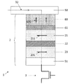
さらに、当該方法は、多層分極層60の界面での混合を最小限にすることを可能にする一方で、強磁性層21、23及びトンネル障壁層22が、予め設定された高い第1アニーリング温度でアニールされ、150%以上の高いトンネル磁気抵抗を可能にする。
2 磁気トンネル接合
21 第1強磁性層
211 第1磁化
22 トンネル障壁層
23 第2強磁性層
231 第2磁化
3 選択トランジスタ
30 前端層
32 スピン分極電流
50 第1導電線、第1電極
51 第2導電線、第2電極
60 分極層
600 磁化極性
61 金属分離層
Claims (8)
- スピン分極電流によって書き込まれる磁気トンネル接合を製造するための方法であって、前記磁気トンネル接合は、一定の向きの第1磁化を有する第1強磁性層と自由に偏向可能な第2磁化を有する第2強磁性層との間のトンネル障壁層、及び磁化極性を有する分極層を備える当該方法において、
この方法は、
前記第1強磁性層、前記トンネル障壁層及び前記第2強磁性層を堆積するステップと、
前記磁気トンネル接合のトンネル磁気抵抗が、約150%以上であるように、当該堆積された第1強磁性層及び第2強磁性層を第1アニーリング温度でアニールするステップと、
前記分極層を堆積するステップと、
前記磁化極性を前記第1磁化及び前記第2磁化に対してほぼ垂直に向けさせるため、当該堆積された分極層を第2アニーリング温度でアニールするステップとから成り、
当該堆積された第1強磁性層及び第2強磁性層の、前記第1アニーリング温度での当該アニーリングは、前記分極層を堆積する前に実施される方法。 - 前記第2アニーリング温度は、前記第1アニーリング温度より低い請求項1に記載の方法。
- 前記第1アニーリング温度は、約340℃〜360℃である請求項1に記載の方法。
- 予め設定された前記第2アニーリング温度は、約150℃〜250℃である請求項1に記載の方法。
- 前記第2強磁性層と前記トンネル障壁層と前記第1強磁性層とを堆積するステップは、この順番で実施される請求項1に記載の方法。
- 前記第1強磁性層と前記トンネル障壁層と前記第2強磁性層とを堆積するステップは、この順番で実施される請求項1に記載の方法。
- 磁気トンネル接合を備えるMRAMセルにおいて、
このMRAMセルは、一定の向きの第1磁化を有する第1強磁性層と自由に偏向可能な第2磁化を有する第2強磁性層との間のトンネル障壁層、並びに前記第1磁化及び前記第2磁化に対してほぼ垂直に向けさせる磁化極性を有する分極層を備え、
前記磁気トンネル接合のトンネル磁気抵抗が、約150%以上であるように、前記第1強磁性層及び第2強磁性層はアニールされるMRAMセル。 - 複数のMRAMセルを備える磁気メモリ装置において、
各MRAMセルは、一定の向きの第1磁化を有する第1強磁性層と自由に偏向可能な第2磁化を有する第2強磁性層との間のトンネル障壁層、並びに前記第1磁化及び前記第2磁化に対してほぼ垂直に向けさせる磁化極性を有する分極層を備え、
前記磁気トンネル接合のトンネル磁気抵抗が、約150%以上であるように、前記第1強磁性層及び第2強磁性層はアニールされる磁気メモリ装置。
Applications Claiming Priority (2)
| Application Number | Priority Date | Filing Date | Title |
|---|---|---|---|
| EP11290013.9 | 2011-01-13 | ||
| EP11290013.9A EP2477227B1 (en) | 2011-01-13 | 2011-01-13 | Magnetic tunnel junction comprising a polarizing layer |
Publications (2)
| Publication Number | Publication Date |
|---|---|
| JP2012146984A true JP2012146984A (ja) | 2012-08-02 |
| JP5903278B2 JP5903278B2 (ja) | 2016-04-13 |
Family
ID=44246134
Family Applications (1)
| Application Number | Title | Priority Date | Filing Date |
|---|---|---|---|
| JP2012003704A Active JP5903278B2 (ja) | 2011-01-13 | 2012-01-12 | 分極層を備える磁気トンネル接合 |
Country Status (6)
| Country | Link |
|---|---|
| US (1) | US8609439B2 (ja) |
| EP (1) | EP2477227B1 (ja) |
| JP (1) | JP5903278B2 (ja) |
| KR (1) | KR20120082359A (ja) |
| RU (1) | RU2573756C2 (ja) |
| TW (1) | TWI535085B (ja) |
Cited By (3)
| Publication number | Priority date | Publication date | Assignee | Title |
|---|---|---|---|---|
| JP2014183279A (ja) * | 2013-03-21 | 2014-09-29 | Tokyo Electron Ltd | 磁気アニール装置 |
| JP2015525426A (ja) * | 2012-05-31 | 2015-09-03 | ノースロップ グラマン システムズ コーポレイションNorthrop Grumman Systems Corporation | ジョセフソン磁気メモリセルシステム |
| US10297481B2 (en) | 2013-03-21 | 2019-05-21 | Tokyo Electron Limited | Magnetic annealing apparatus |
Families Citing this family (80)
| Publication number | Priority date | Publication date | Assignee | Title |
|---|---|---|---|---|
| EP2479759A1 (en) * | 2011-01-19 | 2012-07-25 | Crocus Technology S.A. | Low power magnetic random access memory cell |
| US9236560B1 (en) | 2014-12-08 | 2016-01-12 | Western Digital (Fremont), Llc | Spin transfer torque tunneling magnetoresistive device having a laminated free layer with perpendicular magnetic anisotropy |
| US9502642B2 (en) | 2015-04-10 | 2016-11-22 | Micron Technology, Inc. | Magnetic tunnel junctions, methods used while forming magnetic tunnel junctions, and methods of forming magnetic tunnel junctions |
| US9530959B2 (en) | 2015-04-15 | 2016-12-27 | Micron Technology, Inc. | Magnetic tunnel junctions |
| US9520553B2 (en) | 2015-04-15 | 2016-12-13 | Micron Technology, Inc. | Methods of forming a magnetic electrode of a magnetic tunnel junction and methods of forming a magnetic tunnel junction |
| US9728712B2 (en) | 2015-04-21 | 2017-08-08 | Spin Transfer Technologies, Inc. | Spin transfer torque structure for MRAM devices having a spin current injection capping layer |
| US10468590B2 (en) | 2015-04-21 | 2019-11-05 | Spin Memory, Inc. | High annealing temperature perpendicular magnetic anisotropy structure for magnetic random access memory |
| US9257136B1 (en) | 2015-05-05 | 2016-02-09 | Micron Technology, Inc. | Magnetic tunnel junctions |
| US9960346B2 (en) | 2015-05-07 | 2018-05-01 | Micron Technology, Inc. | Magnetic tunnel junctions |
| US9853206B2 (en) | 2015-06-16 | 2017-12-26 | Spin Transfer Technologies, Inc. | Precessional spin current structure for MRAM |
| US9773974B2 (en) | 2015-07-30 | 2017-09-26 | Spin Transfer Technologies, Inc. | Polishing stop layer(s) for processing arrays of semiconductor elements |
| US10163479B2 (en) | 2015-08-14 | 2018-12-25 | Spin Transfer Technologies, Inc. | Method and apparatus for bipolar memory write-verify |
| US9741926B1 (en) | 2016-01-28 | 2017-08-22 | Spin Transfer Technologies, Inc. | Memory cell having magnetic tunnel junction and thermal stability enhancement layer |
| US9680089B1 (en) | 2016-05-13 | 2017-06-13 | Micron Technology, Inc. | Magnetic tunnel junctions |
| US10460781B2 (en) | 2016-09-27 | 2019-10-29 | Spin Memory, Inc. | Memory device with a dual Y-multiplexer structure for performing two simultaneous operations on the same row of a memory bank |
| US10628316B2 (en) | 2016-09-27 | 2020-04-21 | Spin Memory, Inc. | Memory device with a plurality of memory banks where each memory bank is associated with a corresponding memory instruction pipeline and a dynamic redundancy register |
| US10546625B2 (en) | 2016-09-27 | 2020-01-28 | Spin Memory, Inc. | Method of optimizing write voltage based on error buffer occupancy |
| US10818331B2 (en) | 2016-09-27 | 2020-10-27 | Spin Memory, Inc. | Multi-chip module for MRAM devices with levels of dynamic redundancy registers |
| US10360964B2 (en) | 2016-09-27 | 2019-07-23 | Spin Memory, Inc. | Method of writing contents in memory during a power up sequence using a dynamic redundancy register in a memory device |
| US11119936B2 (en) | 2016-09-27 | 2021-09-14 | Spin Memory, Inc. | Error cache system with coarse and fine segments for power optimization |
| US11119910B2 (en) | 2016-09-27 | 2021-09-14 | Spin Memory, Inc. | Heuristics for selecting subsegments for entry in and entry out operations in an error cache system with coarse and fine grain segments |
| US10437491B2 (en) | 2016-09-27 | 2019-10-08 | Spin Memory, Inc. | Method of processing incomplete memory operations in a memory device during a power up sequence and a power down sequence using a dynamic redundancy register |
| US10991410B2 (en) | 2016-09-27 | 2021-04-27 | Spin Memory, Inc. | Bi-polar write scheme |
| US10366774B2 (en) | 2016-09-27 | 2019-07-30 | Spin Memory, Inc. | Device with dynamic redundancy registers |
| US10437723B2 (en) | 2016-09-27 | 2019-10-08 | Spin Memory, Inc. | Method of flushing the contents of a dynamic redundancy register to a secure storage area during a power down in a memory device |
| US11151042B2 (en) | 2016-09-27 | 2021-10-19 | Integrated Silicon Solution, (Cayman) Inc. | Error cache segmentation for power reduction |
| US10446210B2 (en) | 2016-09-27 | 2019-10-15 | Spin Memory, Inc. | Memory instruction pipeline with a pre-read stage for a write operation for reducing power consumption in a memory device that uses dynamic redundancy registers |
| US10665777B2 (en) | 2017-02-28 | 2020-05-26 | Spin Memory, Inc. | Precessional spin current structure with non-magnetic insertion layer for MRAM |
| US10672976B2 (en) | 2017-02-28 | 2020-06-02 | Spin Memory, Inc. | Precessional spin current structure with high in-plane magnetization for MRAM |
| US10032978B1 (en) | 2017-06-27 | 2018-07-24 | Spin Transfer Technologies, Inc. | MRAM with reduced stray magnetic fields |
| US10656994B2 (en) | 2017-10-24 | 2020-05-19 | Spin Memory, Inc. | Over-voltage write operation of tunnel magnet-resistance (“TMR”) memory device and correcting failure bits therefrom by using on-the-fly bit failure detection and bit redundancy remapping techniques |
| US10489245B2 (en) | 2017-10-24 | 2019-11-26 | Spin Memory, Inc. | Forcing stuck bits, waterfall bits, shunt bits and low TMR bits to short during testing and using on-the-fly bit failure detection and bit redundancy remapping techniques to correct them |
| US10529439B2 (en) | 2017-10-24 | 2020-01-07 | Spin Memory, Inc. | On-the-fly bit failure detection and bit redundancy remapping techniques to correct for fixed bit defects |
| US10481976B2 (en) | 2017-10-24 | 2019-11-19 | Spin Memory, Inc. | Forcing bits as bad to widen the window between the distributions of acceptable high and low resistive bits thereby lowering the margin and increasing the speed of the sense amplifiers |
| US10679685B2 (en) | 2017-12-27 | 2020-06-09 | Spin Memory, Inc. | Shared bit line array architecture for magnetoresistive memory |
| US10395712B2 (en) | 2017-12-28 | 2019-08-27 | Spin Memory, Inc. | Memory array with horizontal source line and sacrificial bitline per virtual source |
| US10360962B1 (en) | 2017-12-28 | 2019-07-23 | Spin Memory, Inc. | Memory array with individually trimmable sense amplifiers |
| US10395711B2 (en) | 2017-12-28 | 2019-08-27 | Spin Memory, Inc. | Perpendicular source and bit lines for an MRAM array |
| US10424726B2 (en) | 2017-12-28 | 2019-09-24 | Spin Memory, Inc. | Process for improving photoresist pillar adhesion during MRAM fabrication |
| US10811594B2 (en) | 2017-12-28 | 2020-10-20 | Spin Memory, Inc. | Process for hard mask development for MRAM pillar formation using photolithography |
| US10891997B2 (en) | 2017-12-28 | 2021-01-12 | Spin Memory, Inc. | Memory array with horizontal source line and a virtual source line |
| US10516094B2 (en) | 2017-12-28 | 2019-12-24 | Spin Memory, Inc. | Process for creating dense pillars using multiple exposures for MRAM fabrication |
| US10840439B2 (en) | 2017-12-29 | 2020-11-17 | Spin Memory, Inc. | Magnetic tunnel junction (MTJ) fabrication methods and systems |
| US10236047B1 (en) | 2017-12-29 | 2019-03-19 | Spin Memory, Inc. | Shared oscillator (STNO) for MRAM array write-assist in orthogonal STT-MRAM |
| US10784439B2 (en) | 2017-12-29 | 2020-09-22 | Spin Memory, Inc. | Precessional spin current magnetic tunnel junction devices and methods of manufacture |
| US10886330B2 (en) | 2017-12-29 | 2021-01-05 | Spin Memory, Inc. | Memory device having overlapping magnetic tunnel junctions in compliance with a reference pitch |
| US10236048B1 (en) | 2017-12-29 | 2019-03-19 | Spin Memory, Inc. | AC current write-assist in orthogonal STT-MRAM |
| US10270027B1 (en) | 2017-12-29 | 2019-04-23 | Spin Memory, Inc. | Self-generating AC current assist in orthogonal STT-MRAM |
| US10840436B2 (en) | 2017-12-29 | 2020-11-17 | Spin Memory, Inc. | Perpendicular magnetic anisotropy interface tunnel junction devices and methods of manufacture |
| US10199083B1 (en) | 2017-12-29 | 2019-02-05 | Spin Transfer Technologies, Inc. | Three-terminal MRAM with ac write-assist for low read disturb |
| US10367139B2 (en) | 2017-12-29 | 2019-07-30 | Spin Memory, Inc. | Methods of manufacturing magnetic tunnel junction devices |
| US10360961B1 (en) | 2017-12-29 | 2019-07-23 | Spin Memory, Inc. | AC current pre-charge write-assist in orthogonal STT-MRAM |
| US10546624B2 (en) | 2017-12-29 | 2020-01-28 | Spin Memory, Inc. | Multi-port random access memory |
| US10424723B2 (en) | 2017-12-29 | 2019-09-24 | Spin Memory, Inc. | Magnetic tunnel junction devices including an optimization layer |
| US10319900B1 (en) | 2017-12-30 | 2019-06-11 | Spin Memory, Inc. | Perpendicular magnetic tunnel junction device with precessional spin current layer having a modulated moment density |
| US10141499B1 (en) | 2017-12-30 | 2018-11-27 | Spin Transfer Technologies, Inc. | Perpendicular magnetic tunnel junction device with offset precessional spin current layer |
| US10255962B1 (en) | 2017-12-30 | 2019-04-09 | Spin Memory, Inc. | Microwave write-assist in orthogonal STT-MRAM |
| US10339993B1 (en) | 2017-12-30 | 2019-07-02 | Spin Memory, Inc. | Perpendicular magnetic tunnel junction device with skyrmionic assist layers for free layer switching |
| US10229724B1 (en) | 2017-12-30 | 2019-03-12 | Spin Memory, Inc. | Microwave write-assist in series-interconnected orthogonal STT-MRAM devices |
| US10236439B1 (en) | 2017-12-30 | 2019-03-19 | Spin Memory, Inc. | Switching and stability control for perpendicular magnetic tunnel junction device |
| US10468588B2 (en) | 2018-01-05 | 2019-11-05 | Spin Memory, Inc. | Perpendicular magnetic tunnel junction device with skyrmionic enhancement layers for the precessional spin current magnetic layer |
| US10438996B2 (en) | 2018-01-08 | 2019-10-08 | Spin Memory, Inc. | Methods of fabricating magnetic tunnel junctions integrated with selectors |
| US10438995B2 (en) | 2018-01-08 | 2019-10-08 | Spin Memory, Inc. | Devices including magnetic tunnel junctions integrated with selectors |
| US10446744B2 (en) | 2018-03-08 | 2019-10-15 | Spin Memory, Inc. | Magnetic tunnel junction wafer adaptor used in magnetic annealing furnace and method of using the same |
| US10388861B1 (en) | 2018-03-08 | 2019-08-20 | Spin Memory, Inc. | Magnetic tunnel junction wafer adaptor used in magnetic annealing furnace and method of using the same |
| US10734573B2 (en) | 2018-03-23 | 2020-08-04 | Spin Memory, Inc. | Three-dimensional arrays with magnetic tunnel junction devices including an annular discontinued free magnetic layer and a planar reference magnetic layer |
| US11107974B2 (en) | 2018-03-23 | 2021-08-31 | Spin Memory, Inc. | Magnetic tunnel junction devices including a free magnetic trench layer and a planar reference magnetic layer |
| US11107978B2 (en) | 2018-03-23 | 2021-08-31 | Spin Memory, Inc. | Methods of manufacturing three-dimensional arrays with MTJ devices including a free magnetic trench layer and a planar reference magnetic layer |
| US10784437B2 (en) | 2018-03-23 | 2020-09-22 | Spin Memory, Inc. | Three-dimensional arrays with MTJ devices including a free magnetic trench layer and a planar reference magnetic layer |
| US10411185B1 (en) | 2018-05-30 | 2019-09-10 | Spin Memory, Inc. | Process for creating a high density magnetic tunnel junction array test platform |
| US10692569B2 (en) | 2018-07-06 | 2020-06-23 | Spin Memory, Inc. | Read-out techniques for multi-bit cells |
| US10593396B2 (en) | 2018-07-06 | 2020-03-17 | Spin Memory, Inc. | Multi-bit cell read-out techniques for MRAM cells with mixed pinned magnetization orientations |
| US10559338B2 (en) | 2018-07-06 | 2020-02-11 | Spin Memory, Inc. | Multi-bit cell read-out techniques |
| US10600478B2 (en) | 2018-07-06 | 2020-03-24 | Spin Memory, Inc. | Multi-bit cell read-out techniques for MRAM cells with mixed pinned magnetization orientations |
| US10650875B2 (en) | 2018-08-21 | 2020-05-12 | Spin Memory, Inc. | System for a wide temperature range nonvolatile memory |
| US10699761B2 (en) | 2018-09-18 | 2020-06-30 | Spin Memory, Inc. | Word line decoder memory architecture |
| US10971680B2 (en) | 2018-10-01 | 2021-04-06 | Spin Memory, Inc. | Multi terminal device stack formation methods |
| US11621293B2 (en) | 2018-10-01 | 2023-04-04 | Integrated Silicon Solution, (Cayman) Inc. | Multi terminal device stack systems and methods |
| US10580827B1 (en) | 2018-11-16 | 2020-03-03 | Spin Memory, Inc. | Adjustable stabilizer/polarizer method for MRAM with enhanced stability and efficient switching |
| US11107979B2 (en) | 2018-12-28 | 2021-08-31 | Spin Memory, Inc. | Patterned silicide structures and methods of manufacture |
Citations (8)
| Publication number | Priority date | Publication date | Assignee | Title |
|---|---|---|---|---|
| JP2003092444A (ja) * | 2001-07-13 | 2003-03-28 | Alps Electric Co Ltd | 磁気検出素子の製造方法 |
| JP2006128579A (ja) * | 2004-11-01 | 2006-05-18 | Sony Corp | 記憶素子及びメモリ |
| JP2006179524A (ja) * | 2004-12-20 | 2006-07-06 | Toshiba Corp | 磁気記録素子、磁気記録装置、および情報の記録方法 |
| US20070297220A1 (en) * | 2006-06-22 | 2007-12-27 | Masatoshi Yoshikawa | Magnetoresistive element and magnetic memory |
| JP2008028362A (ja) * | 2006-06-22 | 2008-02-07 | Toshiba Corp | 磁気抵抗素子及び磁気メモリ |
| US20080151614A1 (en) * | 2006-12-22 | 2008-06-26 | Magic Technologies, Inc. | Spin transfer MRAM device with magnetic biasing |
| WO2009122992A1 (ja) * | 2008-04-03 | 2009-10-08 | 日本電気株式会社 | 磁気抵抗記憶装置 |
| WO2010100728A1 (ja) * | 2009-03-04 | 2010-09-10 | 株式会社日立製作所 | 磁気メモリ |
Family Cites Families (7)
| Publication number | Priority date | Publication date | Assignee | Title |
|---|---|---|---|---|
| US5583725A (en) | 1994-06-15 | 1996-12-10 | International Business Machines Corporation | Spin valve magnetoresistive sensor with self-pinned laminated layer and magnetic recording system using the sensor |
| US5695864A (en) | 1995-09-28 | 1997-12-09 | International Business Machines Corporation | Electronic device using magnetic components |
| US5640343A (en) | 1996-03-18 | 1997-06-17 | International Business Machines Corporation | Magnetic memory array using magnetic tunnel junction devices in the memory cells |
| FR2817999B1 (fr) | 2000-12-07 | 2003-01-10 | Commissariat Energie Atomique | Dispositif magnetique a polarisation de spin et a empilement(s) tri-couche(s) et memoire utilisant ce dispositif |
| US7270896B2 (en) * | 2004-07-02 | 2007-09-18 | International Business Machines Corporation | High performance magnetic tunnel barriers with amorphous materials |
| US7241631B2 (en) * | 2004-12-29 | 2007-07-10 | Grandis, Inc. | MTJ elements with high spin polarization layers configured for spin-transfer switching and spintronics devices using the magnetic elements |
| RU2394304C2 (ru) * | 2007-12-26 | 2010-07-10 | Федеральное государственное бюджетное образовательное учреждение высшего профессионального образования "Национальный исследовательский ядерный университет МИФИ" (НИЯУ МИФИ) | Способ формирования структуры магнитного туннельного перехода на основе наноразмерных структур металл-изолятор-металл и структура магнитного туннельного перехода на основе наноразмерных структур металл-изолятор-металл (варианты) |
-
2011
- 2011-01-13 EP EP11290013.9A patent/EP2477227B1/en active Active
-
2012
- 2012-01-11 KR KR1020120003436A patent/KR20120082359A/ko not_active Withdrawn
- 2012-01-11 TW TW101101022A patent/TWI535085B/zh not_active IP Right Cessation
- 2012-01-12 US US13/348,996 patent/US8609439B2/en active Active
- 2012-01-12 JP JP2012003704A patent/JP5903278B2/ja active Active
- 2012-01-12 RU RU2012101118/08A patent/RU2573756C2/ru active
Patent Citations (11)
| Publication number | Priority date | Publication date | Assignee | Title |
|---|---|---|---|---|
| JP2003092444A (ja) * | 2001-07-13 | 2003-03-28 | Alps Electric Co Ltd | 磁気検出素子の製造方法 |
| US20030163913A1 (en) * | 2001-07-13 | 2003-09-04 | Naoya Hasegawa | Method for manufacturing magnetic sensing element having improved magnetic field sensitivity |
| JP2006128579A (ja) * | 2004-11-01 | 2006-05-18 | Sony Corp | 記憶素子及びメモリ |
| JP2006179524A (ja) * | 2004-12-20 | 2006-07-06 | Toshiba Corp | 磁気記録素子、磁気記録装置、および情報の記録方法 |
| US20070297220A1 (en) * | 2006-06-22 | 2007-12-27 | Masatoshi Yoshikawa | Magnetoresistive element and magnetic memory |
| JP2008028362A (ja) * | 2006-06-22 | 2008-02-07 | Toshiba Corp | 磁気抵抗素子及び磁気メモリ |
| US20080151614A1 (en) * | 2006-12-22 | 2008-06-26 | Magic Technologies, Inc. | Spin transfer MRAM device with magnetic biasing |
| WO2009122992A1 (ja) * | 2008-04-03 | 2009-10-08 | 日本電気株式会社 | 磁気抵抗記憶装置 |
| WO2010100728A1 (ja) * | 2009-03-04 | 2010-09-10 | 株式会社日立製作所 | 磁気メモリ |
| EP2405504A1 (en) * | 2009-03-04 | 2012-01-11 | Hitachi, Ltd. | Magnetic memory |
| US20120012955A1 (en) * | 2009-03-04 | 2012-01-19 | Hitachi, Ltd. | Magnetic memory |
Cited By (3)
| Publication number | Priority date | Publication date | Assignee | Title |
|---|---|---|---|---|
| JP2015525426A (ja) * | 2012-05-31 | 2015-09-03 | ノースロップ グラマン システムズ コーポレイションNorthrop Grumman Systems Corporation | ジョセフソン磁気メモリセルシステム |
| JP2014183279A (ja) * | 2013-03-21 | 2014-09-29 | Tokyo Electron Ltd | 磁気アニール装置 |
| US10297481B2 (en) | 2013-03-21 | 2019-05-21 | Tokyo Electron Limited | Magnetic annealing apparatus |
Also Published As
| Publication number | Publication date |
|---|---|
| RU2573756C2 (ru) | 2016-01-27 |
| TW201234691A (en) | 2012-08-16 |
| JP5903278B2 (ja) | 2016-04-13 |
| TWI535085B (zh) | 2016-05-21 |
| RU2012101118A (ru) | 2013-07-20 |
| US8609439B2 (en) | 2013-12-17 |
| EP2477227B1 (en) | 2019-03-27 |
| US20120181642A1 (en) | 2012-07-19 |
| EP2477227A1 (en) | 2012-07-18 |
| KR20120082359A (ko) | 2012-07-23 |
Similar Documents
| Publication | Publication Date | Title |
|---|---|---|
| JP5903278B2 (ja) | 分極層を備える磁気トンネル接合 | |
| EP2249350B1 (en) | Magnetic memory with a thermally assisted spin transfer torque writing procedure using a low writing current | |
| KR102353406B1 (ko) | 스핀 궤도 토크를 이용하여 강화된 감쇠 프로그램 및 경사진 자화 용이축을 갖는 자기 접합부를 포함하는 자기 소자 | |
| US10953319B2 (en) | Spin transfer MRAM element having a voltage bias control | |
| JP6088167B2 (ja) | 半金属強磁性体を用いた磁気接合を提供するための方法及びシステム | |
| KR102145269B1 (ko) | 스핀 전달 토크 자기 램의 응용 분야들에서 사용할 수 있는 이중 수직 자기 이방성 자기 접합 | |
| US20150129996A1 (en) | Method and system for providing a top pinned layer perpendicular magnetic anisotropy magnetic junction usable in spin transfer torque magnetic random access memory applications | |
| US9508924B2 (en) | Method and system for providing rare earth magnetic junctions usable in spin transfer torque magnetic random access memory applications | |
| JP2012104825A (ja) | スイッチングが改良されたハイブリッド磁気トンネル接合要素を提供するための方法およびシステム | |
| KR20150054664A (ko) | 스핀 전달 토크 자기 램의 응용 분야에서 사용될 수 있는 수직 자기 접합의 벌크 수직 자기 이방성 자유 층을 제공하는 방법 및 시스템 | |
| EP2528060B1 (en) | Multibit cell with synthetic storage layer | |
| TW201939494A (zh) | 磁性裝置、使用其的磁性記憶體及用於提供其的方法 | |
| JP2012151476A (ja) | 低電力磁気ランダムアクセスメモリセル | |
| KR102486310B1 (ko) | 열적으로 보조되는 스핀 토크 전가 스위칭을 이용한 자기 접합을 제공하는 방법 및 시스템 | |
| TW201724597A (zh) | 磁性接面、磁性記憶體以及將該磁性接面程式化的方法 | |
| US9917249B2 (en) | Method and system for providing a magnetic junction usable in spin transfer torque applications and including a magnetic barrier layer | |
| EP2249349A1 (en) | Magnetic memory with a thermally assisted writing procedure and reduced writng field | |
| CN103137853A (zh) | 存储元件和存储设备 | |
| US10276225B2 (en) | Method and system for providing a magnetic junction usable in spin transfer or spin-orbit torque applications and including a magnetic barrier layer | |
| US9472750B2 (en) | Method and system for providing a bottom pinned layer in a perpendicular magnetic junction usable in spin transfer torque magnetic random access memory applications | |
| KR102480077B1 (ko) | 마그네틱 장치에서 이용가능하고 기판 상에 위치하는 마그네틱 접합 및 그의 제조 방법 | |
| US10438638B2 (en) | Method and system for providing a magnetic layer in a magnetic junction usable in spin transfer or spin orbit torque applications using a sacrificial oxide layer | |
| US10079337B2 (en) | Double magnetic tunnel junction with dynamic reference layer |
Legal Events
| Date | Code | Title | Description |
|---|---|---|---|
| A621 | Written request for application examination |
Free format text: JAPANESE INTERMEDIATE CODE: A621 Effective date: 20140725 |
|
| A131 | Notification of reasons for refusal |
Free format text: JAPANESE INTERMEDIATE CODE: A131 Effective date: 20150430 |
|
| A977 | Report on retrieval |
Free format text: JAPANESE INTERMEDIATE CODE: A971007 Effective date: 20150430 |
|
| A521 | Request for written amendment filed |
Free format text: JAPANESE INTERMEDIATE CODE: A523 Effective date: 20150723 |
|
| A131 | Notification of reasons for refusal |
Free format text: JAPANESE INTERMEDIATE CODE: A131 Effective date: 20151118 |
|
| A521 | Request for written amendment filed |
Free format text: JAPANESE INTERMEDIATE CODE: A523 Effective date: 20160205 |
|
| TRDD | Decision of grant or rejection written | ||
| A01 | Written decision to grant a patent or to grant a registration (utility model) |
Free format text: JAPANESE INTERMEDIATE CODE: A01 Effective date: 20160224 |
|
| A61 | First payment of annual fees (during grant procedure) |
Free format text: JAPANESE INTERMEDIATE CODE: A61 Effective date: 20160314 |
|
| R150 | Certificate of patent or registration of utility model |
Ref document number: 5903278 Country of ref document: JP Free format text: JAPANESE INTERMEDIATE CODE: R150 |
|
| R250 | Receipt of annual fees |
Free format text: JAPANESE INTERMEDIATE CODE: R250 |
|
| R250 | Receipt of annual fees |
Free format text: JAPANESE INTERMEDIATE CODE: R250 |
|
| R250 | Receipt of annual fees |
Free format text: JAPANESE INTERMEDIATE CODE: R250 |
|
| R250 | Receipt of annual fees |
Free format text: JAPANESE INTERMEDIATE CODE: R250 |
|
| R250 | Receipt of annual fees |
Free format text: JAPANESE INTERMEDIATE CODE: R250 |
|
| S531 | Written request for registration of change of domicile |
Free format text: JAPANESE INTERMEDIATE CODE: R313531 |
|
| R350 | Written notification of registration of transfer |
Free format text: JAPANESE INTERMEDIATE CODE: R350 |
|
| R250 | Receipt of annual fees |
Free format text: JAPANESE INTERMEDIATE CODE: R250 |
|
| S111 | Request for change of ownership or part of ownership |
Free format text: JAPANESE INTERMEDIATE CODE: R313113 |
|
| R350 | Written notification of registration of transfer |
Free format text: JAPANESE INTERMEDIATE CODE: R350 |
|
| R250 | Receipt of annual fees |
Free format text: JAPANESE INTERMEDIATE CODE: R250 |