JP2012147632A - Power transmission device and power transmission method - Google Patents
Power transmission device and power transmission method Download PDFInfo
- Publication number
- JP2012147632A JP2012147632A JP2011005944A JP2011005944A JP2012147632A JP 2012147632 A JP2012147632 A JP 2012147632A JP 2011005944 A JP2011005944 A JP 2011005944A JP 2011005944 A JP2011005944 A JP 2011005944A JP 2012147632 A JP2012147632 A JP 2012147632A
- Authority
- JP
- Japan
- Prior art keywords
- power
- power transmission
- power receiving
- unit
- capacitor
- Prior art date
- Legal status (The legal status is an assumption and is not a legal conclusion. Google has not performed a legal analysis and makes no representation as to the accuracy of the status listed.)
- Pending
Links
Images





Landscapes
- Charge And Discharge Circuits For Batteries Or The Like (AREA)
Abstract
【課題】効率的に適切な電力を受電装置に給電する。
【解決手段】送電部11は受電装置20,21に対して非接触で送電し、電源部12は送電部11が送電する電力を生成し、検出部13は受電装置20,21の台数を検出し、整合部14は、受電装置20,21の台数に対応したコンデンサ素子C1〜C3とインダクタ素子L1〜L3の組を複数有し、検出された受電装置20,21の台数に応じて、選択するコンデンサ素子C1〜C3とインダクタ素子L1〜L3の組を変更することで送電部11と電源部12との間のインピーダンス整合を行う。
【選択図】図1Efficient power is efficiently supplied to a power receiving apparatus.
A power transmission unit 11 transmits power to a power receiving device 20, 21 in a non-contact manner, a power source unit 12 generates electric power transmitted by the power transmission unit 11, and a detection unit 13 detects the number of the power receiving devices 20, 21. The matching unit 14 has a plurality of sets of capacitor elements C1 to C3 and inductor elements L1 to L3 corresponding to the number of power receiving devices 20 and 21, and is selected according to the number of detected power receiving devices 20 and 21. Impedance matching between the power transmission unit 11 and the power supply unit 12 is performed by changing the combination of the capacitor elements C1 to C3 and the inductor elements L1 to L3.
[Selection] Figure 1
Description
本発明は、電力伝送装置及び電力伝送方法に関する。 The present invention relates to a power transmission device and a power transmission method.
非接触で電力を伝送する技術として、電磁誘導方式と電波収穫方式が知られているが、これらに代わる新たな方式として、近年、近傍磁界中の共鳴現象を利用した方式(以下磁界共鳴方式と呼ぶ)が提唱された。 The electromagnetic induction method and the radio wave harvesting method are known as non-contact power transmission technologies. However, as a new method to replace these methods, a method using a resonance phenomenon in a near magnetic field (hereinafter referred to as a magnetic field resonance method) has recently been used. Called).
磁界共鳴方式は、送受電側双方に、高いQ値を持つ略同一共振周波数のコイルを配置し、磁界を媒介とする共鳴状態にすることで、高効率の電力伝送を可能とするものである。この方式によれば、従来から知られている電磁誘導方式よりも、長距離の電力伝送が可能であり、且つ受電装置の位置ずれにも強く、携帯電話などのモバイル機器をはじめ、家電製品、電気自動車など様々な電子機器への適用が期待されている。 In the magnetic field resonance system, coils with substantially the same resonance frequency having a high Q value are arranged on both the power transmission and reception sides, and a resonance state using a magnetic field as a medium enables high-efficiency power transmission. . According to this method, it is possible to transmit power over a longer distance than the conventionally known electromagnetic induction method, and it is also resistant to displacement of the power receiving device, including mobile devices such as mobile phones, home appliances, Application to various electronic devices such as electric vehicles is expected.
ところで、効率よく受電装置に電力伝送を行うため、送電側の装置の送電アンプとその接続先のインピーダンスを整合することが求められる。すなわち、送電アンプと、その接続先のインピーダンス不整合によって電力反射が生じることを抑えることが求められる。 By the way, in order to efficiently transmit power to the power receiving device, it is required to match the power transmission amplifier of the power transmission side device with the impedance of the connection destination. That is, it is required to suppress the occurrence of power reflection due to impedance mismatch between the power transmission amplifier and its connection destination.
従来、磁界共鳴方式を利用した電力伝送システムにおいて、送電装置の送電アンプと送電コイルの間にインダクタ素子と可変コンデンサを有した整合回路を挿入し、送電装置と受電装置間の距離や負荷の変化に応じてインピーダンス整合を行う手法が知られている。 Conventionally, in a power transmission system using a magnetic field resonance method, a matching circuit having an inductor element and a variable capacitor is inserted between a power transmission amplifier and a power transmission coil of a power transmission device, and a change in distance and load between the power transmission device and the power reception device. There is known a technique for performing impedance matching according to the above.
しかし、従来の技術では、受電装置の台数が変化する場合、送電部の負荷が大きく変化するためインピーダンス調整に時間がかかり、効率的に適切な電力を受電装置に給電することが困難であるという問題があった。 However, in the conventional technology, when the number of power receiving devices changes, the load of the power transmission unit changes greatly, so that impedance adjustment takes time, and it is difficult to efficiently supply appropriate power to the power receiving device. There was a problem.
発明の一観点によれば、受電装置に対して非接触で送電する送電部と、前記送電部が送電する電力を生成する電源部と、前記受電装置の台数を検出する検出部と、前記受電装置の台数に対応したコンデンサ素子とインダクタ素子の組を複数有し、検出された前記受電装置の台数に応じて、選択する前記コンデンサ素子と前記インダクタ素子の組を変更することで前記送電部と前記電源部との間のインピーダンス整合を行う整合部と、を備えた電力伝送装置が提供される。 According to an aspect of the invention, a power transmission unit that transmits power to a power reception device in a contactless manner, a power source unit that generates power transmitted by the power transmission unit, a detection unit that detects the number of the power reception devices, and the power reception unit A plurality of sets of capacitor elements and inductor elements corresponding to the number of devices, and changing the set of capacitor elements and inductor elements to be selected according to the number of detected power receiving devices; There is provided a power transmission device including a matching unit that performs impedance matching with the power source unit.
開示の電力伝送装置及び電力伝送方法によれば、効率的に適切な電力を受電装置に給電することができる。 According to the disclosed power transmission device and power transmission method, it is possible to efficiently supply appropriate power to the power receiving device.
以下、本発明の実施の形態を、図面を参照しつつ説明する。
(第1の実施の形態)
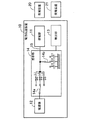
図1は、第1の実施の形態の電力伝送装置の一例を示す図である。
Hereinafter, embodiments of the present invention will be described with reference to the drawings.
(First embodiment)
FIG. 1 is a diagram illustrating an example of a power transmission device according to the first embodiment.
電力伝送装置10は、送電部11、電源部12、検出部13、整合部14を有している。図1の例では、2台の受電装置20,21が示されている。受電装置20,21は、たとえば、携帯電話やラップトップコンピュータなどのモバイル機器、またはその他の電子機器である。
The
送電部11は、受電装置20,21に対して非接触で送電する。電源部12は、受電装置20,21に送電する電力を生成する。検出部13は、たとえば、センサや通信モジュールなどによって受電装置20,21の台数を検出する。
The
整合部14は、送電部11と電源部12との間の伝送線路15に設けられている。
磁界共鳴方式のような非接触で送電する方式では、電波による放送受信などと異なり、近傍界領域でエネルギーの伝送が行われるため、受電装置の台数によって送電部11の入力インピーダンス(負荷)が変化する。送電部11の入力インピーダンスと電源部12の出力インピーダンスが異なると電力反射が起こり、反射損失(リターンロス)が発生して電力伝送効率が低下する。
The
In the non-contact power transmission method such as the magnetic field resonance method, energy transmission is performed in the near-field region unlike broadcast reception using radio waves, and therefore the input impedance (load) of the
そのため、整合部14は、送電部11と電源部12との間のインピーダンス整合を行う。たとえば、整合部14は、送電部11の入力インピーダンスと自身のインピーダンスの合成インピーダンスが、電源部12の出力インピーダンスと等しくなるように調整を行う。送電部11の入力インピーダンスが受電装置の台数によって異なるため、整合部14は、コンデンサ素子C1,C2,C3とインダクタ素子L1,L2,L3の組を台数に対応して複数備えている。
Therefore, the matching
図1に示す例の場合、たとえば、コンデンサ素子C1とインダクタ素子L1の組が、受電装置が1台の場合に用いられる組とする。また、コンデンサ素子C2とインダクタ素子L2の組が、受電装置が2台の場合に用いられる組、コンデンサ素子C3とインダクタ素子L3の組が、受電装置が3台の場合に用いられる組などとする。また、たとえば、コンデンサ素子C3とインダクタ素子L1の組が、受電装置が4台の場合に用いられる組などと対応づけてもよい。 In the case of the example shown in FIG. 1, for example, a set of the capacitor element C1 and the inductor element L1 is set to be used when there is one power receiving device. Further, a set of the capacitor element C2 and the inductor element L2 is a set used when there are two power receiving devices, a set of the capacitor element C3 and the inductor element L3 is a set used when there are three power receiving devices, and the like. . Further, for example, a set of the capacitor element C3 and the inductor element L1 may be associated with a set used when there are four power receiving apparatuses.
受電装置の台数に対応したコンデンサ素子C1〜C3とインダクタ素子L1〜L3の組は、受電装置がその台数の場合に、送電部11と電源部12との間でインピーダンス整合されるようにキャパシタンス及びインダクタンスが設定されている。
A set of capacitor elements C1 to C3 and inductor elements L1 to L3 corresponding to the number of power receiving devices has a capacitance and a capacitance so that impedance matching is performed between the
たとえば、コンデンサ素子C2とインダクタ素子L2の組が、受電装置が2台の場合に用いられる組とする。この場合、コンデンサ素子C2とインダクタ素子L2は、受電装置が2台の場合の送電部11の入力インピーダンスと電源部12の出力インピーダンスが整合するように、キャパシタンス及びインダクタンスが予め設定されているものとする。
For example, a set of the capacitor element C2 and the inductor element L2 is a set used when there are two power receiving apparatuses. In this case, the capacitance and inductance of the capacitor element C2 and the inductor element L2 are set in advance so that the input impedance of the
なお、本明細書中で、インピーダンスが整合するとは、入力インピーダンスと出力インピーダンスの整合が完全にとれている、という意味に限定されない。たとえば、電源部12の出力端の反射係数が0.2以下、すなわち、反射による損失が4%以下であることが望ましい。
In the present specification, matching impedance is not limited to the meaning that input impedance and output impedance are perfectly matched. For example, it is desirable that the reflection coefficient at the output end of the
各コンデンサ素子C1〜C3の一方の端子は、送電部11と電源部12の間の伝送線路15にスイッチ14bを介して接続されており、他方の端子は接地されている。
インダクタ素子L1〜L3は、伝送線路15に接続されており、一方の端子は送電部11に接続され、他方の端子はスイッチ14aを介して電源部12に接続されている。
One terminal of each of the capacitor elements C1 to C3 is connected to the
The inductor elements L1 to L3 are connected to the
整合部14は、検出された受電装置の台数に応じて、スイッチ14a,14bにて、選択するコンデンサ素子とインダクタ素子の組を切り替える。たとえば、図1に示す例の場合、2台の受電装置20,21があるので、整合部14は、2台のときに用いるコンデンサ素子C2とインダクタ素子L2の組を選択する。
The matching
図2は、受電装置が2台から3台に変化した場合の整合部の一例の様子を示す図である。
給電対象の受電装置が、図2に示すように3台(受電装置20,21,22)となった場合、検出部13はこの台数の変化を検出する。そして、検出部13は、整合部14に対して3台に対応したコンデンサ素子とインダクタ素子の組(たとえば、コンデンサ素子C3とインダクタ素子L3)を選択するように指示する。
FIG. 2 is a diagram illustrating an example of a matching unit when the number of power receiving apparatuses is changed from two to three.
When the number of power receiving devices to be fed is three (
指示を受けた整合部14は、スイッチ14a,14bで、使用するコンデンサ素子とインダクタ素子の組を、たとえば、図1の状態から、受電装置が3台の場合に用いるコンデンサ素子C3とインダクタ素子L3の組に切り替える。
Upon receiving the instruction, the
これにより、検出された受電装置の台数に対して適切なインピーダンスを迅速に選択できるようになるので、インピーダンス整合が容易になり、効率的に適切な電力を受電装置に給電することができるようになる。 As a result, it becomes possible to quickly select an appropriate impedance for the number of detected power receiving devices, so that impedance matching is facilitated, and appropriate power can be efficiently supplied to the power receiving devices. Become.
また、空気を誘電体とする高耐圧の可変コンデンサではなく、複数のコンデンサ素子C1〜C3とインダクタ素子L1〜L3の組の切り替えにより受電装置の台数に応じたインピーダンス整合を行うので、電力伝送装置10の小型化が期待できる。可変コンデンサのみでインピーダンス整合を行うようにすると、受電装置の台数の変化などによる入力インピーダンスの大きな変化に対応できるように調整範囲が広がり、容積が大きくなるからである。 In addition, since the impedance matching is performed according to the number of power receiving devices by switching a set of a plurality of capacitor elements C1 to C3 and inductor elements L1 to L3, instead of a high withstand voltage variable capacitor using air as a dielectric, a power transmission device A reduction in size of 10 can be expected. This is because if the impedance matching is performed only with the variable capacitor, the adjustment range is expanded and the volume is increased so as to cope with a large change in input impedance due to a change in the number of power receiving devices.
以下第2の実施の形態として、電力伝送装置をより詳細に説明する。
(第2の実施の形態)
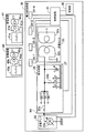
図3は、第2の実施の形態の電力伝送装置の一例を示す図である。
Hereinafter, the power transmission apparatus will be described in more detail as a second embodiment.
(Second Embodiment)
FIG. 3 is a diagram illustrating an example of the power transmission apparatus according to the second embodiment.
電力伝送装置30は、磁界共鳴方式で電力伝送を行うものであり、制御回路31、送電コイル32、送電アンプ33、検出センサ34−1,34−2,34−3,34−4、整合回路35、記憶部36を有している。
The
図3の例では、2台の受電装置40,41が示されている。受電装置40,41は、たとえば、携帯電話やラップトップコンピュータなどのモバイル機器、またはその他の電子機器である。
In the example of FIG. 3, two
制御回路31は、電力伝送装置30の各部を制御する。たとえば、制御回路31は、検出センサ34−1〜34−4からの信号をもとに、給電対象の受電装置の台数を検出する機能(図1に示した検出部13の機能)を有している。また、制御回路31は、送電アンプ33の出力端のノードN1において、送電アンプ33と整合回路35間の電力反射状態(反射係数)を計測する。
The
送電コイル32は、図1に示した送電部11の機能を有し、受電装置40,41に対して送電を行う。送電コイル32は、送電周波数に対応した共振周波数を持つ共振コイル32aと、共振コイル32aに対して非接触で電力を供給する誘導コイル32bを有している。また、共振コイル32aには、コンデンサ素子Crが並列に接続されている。誘導コイル32bの一端は整合回路35に接続されており、他端は接地されている。
The
送電アンプ33は、図1に示した電源部12の機能を有し、交流電源33aにより所定の送電周波数で電力を生成する。また、送電アンプ33は、制御回路31の制御により、検出された受電装置の台数に応じて、生成する電力の大きさを調整する。
The
検出センサ34−1〜34−4は、受電装置40,41を検出する。検出センサ34−1〜34−4は、たとえば、赤外線または、Bluetooth(登録商標)などで通信を行う通信モジュールであり、たとえば、それぞれ1台の受電装置と無線通信を行う。したがって、図3に示す電力伝送装置30の例では、4台の受電装置と同時に通信が可能となっている。たとえば、Bluetoothの場合、障害物がない状態では約10m程度の距離で受電装置の検出が可能である。
The detection sensors 34-1 to 34-4 detect the
なお、検出センサ34−1〜34−4の数は特に限定されるものではない。また、検出センサ34−1〜34−4は、通信モジュールに限定されず、受電装置40,41が電力伝送装置30の充電用治具などに搭載されたことを検出する重量センサでもよい。
The number of detection sensors 34-1 to 34-4 is not particularly limited. The detection sensors 34-1 to 34-4 are not limited to communication modules, and may be weight sensors that detect that the
整合回路35は、送電コイル32と送電アンプ33との間の伝送線路37に設けられており、図1に示した整合部14の機能を有している。
整合回路35は、制御回路31の制御のもと、送電コイル32と送電アンプ33との間のインピーダンス整合を行う。たとえば、整合回路35は、送電コイル32の入力インピーダンスと自身のインピーダンスの合成インピーダンスが、送電アンプ33の出力インピーダンスと等しくなるように調整を行う。送電コイル32の入力インピーダンスが受電装置の台数によって異なるため、整合回路35は、コンデンサ素子C1〜C3とインダクタ素子L1〜L3の組を台数に対応して複数備えている。
The matching
The matching
図3に示した整合回路35の例では、図1に示した例と同様に、コンデンサ素子C1〜C3、インダクタ素子L1〜L3、スイッチ35a,35bを有している。コンデンサ素子C1〜C3は、省スペース化の観点から高誘電率(かつ低損失)のものを使用することが望ましい。
The matching
ここで、たとえば、コンデンサ素子C1とインダクタ素子L1の組が、受電装置が1台の場合に用いられる組とする。また、コンデンサ素子C2とインダクタ素子L2の組が、受電装置が2台の場合に用いられる組、コンデンサ素子C3とインダクタ素子L3の組が、受電装置が3台の場合に用いられる組などとする。また、たとえば、コンデンサ素子C3とインダクタ素子L1の組が、受電装置が4台の場合に用いられる組などと対応づけてもよい。 Here, for example, a set of the capacitor element C1 and the inductor element L1 is a set used when there is one power receiving device. Further, a set of the capacitor element C2 and the inductor element L2 is a set used when there are two power receiving devices, a set of the capacitor element C3 and the inductor element L3 is a set used when there are three power receiving devices, and the like. . Further, for example, a set of the capacitor element C3 and the inductor element L1 may be associated with a set used when there are four power receiving apparatuses.
各コンデンサ素子C1〜C3の一方の端子は、誘導コイル32bと送電アンプ33の間の伝送線路37にスイッチ35bを介して接続されており、他方の端子は接地されている。
One terminal of each of the capacitor elements C1 to C3 is connected to a
インダクタ素子L1〜L3は、伝送線路37に接続されており、一方の端子は送電コイル32における誘導コイル32bに接続され、他方の端子はスイッチ35aを介して送電アンプ33に接続されている。
The inductor elements L1 to L3 are connected to the
スイッチ35a,35bの切り替えは、制御回路31からの制御信号により行われ、検出された受電装置の台数に応じて、選択されるコンデンサ素子とインダクタ素子の組が切り替えられる。たとえば、図3に示す例の場合、2台の受電装置40,41があるので、整合回路35において、2台のときに用いるコンデンサ素子C2とインダクタ素子L2の組が選択される。
The
さらに、本実施の形態において整合回路35は、可変コンデンサCvを有している。可変コンデンサCvの一端は伝送線路37に接続されており、他端は接地されている。可変コンデンサCvは、コンデンサ素子C1〜C3とインダクタ素子L1〜L3の組の切り替えにより、離散的に変化するインピーダンスを補償し、精度よくインピーダンス整合が行われるよう微調整を行うものであるので、小容量のもので済む。可変コンデンサCvは、制御回路31からの制御信号により、容量値が制御される。
Further, in the present embodiment, the matching
記憶部36は、たとえば、給電可能な受電装置の情報(たとえば、磁界共鳴方式に対応している型、品名など)や、給電を許可するユーザの登録情報などを記憶する。
受電装置40,41は、バッテリ40a,41a、誘導コイル40b,41b、共振コイル40c,41c、検出センサ40d,41dを有している。共振コイル40c,41cにはコンデンサ素子Cr1,Cr2が並列に接続されている。
The
The
受電装置40,41は、共振コイル40c,41cにより、電力伝送装置30から電力を受け、誘導コイル40b,41bに電力を伝えて、誘導コイル40b,41bに接続されたバッテリ40a,41aを充電する。検出センサ40d,41dは、電力伝送装置30の検出センサ34−1〜34−4の何れかと通信を行う。
The
検出センサ40d,41dは、電力伝送装置30の検出センサ34−1〜34−4と同様に、たとえば、赤外線または、Bluetoothなどで通信を行う通信モジュールである。
The
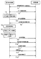
図4は、送電時の電力伝送装置と受電装置における通信シーケンスの一例を示す図である。
以下では一例として、図3に示したような受電装置40,41が存在する場合の送電時の電力伝送装置30の動作を説明する。
FIG. 4 is a diagram illustrating an example of a communication sequence in the power transmission device and the power receiving device during power transmission.
Hereinafter, as an example, the operation of the
電力伝送装置30は、検出センサ34−1〜34−4により、受電装置40,41の検知を行い、受電装置40,41の台数(図3の場合は2台)を検出する(処理T1)。たとえば、検出センサ34−1〜34−4が通信モジュールである場合、受電装置40,41の検出センサ40d,41dとの間で通信が確立した場合に、受電装置40,41が検知される。その後、電力伝送装置30と検知された受電装置40,41との間でデータ通信処理が行われる(処理T2)。データ通信処理では、受電装置40,41の認証やワイヤレスで充電するためのデータについてのやり取りなどが行われる。データの例としては、受電装置40,41の型式や、受電装置40,41を所持するユーザの契約情報、バッテリ40a,41aが対応している電圧やワット数などのバッテリ情報、送電アンプ33の周波数などである。
The
その後、電力伝送装置30の制御回路31は、検出された受電装置40,41の台数に基づき、整合回路35のコンデンサ素子C1〜C3とインダクタ素子L1〜L3の組の選択を行う(処理T3)。
Thereafter, the
続いて、電力伝送装置30は、受電装置40,41に対して、試行用の送電を開始する(処理T4)。試行用の送電は、本送電時よりも小さい電力で行われ、たとえば、バッテリ情報をもとに、本送電時のワット数の1/10程度で行われる。たとえば、本送電が5Wで行われる場合、試行用の送電は500mWで行われる。
Subsequently, the
その後、電力伝送装置30と受電装置40,41間で、バッテリ40a,41aの充電状態などの送受電状態情報の交換が行われる(処理T5)。試行用の送電時において、電力伝送装置30の制御回路31は、図3のノードN1における反射係数を検出し(処理T6)、反射係数の値に応じて整合回路35の可変コンデンサCvの調整を行う(処理T7)。そして、電力伝送装置30の制御回路31の制御のもと、送電アンプ33は生成する電力レベルを、検出された受電装置の台数に応じて変更し(処理T8)、本送電を開始させる(処理T9)。
Thereafter, the power transmission / reception state information such as the charging state of the
本送電時においても、試行用の送電時と同様に、送受電状態情報の交換が行われる(処理T10)。送受電状態情報は定期的に確認され(処理T11)、受電装置40,41が送電可能な範囲から外れたり、バッテリ40a,41aの充電が完了するなどした場合に、電力伝送装置30は送電を停止する(処理T12)。その後、電力伝送装置30と受電装置40,41は、検出センサ34−1〜34−4の何れか2つと、受電装置40,41の検出センサ40d,41dとの間の通信処理を終了する(処理T13)。
Also during the main power transmission, the power transmission / reception state information is exchanged as in the trial power transmission (process T10). The power transmission / reception state information is periodically confirmed (process T11), and the
以下、電力伝送装置30の処理をより詳細に説明する。
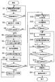
図5は、送電時の電力伝送装置の一例の処理の流れを示すフローチャートである。
制御回路31は、検出センサ34−1〜34−4により、受電装置の検知処理を行い、受電装置の台数を検出する(ステップS1)。たとえば、検出センサ34−1〜34−4の少なくとも1つによって、受電装置の検出センサ(たとえば、図3の検出センサ40d,41d)との間で通信が発生した場合、制御回路31は存在する受電装置の台数を検出する。
Hereinafter, the process of the
FIG. 5 is a flowchart illustrating a flow of processing of an example of the power transmission device during power transmission.
The
そして、制御回路31は、検知処理の結果から受電装置があるか否かを判定する(ステップS2)。受電装置がある場合には、ステップS3の処理が行われ、受電装置がない場合には、ステップS1の処理が継続される。
And the
ステップS3の処理では、検出センサ34−1〜34−4は、検知された受電装置から、その受電装置が正当な送電先か否かを認証するための認証用データを受信する(ステップS3)。認証用データとしては、たとえば、受信した受電装置の型式や、受電装置を所持するユーザの契約情報などがある。 In the process of step S3, the detection sensors 34-1 to 34-4 receive authentication data for authenticating whether or not the power receiving apparatus is a valid power transmission destination from the detected power receiving apparatus (step S3). . The authentication data includes, for example, the type of the received power receiving device and contract information of the user who owns the power receiving device.
ステップS4の処理において、制御回路31は、検出センサ34−1〜34−4が受信した認証用データをもとに、送電先が正当なものか否かを判定する。ここでは、制御回路31は、たとえば、検出センサ34−1〜34−4が受信した認証用データと、記憶部36に格納されている情報との照合を行い、受電装置が正当な送電先であるか否かを判定する。
In the process of step S4, the
正当な送電先と判定された場合には、ステップS5の処理が行われ、正当な送電先ではないと判定された場合には、送電アンプ33は電力を生成せず、ステップS1の処理が行われる。
If it is determined that the power transmission destination is valid, the process of step S5 is performed. If it is determined that the power transmission destination is not valid, the
ステップS5の処理において、制御回路31の制御のもと、検出センサ34−1〜34−4は、正当な送電先と判定された受電装置との間で送受電条件情報の交換を行う。送受電条件情報としては、受電装置のバッテリが対応している電圧やワット数などのバッテリ情報、電力伝送装置30の送電アンプ33の周波数などである。
In the process of step S5, under the control of the
その後、制御回路31は、検出された受電装置の台数に基づき、整合回路35のコンデンサ素子C1〜C3とインダクタ素子L1〜L3の組の選択を行う(ステップS6)。
たとえば、図3に示すように2台の受電装置40,41が検出された場合には、台数が2台のときに用いられるコンデンサ素子とインダクタ素子の組が選択されるように、制御回路31は、整合回路35のスイッチ35a,35bを切り替える。
Thereafter, the
For example, as shown in FIG. 3, when two
その後、制御回路31の制御のもと送電アンプ33は、試行用の送電を開始する(ステップS7)。試行用の送電は、前述したように、本送電時よりも小さい電力で行う。
その後、検出センサ34−1〜34−4は、受電装置と通信を行い、受電装置のバッテリの充電状態や、受電装置が送電可能な範囲内から外れていないかなどの送受電状態情報の交換を行う(ステップS8)。
Thereafter, the
After that, the detection sensors 34-1 to 34-4 communicate with the power receiving apparatus, and exchange power transmission / reception state information such as the state of charge of the battery of the power receiving apparatus and whether the power receiving apparatus is out of the power transmission range. Is performed (step S8).
試行用の送電時において、電力伝送装置30の制御回路31は、図3のノードN1における反射係数を検出し(ステップS9)、反射係数が規定値以上(たとえば、0.2以上(=定在波比が1.5以上))か、否かを判定する(ステップS10)。
During trial power transmission, the
反射係数が規定値以上の場合、制御回路31は、反射係数が減少してインピーダンス整合するように、整合回路35の可変コンデンサCvを調整し(ステップS11)、ステップS9からの処理を繰り返す。
When the reflection coefficient is equal to or greater than the specified value, the
反射係数が規定値以上ではない場合、制御回路31は、受電装置の台数に応じて、送電アンプ33が生成する電力レベルを変更し(ステップS12)、本送電を開始させる(ステップS13)。ここで制御回路31は、電力伝送装置30の各部を検査し不具合が発生していないか判定する(ステップS14)。制御回路31は、不具合がなければ、送電を継続させる(ステップS15)。不具合がある場合には、ステップS20の処理が行われ、送電が停止される。
If the reflection coefficient is not equal to or greater than the specified value, the
本送電中においても、試行用の送電時と同様に、送受電状態情報の交換が定期的に行われる(ステップS16)。制御回路31は、送受電状態情報をもとに、検出された受電装置が送電可能な範囲に存在するか否かを判定する(ステップS17)。受電装置がある場合には、ステップS18の処理が行われ、受電装置がない場合には、ステップS20の処理が行われ、送電が停止される。
Even during the main power transmission, the power transmission / reception state information is periodically exchanged as in the trial power transmission (step S16). Based on the power transmission / reception state information, the
ステップS18の処理において、制御回路31は、送受電状態情報をもとに、受電装置のバッテリに空き容量があるか否かを判定する(ステップS18)。たとえば、検出センサ34−1〜34−4の何れかが、受電装置からバッテリが満充電である旨の送受電状態情報を受信すると、制御回路31は、受電装置のバッテリに空き容量がないと判定し、ステップS20の処理を行う。満充電である旨の送受電状態情報が受信されていない状態では、制御回路31は、受電装置のバッテリは空き容量があると判定し、ステップS19の処理を行う。
In the process of step S18, the
ステップS19の処理において、制御回路31は、送受電状態情報として、受電装置から充電を休止する旨の休止信号が送られてきていないか判定する。休止信号がある場合には、制御回路31は、ステップS20の処理を行う。休止信号がない場合には、制御回路31は、ステップS15の処理を行い、送電を継続させる。
In the process of step S <b> 19, the
ステップ20の処理では、制御回路31は、送電アンプ33による送電を停止させる。その後、制御回路31は、検出センサ34−1〜34−4による通信処理を終了させる(ステップS21)。
In the process of
なお、上記の各ステップの順番は、特に限定されているわけではない。たとえば、ステップS17〜S18の判定処理などは適宜順番を入れ替えてもよい。
以上のように、検出された受電装置の台数に応じて、台数に対応して設けられたコンデンサ素子とインダクタ素子の組を選択することで、適切なインピーダンスを迅速に選択できるようになる。これにより、インピーダンス整合が容易になり、効率的に適切な電力を受電装置に給電することができるようになる。
Note that the order of the above steps is not particularly limited. For example, the order of the determination processes in steps S17 to S18 may be appropriately changed.
As described above, an appropriate impedance can be quickly selected by selecting a combination of a capacitor element and an inductor element provided corresponding to the number of power receiving devices detected. Thereby, impedance matching becomes easy, and appropriate power can be efficiently supplied to the power receiving apparatus.
また、複数のコンデンサ素子C1〜C3とインダクタ素子L1〜L3の組の切り替えにより受電装置の台数に応じたインピーダンス整合を行うので、電力伝送装置30の小型化が期待できる。
Moreover, since impedance matching according to the number of power receiving apparatuses is performed by switching a set of a plurality of capacitor elements C1 to C3 and inductor elements L1 to L3, the
また、可変コンデンサCvを用い、コンデンサ素子C1〜C3とインダクタ素子L1〜L3の組の切り替えにより離散的に変化するインピーダンスを補償することで、より精度よくインピーダンス整合を行うことができる。この可変コンデンサCvは、インピーダンスの微調整を行うものであるので、小さな容積のもので済み、電力伝送装置30の大型化を抑制できる。
Further, by using the variable capacitor Cv and compensating the impedance that changes discretely by switching the set of the capacitor elements C1 to C3 and the inductor elements L1 to L3, impedance matching can be performed with higher accuracy. Since the variable capacitor Cv performs fine adjustment of impedance, the variable capacitor Cv only needs to have a small volume, and the
(実施例)
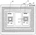
図6は、3台の受電装置に送電を行う電力伝送装置の一例を示す図である。
図6では、図3に示した電力伝送装置30の一例の上面図を示し、受電装置である3台の携帯電話50,51,52に送電を行う場合を示している。図6では共振コイル32a、誘導コイル32bを示しているが、図3の電力伝送装置30のその他の構成については、図示を省略している。
(Example)
FIG. 6 is a diagram illustrating an example of a power transmission device that transmits power to three power receiving devices.
FIG. 6 illustrates a top view of an example of the
携帯電話50〜52は、それぞれ、共振コイル50a,51a,52aと、誘導コイル50b,51b,52bを有している。図示を省略しているが、携帯電話50〜52は、図3に示した受電装置40,41のように、バッテリと検出センサを内蔵している。
Each of the
このような、電力伝送装置30において、送電アンプ33(図3参照)のインピーダンスZSをZS=50Ωとした。3台の携帯電話50〜52に送電する際、共振コイル32aと誘導コイル32bを含む送電コイル32の入力インピーダンスZLがZL=677.5+262.5iΩであったとする。この場合、図3に示した整合回路35においてインダクタ素子でのインダクタンスLMをLM=15.20μH、コンデンサ素子でのキャパシタンスCMをCM=429.6pFとすれば、ノードN1での反射係数を0とすることができる。
In such a
したがって、図3の整合回路35のインダクタ素子L1〜L3の何れかを、インダクタンスが15.20μHである素子とし、コンデンサ素子C1〜C3の何れかを、キャパシタンスが429.6pFである素子として、これらの素子の組を3台用の組とする。
Therefore, any one of the inductor elements L1 to L3 of the matching
なお、誤差は可変コンデンサCvで調整することができるため、必ずしも上記の値に完全に一致させたインダクタ素子L1〜L3またはコンデンサ素子C1〜C3を用意しなくてもよい。 Since the error can be adjusted by the variable capacitor Cv, it is not always necessary to prepare the inductor elements L1 to L3 or the capacitor elements C1 to C3 that completely match the above values.
図7は、受電装置の台数を1台に変更した場合の例を示す図である。
図7では、送電対象の受電装置が、1台の携帯電話51に変更された場合が示されている。
FIG. 7 is a diagram illustrating an example when the number of power receiving apparatuses is changed to one.
FIG. 7 shows a case where the power receiving device to be transmitted is changed to one
このとき、共振コイル32aと誘導コイル32bを含む送電コイル32の入力インピーダンスZLがZL=1680.4+496.4iΩに変化したとする。この場合、前述した3台用のインダクタ素子(LM=15.20μH)とコンデンサ素子(CM=429.6pF)の組を用いると、ノードN1での反射係数は0.435となる。
At this time, it is assumed that the input impedance Z L of the
この反射係数を0にするには、整合回路35においてインダクタ素子でのインダクタンスLMをLM=23.72μH、コンデンサ素子でのキャパシタンスCMをCM=272.5pFとすればよい。
In order to set the reflection coefficient to 0, the inductance L M at the inductor element in the
したがって、図3の整合回路35のインダクタ素子L1〜L3の何れかを、インダクタンスが23.72μHである素子とし、コンデンサ素子C1〜C3の何れかを、キャパシタンスが272.5pFである素子として、これらの素子の組を1台用の組としておく。
Therefore, any one of the inductor elements L1 to L3 of the matching
そして、図3の検出センサ34−1〜34−4からの信号に基づいて、制御回路31が携帯電話の台数が1台に変更されたことを検出すると、制御回路31は、整合回路35のスイッチ35a,35bを切り替えて、上記の1台用の組を選択する。これにより、反射係数を0に近づけ、インピーダンス整合を行うことができる。
When the
なお、誤差は可変コンデンサCvで調整することができるため、必ずしも上記の値に完全に一致させたインダクタ素子L1〜L3またはコンデンサ素子C1〜C3を用意しなくてもよい。 Since the error can be adjusted by the variable capacitor Cv, it is not always necessary to prepare the inductor elements L1 to L3 or the capacitor elements C1 to C3 that completely match the above values.
また、電力伝送装置30と受電装置との位置ずれや送電時の環境などの影響で、予め決めておいたインダクタ素子とコンデンサ素子の組では、反射係数を0にすることができない場合も、可変コンデンサCvで調整して0に近づけることができる。
Further, even when the reflection coefficient cannot be reduced to 0 with a predetermined combination of an inductor element and a capacitor element due to the influence of the positional deviation between the
図8は、受電装置の位置が変化した様子を示した図である。
図8では、受電装置である携帯電話51が、矢印A方向に移動した様子が示されている。1台の携帯電話51で、反射係数が0になるように整合回路35でインダクタ素子とコンデンサ素子の組が選択されている場合、携帯電話51を矢印A方向に50mm移動させたときの反射係数の変動は、たとえば、以下のようになる。
FIG. 8 is a diagram illustrating a change in the position of the power receiving device.
FIG. 8 shows a state in which the
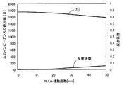
図9は、受電装置の位置の変化に対する反射係数の変動例を示す図である。
図9の横軸では、携帯電話51の移動距離が、コイル(共振コイル51a,誘導コイル51b)移動距離[mm]で表されている。また、左側の縦軸は、電力伝送装置30の送電コイル32での入力インピーダンスの絶対値[Ω]を示し、右側の縦軸は、反射係数の値を示している。
FIG. 9 is a diagram illustrating a variation example of the reflection coefficient with respect to a change in the position of the power receiving apparatus.
In the horizontal axis of FIG. 9, the moving distance of the
図9に示すように、コイル移動距離の増加に伴い、電力伝送装置30の送電コイル32での入力インピーダンスの絶対値|ZL|の値が減少し、反射係数が増加していく。コイル移動距離が50mmの場合には、反射係数は0.05程度となる。実用上、反射係数は0.2以下(=定在波比1.5以下)が望ましいとされるので、この程度であれば、特に問題はないと考えられるが、可変コンデンサCvにより、0に近づけるように調整をおこなってもよい。
As shown in FIG. 9, as the coil moving distance increases, the absolute value | Z L | of the input impedance at the
図10は、受電装置の台数を2台に変更した場合の例を示す図である。
図10では、送電対象の受電装置が、図6に示した3台の携帯電話50〜52から、2台の携帯電話51,52に変更された場合が示されている。
FIG. 10 is a diagram illustrating an example when the number of power receiving apparatuses is changed to two.
FIG. 10 shows a case where the power receiving device to be transmitted is changed from the three
このとき、共振コイル32aと誘導コイル32bを含む送電コイル32の入力インピーダンスZLがZL=911.9+369.5iΩであったとする。この場合、前述した3台用のインダクタ素子(LM=15.20μH)とコンデンサ素子(CM=429.6pF)の組を用いると、ノードN1での反射係数は0.162となる。
At this time, it is assumed that the input impedance Z L of the
この反射係数を0にするには、整合回路35においてインダクタ素子でのインダクタンスLMをLM=17.90μH、コンデンサ素子でのキャパシタンスCMをCM=367.5pFとすればよい。
In order to set the reflection coefficient to 0, the inductance L M at the inductor element in the
したがって、図3の整合回路35のインダクタ素子L1〜L3の何れかを、インダクタンスが17.90μHである素子とし、コンデンサ素子C1〜C3の何れかを、キャパシタンスが367.5pFである素子として、これらの素子の組を2台用の組としておく。
Therefore, any one of the inductor elements L1 to L3 of the matching
そして、図3の検出センサ34−1〜34−4からの信号に基づいて、制御回路31が携帯電話の台数が2台に変更されたことを検出すると、制御回路31は、整合回路35のスイッチ35a,35bを切り替えて、上記の2台用の組を選択する。これにより、反射係数を0に近づけ、インピーダンス整合を行うことができる。
When the
なお、誤差は可変コンデンサCvで調整することができるため、必ずしも上記の値に完全に一致させたインダクタ素子L1〜L3またはコンデンサ素子C1〜C3を用意しなくてもよい。 Since the error can be adjusted by the variable capacitor Cv, it is not always necessary to prepare the inductor elements L1 to L3 or the capacitor elements C1 to C3 that completely match the above values.
図11は、受電装置の位置が変化した様子を示した図である。
図11では、受電装置である携帯電話51が、矢印B方向に移動した様子が示されている。2台の携帯電話51,52で、反射係数が0になるように整合回路35でインダクタ素子とコンデンサ素子の組が選択されている場合、携帯電話51を矢印B方向に50mm移動させたときの反射係数の変動は、たとえば、以下のようになる。
FIG. 11 is a diagram illustrating a state in which the position of the power receiving device has changed.
FIG. 11 shows a state in which the
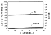
図12は、受電装置の位置の変化に対する反射係数の変動例を示す図である。
図12の横軸では、携帯電話51の移動距離が、コイル(共振コイル51a,誘導コイル51b)移動距離[mm]で表されている。また、左側の縦軸は、電力伝送装置30の送電コイル32での入力インピーダンスの絶対値[Ω]を示し、右側の縦軸は、反射係数の値を示している。
FIG. 12 is a diagram illustrating a variation example of the reflection coefficient with respect to a change in the position of the power receiving apparatus.
In the horizontal axis of FIG. 12, the moving distance of the
図12に示すように、コイル移動距離の増加に伴い、電力伝送装置30の送電コイル32での入力インピーダンスの絶対値|ZL|の値が増加し、反射係数も増加していくが反射係数は0.05以下となる。この程度であれば、特に問題はないと考えられるが、可変コンデンサCvにより、0に近づけるように調整をおこなってもよい。
As shown in FIG. 12, as the coil movement distance increases, the absolute value | Z L | of the input impedance at the
ところで、上記の説明では、整合回路35は、受電装置の台数に対応してインダクタ素子とコンデンサ素子の組が設けられるとしたが、送電距離に応じたインダクタ素子とコンデンサの組を設けてもよい。
In the above description, the matching
図13は、電力伝送装置による、送電距離に応じたインピーダンス整合の一例を説明する図である。
受電装置40と電力伝送装置30との間の送電距離は、たとえば、赤外線センサである検出センサ34−1により測定することができる。
FIG. 13 is a diagram illustrating an example of impedance matching according to the power transmission distance by the power transmission device.
The power transmission distance between the
送電コイル32の入力インピーダンスは、送電距離に応じて変化する。送電距離が変わってもノードN1での反射係数を0に近づけるため、整合回路35は、たとえば、送電距離に応じたインダクタ素子とコンデンサ素子の組を複数有してもよい。
The input impedance of the
たとえば、図13に示すように、受電装置40が1台の場合で、送電距離がR1の範囲のときに反射係数を0に近づけられるインダクタ素子L1とコンデンサ素子C1の組を整合回路35に設けておく。また、受電装置40が1台の場合で、送電距離がR2の範囲で反射係数を0に近づけられるインダクタ素子L2とコンデンサ素子C2の組を整合回路35に予め設けておく。
For example, as shown in FIG. 13, in the case where there is one
たとえば、図13に示すように受電装置40が、R2の範囲に存在する場合、制御回路31は、整合回路35のスイッチ35a,35bを制御して、インダクタ素子L2とコンデンサ素子C2の組を選択させる。これにより、送電距離に応じたインピーダンス整合を、迅速に行うことができる。
For example, as shown in FIG. 13, when the
また、送電距離に応じたインダクタ素子とコンデンサ素子の切替だけでは、反射係数を十分0に近づけることができない場合には、可変コンデンサCvにより調整を行うようにしてもよい。 Further, when the reflection coefficient cannot be sufficiently close to 0 only by switching the inductor element and the capacitor element according to the power transmission distance, the adjustment may be performed by the variable capacitor Cv.
また、図13に示した例では、受電装置40が1台の場合について示したが、複数の場合にも同様に適用できる。たとえば、3台の受電装置が存在し、そのうち2台がR1の範囲に存在し、1台がR2の範囲に存在する場合に、反射係数を0に近づけることができるような、インダクタ素子とコンデンサ素子の組を予め設けるようにしてもよい。
In the example illustrated in FIG. 13, the case where there is one
また、上記では受電装置の種類に応じた整合回路35の制御については説明しなかったが、受電装置の種類や型などに応じて、同じ台数でも異なるインダクタ素子とコンデンサ素子の組を選択するようにしてもよい。
In the above description, the control of the matching
以上、実施の形態に基づき、本発明の一観点について説明してきたが、これらは一例にすぎず、上記の記載に限定されるものではない。
以上説明した複数の実施の形態に関し、さらに以下の付記を開示する。
As mentioned above, although one viewpoint of this invention has been demonstrated based on embodiment, these are only examples and are not limited to said description.
The following additional notes are further disclosed with respect to the plurality of embodiments described above.
(付記1) 受電装置に対して非接触で送電する送電部と、
前記送電部が送電する電力を生成する電源部と、
前記受電装置の台数を検出する検出部と、
前記受電装置の台数に対応したコンデンサ素子とインダクタ素子の組を複数有し、検出された前記受電装置の台数に応じて、選択する前記コンデンサ素子と前記インダクタ素子の組を変更することで前記送電部と前記電源部との間のインピーダンス整合を行う整合部と、
を有することを特徴とする電力伝送装置。
(Supplementary Note 1) A power transmission unit that transmits power to a power receiving device in a contactless manner;
A power supply unit that generates power to be transmitted by the power transmission unit;
A detection unit for detecting the number of the power receiving devices;
There are a plurality of sets of capacitor elements and inductor elements corresponding to the number of the power receiving apparatuses, and the power transmission is performed by changing the set of the capacitor elements and the inductor elements to be selected according to the detected number of the power receiving apparatuses. A matching unit for impedance matching between the power source unit and the power source unit;
A power transmission device comprising:
(付記2) 前記整合部において、前記受電装置の台数に対応した前記コンデンサ素子と前記インダクタ素子の組は、当該台数の場合に、前記送電部と前記電源部との間でインピーダンス整合されるようにキャパシタンス及びインダクタンスが設定されていることを特徴とする付記1記載の電力伝送装置。
(Supplementary Note 2) In the matching unit, a set of the capacitor element and the inductor element corresponding to the number of the power receiving devices is impedance-matched between the power transmission unit and the power supply unit in the case of the number. The power transmission device according to
(付記3) 前記整合部は、前記受電装置の台数に応じた前記コンデンサ素子と前記インダクタ素子の組の変更後、インピーダンスの調整を行う可変コンデンサをさらに有することを特徴とする付記1または2に記載の電力伝送装置。
(Supplementary note 3) The
(付記4) 前記整合部は、前記電源部の出力端の反射係数が規定値以上の場合に、前記可変コンデンサの調整を行うことを特徴とする付記3記載の電力伝送装置。
(付記5) 前記整合部は、前記受電装置に対する送電距離に対応したコンデンサ素子とインダクタ素子の組を複数有し、検出された前記受電装置に対する送電距離に応じて、選択する前記コンデンサ素子と前記インダクタ素子の組を変更することで前記送電部と前記電源部との間のインピーダンス整合を行うことを特徴とする付記1乃至4の何れか一つに記載の電力伝送装置。
(Additional remark 4) The said matching part adjusts the said variable capacitor, when the reflection coefficient of the output terminal of the said power supply part is more than a regulation value, The electric power transmission apparatus of Additional remark 3 characterized by the above-mentioned.
(Additional remark 5) The said matching part has two or more sets of the capacitor | condenser element and inductor element corresponding to the power transmission distance with respect to the said power receiving apparatus, The said capacitor element to select according to the detected power transmission distance with respect to the said power receiving apparatus, and the said The power transmission device according to any one of
(付記6) 前記電源部は、検出された前記受電装置の台数に応じて生成する電力の大きさを変更することを特徴とする付記1乃至5の何れか一つに記載の電力伝送装置。
(付記7) 前記送電部は、磁界共鳴方式で前記受電装置に対して送電を行うことを特徴とする付記1乃至6の何れか一つに記載の電力伝送装置。
(Additional remark 6) The said power supply part changes the magnitude | size of the electric power produced | generated according to the detected number of the said power receiving apparatuses, The power transmission apparatus as described in any one of
(Additional remark 7) The said power transmission part transmits electric power with respect to the said power receiving apparatus by a magnetic field resonance system, The power transmission apparatus as described in any one of
(付記8) 受電装置の台数を検出し、
それぞれ前記受電装置の台数に対応したコンデンサ素子とインダクタ素子の複数の組の何れかを、検出された前記受電装置の台数に応じて選択して、前記受電装置に対して非接触で送電する送電部と前記送電部が送電する電力を生成する電源部との間のインピーダンス整合を行うことを特徴とする電力伝送方法。
(Appendix 8) Detect the number of power receiving devices,
Power transmission for transmitting power in a non-contact manner to the power receiving device by selecting one of a plurality of sets of capacitor elements and inductor elements corresponding to the number of the power receiving devices according to the detected number of the power receiving devices. A power transmission method comprising performing impedance matching between a power supply unit that generates power transmitted by the power transmission unit and the power transmission unit.
10 電力伝送装置
11 送電部
12 電源部
13 検出部
14 整合部
14a,14b スイッチ
20,21 受電装置
C1〜C3 コンデンサ素子
L1〜L3 インダクタ素子
DESCRIPTION OF
Claims (5)
前記送電部が送電する電力を生成する電源部と、
前記受電装置の台数を検出する検出部と、
前記受電装置の台数に対応したコンデンサ素子とインダクタ素子の組を複数有し、検出された前記受電装置の台数に応じて、選択する前記コンデンサ素子と前記インダクタ素子の組を変更することで前記送電部と前記電源部との間のインピーダンス整合を行う整合部と、
を有することを特徴とする電力伝送装置。 A power transmission unit that transmits power to the power receiving device in a contactless manner;
A power supply unit that generates power to be transmitted by the power transmission unit;
A detection unit for detecting the number of the power receiving devices;
There are a plurality of sets of capacitor elements and inductor elements corresponding to the number of the power receiving apparatuses, and the power transmission is performed by changing the set of the capacitor elements and the inductor elements to be selected according to the detected number of the power receiving apparatuses. A matching unit for impedance matching between the power source unit and the power source unit;
A power transmission device comprising:
それぞれ前記受電装置の台数に対応したコンデンサ素子とインダクタ素子の複数の組の何れかを、検出された前記受電装置の台数に応じて選択して、前記受電装置に対して非接触で送電する送電部と前記送電部が送電する電力を生成する電源部との間のインピーダンス整合を行うことを特徴とする電力伝送方法。 Detect the number of power receiving devices
Power transmission for transmitting power in a non-contact manner to the power receiving device by selecting one of a plurality of sets of capacitor elements and inductor elements corresponding to the number of the power receiving devices according to the detected number of the power receiving devices. A power transmission method comprising performing impedance matching between a power supply unit that generates power transmitted by the power transmission unit and the power transmission unit.
Priority Applications (1)
| Application Number | Priority Date | Filing Date | Title |
|---|---|---|---|
| JP2011005944A JP2012147632A (en) | 2011-01-14 | 2011-01-14 | Power transmission device and power transmission method |
Applications Claiming Priority (1)
| Application Number | Priority Date | Filing Date | Title |
|---|---|---|---|
| JP2011005944A JP2012147632A (en) | 2011-01-14 | 2011-01-14 | Power transmission device and power transmission method |
Publications (1)
| Publication Number | Publication Date |
|---|---|
| JP2012147632A true JP2012147632A (en) | 2012-08-02 |
Family
ID=46790604
Family Applications (1)
| Application Number | Title | Priority Date | Filing Date |
|---|---|---|---|
| JP2011005944A Pending JP2012147632A (en) | 2011-01-14 | 2011-01-14 | Power transmission device and power transmission method |
Country Status (1)
| Country | Link |
|---|---|
| JP (1) | JP2012147632A (en) |
Cited By (7)
| Publication number | Priority date | Publication date | Assignee | Title |
|---|---|---|---|---|
| JP2014135862A (en) * | 2013-01-11 | 2014-07-24 | Canon Inc | Power feeding device, image forming apparatus, and power feeding method and program |
| JP2015042091A (en) * | 2013-08-22 | 2015-03-02 | キヤノン株式会社 | Power transmission device, power reception device, control method thereof, and program |
| KR20150109875A (en) * | 2014-03-21 | 2015-10-02 | 한양대학교 산학협력단 | Wireless charging transmitter and receiver |
| JP2017093174A (en) * | 2015-11-11 | 2017-05-25 | 清水建設株式会社 | Power feeding system and method for controlling power feeding system |
| JP2018117404A (en) * | 2017-01-16 | 2018-07-26 | 株式会社Soken | Power transmission unit of wireless power feeder |
| JP2019068580A (en) * | 2017-09-29 | 2019-04-25 | 国立大学法人豊橋技術科学大学 | Wireless power supply device, conveyance system using the same, and control method of wireless power supply device |
| WO2025004219A1 (en) * | 2023-06-28 | 2025-01-02 | 三菱電機株式会社 | Power transmission apparatus and non-contact power supply system |
Citations (4)
| Publication number | Priority date | Publication date | Assignee | Title |
|---|---|---|---|---|
| JP2000251029A (en) * | 1999-03-03 | 2000-09-14 | Tamura Electric Works Ltd | Non-contact ic card reader system |
| JP2001238372A (en) * | 2000-02-24 | 2001-08-31 | Nippon Telegr & Teleph Corp <Ntt> | Power transmission system, electromagnetic field generator and electromagnetic field receiver |
| WO2009140220A1 (en) * | 2008-05-13 | 2009-11-19 | Qualcomm Incorporated | Method and apparatus for adaptive tuning of wireless power transfer |
| WO2010093997A1 (en) * | 2009-02-13 | 2010-08-19 | Witricity Corporation | Wireless energy transfer in lossy environments |
-
2011
- 2011-01-14 JP JP2011005944A patent/JP2012147632A/en active Pending
Patent Citations (4)
| Publication number | Priority date | Publication date | Assignee | Title |
|---|---|---|---|---|
| JP2000251029A (en) * | 1999-03-03 | 2000-09-14 | Tamura Electric Works Ltd | Non-contact ic card reader system |
| JP2001238372A (en) * | 2000-02-24 | 2001-08-31 | Nippon Telegr & Teleph Corp <Ntt> | Power transmission system, electromagnetic field generator and electromagnetic field receiver |
| WO2009140220A1 (en) * | 2008-05-13 | 2009-11-19 | Qualcomm Incorporated | Method and apparatus for adaptive tuning of wireless power transfer |
| WO2010093997A1 (en) * | 2009-02-13 | 2010-08-19 | Witricity Corporation | Wireless energy transfer in lossy environments |
Cited By (9)
| Publication number | Priority date | Publication date | Assignee | Title |
|---|---|---|---|---|
| JP2014135862A (en) * | 2013-01-11 | 2014-07-24 | Canon Inc | Power feeding device, image forming apparatus, and power feeding method and program |
| JP2015042091A (en) * | 2013-08-22 | 2015-03-02 | キヤノン株式会社 | Power transmission device, power reception device, control method thereof, and program |
| KR20150109875A (en) * | 2014-03-21 | 2015-10-02 | 한양대학교 산학협력단 | Wireless charging transmitter and receiver |
| KR101599125B1 (en) * | 2014-03-21 | 2016-03-14 | 한양대학교 산학협력단 | Wireless charging transmitter and receiver |
| JP2017093174A (en) * | 2015-11-11 | 2017-05-25 | 清水建設株式会社 | Power feeding system and method for controlling power feeding system |
| JP2018117404A (en) * | 2017-01-16 | 2018-07-26 | 株式会社Soken | Power transmission unit of wireless power feeder |
| JP2019068580A (en) * | 2017-09-29 | 2019-04-25 | 国立大学法人豊橋技術科学大学 | Wireless power supply device, conveyance system using the same, and control method of wireless power supply device |
| WO2025004219A1 (en) * | 2023-06-28 | 2025-01-02 | 三菱電機株式会社 | Power transmission apparatus and non-contact power supply system |
| JPWO2025004219A1 (en) * | 2023-06-28 | 2025-01-02 |
Similar Documents
| Publication | Publication Date | Title |
|---|---|---|
| US9997930B2 (en) | Wireless power transmission apparatus and wireless power transfer system | |
| US9634493B2 (en) | Resonant frequency control method, electric power transmitting device, electric power receiving device in magnetic resonant type power transmission system | |
| JP2012147632A (en) | Power transmission device and power transmission method | |
| CN105048644B (en) | Wireless power transmitter, wireless power receiver, and wireless power transmission method | |
| EP2525461B1 (en) | Wireless power receiver and method for controlling the same | |
| JP5863261B2 (en) | Power receiving apparatus and wireless power transmitting / receiving system | |
| JP5839629B1 (en) | Non-contact communication device, antenna circuit, antenna drive device, non-contact power supply device, tuning method, discovery method, and program for realizing these methods | |
| CN105281441B (en) | Wireless power transmitter and Wireless power transmission system | |
| US20180254668A1 (en) | Resonant contactless power supply equipment, electrical transmitter and contactless power supply method | |
| JP6135762B2 (en) | Power transmission device and power transmission method | |
| US10389162B2 (en) | Power receiving unit reflected reactance and tuning methods | |
| EP3130070B1 (en) | Inductive power transfer converters and system | |
| CN110556925B (en) | Wireless charger and control method | |
| US9148024B2 (en) | Apparatuses, systems, and methods for a monotonic transfer function in wireless power transfer systems | |
| US20150333537A1 (en) | Power source, wireless power transfer system and wireless power transfer method | |
| US20160285280A1 (en) | Auxiliary receiver coil to adjust receiver voltage and reactance | |
| JP6535003B2 (en) | Wireless power receiver | |
| US9130409B2 (en) | Wireless energy receiver/transmitter/system and wireless energy transmission method | |
| WO2013132546A1 (en) | Communication apparatus | |
| US20170133860A1 (en) | System And Method Of Wireless Power Transfer Without Data Communication Channel | |
| JP5996753B2 (en) | Discovery method and program thereof | |
| KR20150055755A (en) | Hybrid wireless power transmission device which enables to transmit resonance power signal and induced power signal simultaneously and hybrid wireless power transmission system including the same | |
| JP5808849B1 (en) | Control method, contactless communication device, contactless power supply device, program, and drive circuit | |
| US20180080999A1 (en) | Determining power electronics feasibility with single turn magnetic simulation data | |
| JP5454590B2 (en) | Resonance frequency control method, power transmission device, and power reception device in magnetic resonance power transmission system |
Legal Events
| Date | Code | Title | Description |
|---|---|---|---|
| A621 | Written request for application examination |
Free format text: JAPANESE INTERMEDIATE CODE: A621 Effective date: 20131007 |
|
| A977 | Report on retrieval |
Free format text: JAPANESE INTERMEDIATE CODE: A971007 Effective date: 20140625 |
|
| A131 | Notification of reasons for refusal |
Free format text: JAPANESE INTERMEDIATE CODE: A131 Effective date: 20140701 |
|
| A521 | Written amendment |
Free format text: JAPANESE INTERMEDIATE CODE: A523 Effective date: 20140829 |
|
| A02 | Decision of refusal |
Free format text: JAPANESE INTERMEDIATE CODE: A02 Effective date: 20141111 |