JP2012155221A - 撮像装置及びその制御方法 - Google Patents
撮像装置及びその制御方法 Download PDFInfo
- Publication number
- JP2012155221A JP2012155221A JP2011015706A JP2011015706A JP2012155221A JP 2012155221 A JP2012155221 A JP 2012155221A JP 2011015706 A JP2011015706 A JP 2011015706A JP 2011015706 A JP2011015706 A JP 2011015706A JP 2012155221 A JP2012155221 A JP 2012155221A
- Authority
- JP
- Japan
- Prior art keywords
- divided
- image
- pupil division
- pupil
- pixel
- Prior art date
- Legal status (The legal status is an assumption and is not a legal conclusion. Google has not performed a legal analysis and makes no representation as to the accuracy of the status listed.)
- Granted
Links
Images



Classifications
-
- H—ELECTRICITY
- H04—ELECTRIC COMMUNICATION TECHNIQUE
- H04N—PICTORIAL COMMUNICATION, e.g. TELEVISION
- H04N23/00—Cameras or camera modules comprising electronic image sensors; Control thereof
- H04N23/60—Control of cameras or camera modules
- H04N23/67—Focus control based on electronic image sensor signals
- H04N23/672—Focus control based on electronic image sensor signals based on the phase difference signals
-
- H—ELECTRICITY
- H04—ELECTRIC COMMUNICATION TECHNIQUE
- H04N—PICTORIAL COMMUNICATION, e.g. TELEVISION
- H04N25/00—Circuitry of solid-state image sensors [SSIS]; Control thereof
- H04N25/40—Extracting pixel data from image sensors by controlling scanning circuits, e.g. by modifying the number of pixels sampled or to be sampled
- H04N25/46—Extracting pixel data from image sensors by controlling scanning circuits, e.g. by modifying the number of pixels sampled or to be sampled by combining or binning pixels
-
- H—ELECTRICITY
- H04—ELECTRIC COMMUNICATION TECHNIQUE
- H04N—PICTORIAL COMMUNICATION, e.g. TELEVISION
- H04N25/00—Circuitry of solid-state image sensors [SSIS]; Control thereof
- H04N25/70—SSIS architectures; Circuits associated therewith
- H04N25/703—SSIS architectures incorporating pixels for producing signals other than image signals
- H04N25/704—Pixels specially adapted for focusing, e.g. phase difference pixel sets
-
- H—ELECTRICITY
- H04—ELECTRIC COMMUNICATION TECHNIQUE
- H04N—PICTORIAL COMMUNICATION, e.g. TELEVISION
- H04N25/00—Circuitry of solid-state image sensors [SSIS]; Control thereof
- H04N25/70—SSIS architectures; Circuits associated therewith
- H04N25/76—Addressed sensors, e.g. MOS or CMOS sensors
- H04N25/77—Pixel circuitry, e.g. memories, A/D converters, pixel amplifiers, shared circuits or shared components
- H04N25/778—Pixel circuitry, e.g. memories, A/D converters, pixel amplifiers, shared circuits or shared components comprising amplifiers shared between a plurality of pixels, i.e. at least one part of the amplifier must be on the sensor array itself
-
- H—ELECTRICITY
- H04—ELECTRIC COMMUNICATION TECHNIQUE
- H04N—PICTORIAL COMMUNICATION, e.g. TELEVISION
- H04N25/00—Circuitry of solid-state image sensors [SSIS]; Control thereof
- H04N25/70—SSIS architectures; Circuits associated therewith
- H04N25/702—SSIS architectures characterised by non-identical, non-equidistant or non-planar pixel layout
Landscapes
- Engineering & Computer Science (AREA)
- Multimedia (AREA)
- Signal Processing (AREA)
- Automatic Focus Adjustment (AREA)
- Focusing (AREA)
- Studio Devices (AREA)
Abstract
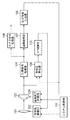
【解決手段】 複数の瞳領域に画素内瞳分割された複数の分割画素を有し、分割画素毎に、水平及び垂直方向に瞳分割して電荷を加算読み出し可能な撮像素子(103)と、画素毎の画像信号に基づいて、撮像素子の領域を複数に分割した分割領域毎に画像のエッジの方向を判定する画素解析部(107)と、判定されたエッジの方向に基づいて、分割領域毎に、水平及び垂直方向の何れかを瞳分割方向として決定する指示情報生成部(108)と、決定された瞳分割方向に分割して、各分割画素の加算読み出しを行い、対の画像信号を出力するように撮像素子を制御する撮像素子駆動部(104)と、各分割画素から出力された対の画像信号の位相差に基づいて、焦点調節を行う焦点調節手段(102、109、110)とを有する。
【選択図】 図1
Description
x = i × HSIZE + x'
y = j × VSIZE + y' …(1)
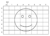
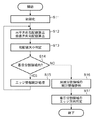
画像解析部107には、分割領域アドレス(i, j)と加算画像信号のアドレス(x, y)とが共に入力される。まず、画像解析部107による分割領域毎の被写体情報(被写体の画像のエッジ方向の情報)の生成方法について説明する。
i × HSIZE ≦ x < (i + 1) × HSIZE
j × VSIZE ≦ y < (i + 1) × VSIZE …(2)
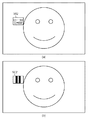
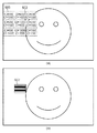
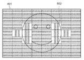
図11は、着目分割領域502で求められた統計情報と、その周囲の分割領域503の統計情報から決定したエッジ方向の一例を示す図である。図11(a)は、着目分割領域502、及びその周囲の着目分割領域群503の統計情報を示しており、式(3)及び式(4)に基づいて合成値を算出すると、合成値C1’>合成値C0’である。そのため、図11(b)に示すように、合成値の関係から、エッジ方向判定部407は、着目分割領域502のエッジ方向は水平であると判定する。
Claims (8)
- 光学系の射出瞳の異なる領域を通った光束をそれぞれ受光する2次元に配置された複数の光電変換部をそれぞれ含む、複数の分割画素を有し、前記分割画素毎に、第1の瞳分割方向及び該第1の瞳分割方向に垂直な第2の瞳分割方向に前記光電変換部を分けて、生成された電荷を加算読み出し可能な撮像素子と、
前記撮像素子から読み出した電荷から得られた画素毎の画像信号に基づいて、前記撮像素子の領域を複数に分割した分割領域毎に画像のエッジの方向を判定する判定手段と、
前記判定手段により前記分割領域毎に判定されたエッジの方向に基づいて、前記分割領域毎に、前記第1の瞳分割方向と前記第2の瞳分割方向の何れかを決定する決定手段と、
前記決定手段により決定された前記第1の瞳分割方向または前記第2の瞳分割方向に分割して、前記各分割画素の加算読み出しを行い、対の画像信号を出力するように前記撮像素子を制御する読み出し制御手段と、
前記読み出し制御手段による制御により前記各分割画素から出力された対の画像信号の位相差に基づいて、焦点調節を行う焦点調節手段と
を有することを特徴とする撮像装置。 - 前記判定手段は、エッジの方向として、前記第1の瞳分割方向に垂直な第1の方向と、前記第2の瞳分割方向に垂直な第2の方向のいずれかであるかを判定することを特徴とする請求項1に記載の撮像装置。
- 前記決定手段は、前記エッジの方向が前記第1の方向である場合に、前記第1の瞳分割方向を決定し、前記エッジの方向が前記第2の方向である場合に、前記第2の瞳分割方向を決定することを特徴とする請求項2に記載の撮像装置。
- 前記決定手段は、前記エッジの方向がより水平に近い場合に、前記第1の瞳分割方向を決定し、前記エッジの方向がより垂直に近い場合に、前記第2の瞳分割方向を決定することを特徴とする請求項1に記載の撮像装置。
- 前記撮像素子を構成する全画素を、前記分割画素で構成したことを特徴とする請求項1乃至4のいずれか1項に記載の撮像装置。
- 前記撮像素子は、1つの光電変換部をそれぞれ含む複数の画素と、離散的に配置された複数の前記分割画素とから構成されていることを特徴とする請求項1乃至4のいずれか1項に記載の撮像装置。
- 前記対の画像信号を、前記分割画素毎に加算する加算手段を更に有することを特徴とする請求項1乃至6のいずれか1項に記載の撮像装置。
- 光学系の射出瞳の異なる領域を通った光束をそれぞれ受光する2次元に配置された複数の光電変換部をそれぞれ含む、複数の分割画素を有し、前記分割画素毎に、第1の瞳分割方向及び該第1の瞳分割方向に垂直な第2の瞳分割方向に前記光電変換部を分けて、生成された電荷を加算読み出し可能な撮像素子を有する撮像装置の制御方法であって、
判定手段が、前記撮像素子から読み出した電荷から得られた画素毎の画像信号に基づいて、前記撮像素子の領域を複数に分割した分割領域毎に画像のエッジの方向を判定する判定工程と、
決定手段が、前記判定工程で前記分割領域毎に判定されたエッジの方向に基づいて、前記分割領域毎に、前記第1の瞳分割方向と前記第2の瞳分割方向の何れかを決定する決定工程と、
読み出し制御手段が、前記決定工程で決定された前記第1の瞳分割方向または前記第2の瞳分割方向に分割して、前記各分割画素の加算読み出しを行い、対の画像信号を出力するように前記撮像素子を制御する読み出し制御工程と、
焦点調節手段が、前記読み出し制御工程による制御により前記各分割画素から出力された対の画像信号の位相差に基づいて、焦点調節を行う焦点調節工程と
を有することを特徴とする撮像装置の制御方法。
Priority Applications (2)
| Application Number | Priority Date | Filing Date | Title |
|---|---|---|---|
| JP2011015706A JP5856376B2 (ja) | 2011-01-27 | 2011-01-27 | 撮像装置及びその制御方法 |
| US13/352,945 US8749697B2 (en) | 2011-01-27 | 2012-01-18 | Image capturing apparatus and control method thereof |
Applications Claiming Priority (1)
| Application Number | Priority Date | Filing Date | Title |
|---|---|---|---|
| JP2011015706A JP5856376B2 (ja) | 2011-01-27 | 2011-01-27 | 撮像装置及びその制御方法 |
Publications (3)
| Publication Number | Publication Date |
|---|---|
| JP2012155221A true JP2012155221A (ja) | 2012-08-16 |
| JP2012155221A5 JP2012155221A5 (ja) | 2014-03-13 |
| JP5856376B2 JP5856376B2 (ja) | 2016-02-09 |
Family
ID=46577076
Family Applications (1)
| Application Number | Title | Priority Date | Filing Date |
|---|---|---|---|
| JP2011015706A Active JP5856376B2 (ja) | 2011-01-27 | 2011-01-27 | 撮像装置及びその制御方法 |
Country Status (2)
| Country | Link |
|---|---|
| US (1) | US8749697B2 (ja) |
| JP (1) | JP5856376B2 (ja) |
Cited By (4)
| Publication number | Priority date | Publication date | Assignee | Title |
|---|---|---|---|---|
| WO2016111175A1 (ja) * | 2015-01-07 | 2016-07-14 | ソニー株式会社 | 画像処理装置、画像処理方法、及び、プログラム |
| JPWO2017169479A1 (ja) * | 2016-03-31 | 2019-01-31 | 株式会社ニコン | 撮像素子、及び、撮像装置 |
| JP2020141206A (ja) * | 2019-02-27 | 2020-09-03 | キヤノン株式会社 | 撮像素子、撮像装置および撮像素子の制御方法 |
| WO2021158043A1 (ko) * | 2020-02-04 | 2021-08-12 | 삼성전자 주식회사 | 전자 장치 및 오토 포커스 수행 방법 |
Families Citing this family (15)
| Publication number | Priority date | Publication date | Assignee | Title |
|---|---|---|---|---|
| EP2833623B1 (en) * | 2012-03-30 | 2019-09-18 | Nikon Corporation | Image sensor, imaging method, and imaging device |
| WO2014077065A1 (ja) * | 2012-11-14 | 2014-05-22 | 富士フイルム株式会社 | 画像処理装置、撮像装置、画像処理方法及び画像処理プログラム |
| JP2014106476A (ja) * | 2012-11-29 | 2014-06-09 | Canon Inc | 焦点検出装置、撮像装置、撮像システム、焦点検出方法、プログラム、および、記憶媒体 |
| JP6346439B2 (ja) * | 2013-01-07 | 2018-06-20 | キヤノン株式会社 | 撮像装置及びその制御方法 |
| US9402069B2 (en) * | 2013-06-07 | 2016-07-26 | Canon Kabushiki Kaisha | Depth measurement apparatus, imaging apparatus, and method of controlling depth measurement apparatus |
| US20140362190A1 (en) * | 2013-06-07 | 2014-12-11 | Canon Kabushiki Kaisha | Depth measurement apparatus, imaging apparatus, and method of controlling depth measurement apparatus |
| JP6207243B2 (ja) * | 2013-06-07 | 2017-10-04 | キヤノン株式会社 | 測距装置、撮像装置及び測距装置の制御方法 |
| US9354212B2 (en) * | 2014-01-07 | 2016-05-31 | Applied Materials Israel Ltd. | Inspection having a segmented pupil |
| JP2016038414A (ja) * | 2014-08-05 | 2016-03-22 | キヤノン株式会社 | 焦点検出装置およびその制御方法、並びに撮像装置 |
| JP6553881B2 (ja) * | 2015-02-05 | 2019-07-31 | キヤノン株式会社 | 画像処理装置 |
| US9787889B2 (en) * | 2015-02-12 | 2017-10-10 | Semiconductor Components Industries, Llc | Dynamic auto focus zones for auto focus pixel systems |
| KR20170056909A (ko) | 2015-11-16 | 2017-05-24 | 삼성전자주식회사 | 이미지 센서 및 이를 포함하는 전자 장치 |
| JP6727017B2 (ja) * | 2016-04-21 | 2020-07-22 | キヤノン株式会社 | 撮像装置及びその制御方法、及び、画像処理装置及び画像処理方法 |
| JP2017195584A (ja) * | 2016-04-22 | 2017-10-26 | キヤノン株式会社 | 撮像装置 |
| EP4270934B1 (en) * | 2021-02-10 | 2026-04-01 | Samsung Electronics Co., Ltd. | Electronic device comprising image sensor and method of operating same |
Citations (5)
| Publication number | Priority date | Publication date | Assignee | Title |
|---|---|---|---|---|
| JP2002314062A (ja) * | 2001-04-18 | 2002-10-25 | Canon Inc | 固体撮像装置および撮像システム |
| JP2007103590A (ja) * | 2005-10-03 | 2007-04-19 | Nikon Corp | 撮像素子、焦点検出装置、および、撮像システム |
| JP2007325139A (ja) * | 2006-06-03 | 2007-12-13 | Nikon Corp | 固体撮像素子及びこれを用いた撮像装置 |
| JP2009094881A (ja) * | 2007-10-10 | 2009-04-30 | Nikon Corp | 撮像装置および撮像方法 |
| JP2010020016A (ja) * | 2008-07-09 | 2010-01-28 | Canon Inc | 撮像装置 |
Family Cites Families (3)
| Publication number | Priority date | Publication date | Assignee | Title |
|---|---|---|---|---|
| JP4770560B2 (ja) * | 2006-04-11 | 2011-09-14 | 株式会社ニコン | 撮像装置、カメラおよび画像処理方法 |
| JP2011039499A (ja) * | 2009-07-14 | 2011-02-24 | Hoya Corp | 自動焦点検出装置 |
| JP5753371B2 (ja) * | 2010-11-25 | 2015-07-22 | キヤノン株式会社 | 撮像装置およびその制御方法 |
-
2011
- 2011-01-27 JP JP2011015706A patent/JP5856376B2/ja active Active
-
2012
- 2012-01-18 US US13/352,945 patent/US8749697B2/en active Active
Patent Citations (5)
| Publication number | Priority date | Publication date | Assignee | Title |
|---|---|---|---|---|
| JP2002314062A (ja) * | 2001-04-18 | 2002-10-25 | Canon Inc | 固体撮像装置および撮像システム |
| JP2007103590A (ja) * | 2005-10-03 | 2007-04-19 | Nikon Corp | 撮像素子、焦点検出装置、および、撮像システム |
| JP2007325139A (ja) * | 2006-06-03 | 2007-12-13 | Nikon Corp | 固体撮像素子及びこれを用いた撮像装置 |
| JP2009094881A (ja) * | 2007-10-10 | 2009-04-30 | Nikon Corp | 撮像装置および撮像方法 |
| JP2010020016A (ja) * | 2008-07-09 | 2010-01-28 | Canon Inc | 撮像装置 |
Cited By (6)
| Publication number | Priority date | Publication date | Assignee | Title |
|---|---|---|---|---|
| WO2016111175A1 (ja) * | 2015-01-07 | 2016-07-14 | ソニー株式会社 | 画像処理装置、画像処理方法、及び、プログラム |
| JPWO2017169479A1 (ja) * | 2016-03-31 | 2019-01-31 | 株式会社ニコン | 撮像素子、及び、撮像装置 |
| JP2020141206A (ja) * | 2019-02-27 | 2020-09-03 | キヤノン株式会社 | 撮像素子、撮像装置および撮像素子の制御方法 |
| JP7337512B2 (ja) | 2019-02-27 | 2023-09-04 | キヤノン株式会社 | 撮像素子、撮像装置および撮像素子の制御方法 |
| WO2021158043A1 (ko) * | 2020-02-04 | 2021-08-12 | 삼성전자 주식회사 | 전자 장치 및 오토 포커스 수행 방법 |
| US12348865B2 (en) | 2020-02-04 | 2025-07-01 | Samsung Electronics Co., Ltd. | Electronic device, and method for performing autofocus by rotating or reordering AF data |
Also Published As
| Publication number | Publication date |
|---|---|
| US20120194721A1 (en) | 2012-08-02 |
| JP5856376B2 (ja) | 2016-02-09 |
| US8749697B2 (en) | 2014-06-10 |
Similar Documents
| Publication | Publication Date | Title |
|---|---|---|
| JP5856376B2 (ja) | 撮像装置及びその制御方法 | |
| CN103888666B (zh) | 摄像设备 | |
| JP2012155221A5 (ja) | ||
| JP6553881B2 (ja) | 画像処理装置 | |
| JP6351231B2 (ja) | 撮像装置、撮像システム、撮像装置の制御方法、プログラム、および、記憶媒体 | |
| JP2017216646A (ja) | 撮像素子、撮像装置、および撮像信号処理方法 | |
| US11310410B2 (en) | Image capturing apparatus, method of controlling same, and storage medium | |
| US20190182431A1 (en) | Imaging element and imaging device | |
| JP5406889B2 (ja) | 撮像装置及びその制御方法 | |
| JP2015212794A (ja) | 撮像装置、その制御方法、および制御プログラム | |
| JP7522571B2 (ja) | 撮像装置及びその制御方法、プログラム、並びに記憶媒体 | |
| US10225494B2 (en) | Image capturing apparatus and control method thereof | |
| JP2018004689A (ja) | 画像処理装置および方法、および撮像装置 | |
| US20180220058A1 (en) | Image capture apparatus, control method therefor, and computer-readable medium | |
| US10136088B2 (en) | Image pickup apparatus that reduces amount of information of defective pixels, method of controlling the same, and storage medium | |
| US10551591B2 (en) | Imaging apparatus, control method of imaging apparatus, and storage medium storing control program of imaging apparatus for performing focus detection and display | |
| JP2017194654A (ja) | 撮像装置及びその制御方法、プログラム並びに記憶媒体 | |
| US10203206B2 (en) | Image capture apparatus having signal readouts using distance measurement region | |
| JP2015148676A (ja) | 撮像装置及び撮像装置の制御方法 | |
| US12238260B2 (en) | Device, capturing device, control method, and storage medium operable for outputting pair of captured images pertaining to binocular stereopsis | |
| US10122913B2 (en) | Image capturing apparatus and control method thereof, and storage medium | |
| JP2017216649A (ja) | 撮像素子、撮像装置、および撮像信号処理方法 | |
| JP6678505B2 (ja) | 撮像装置及びその制御方法、プログラム並びに記憶媒体 | |
| JP2017034508A (ja) | 撮像素子及びその制御方法、及び、撮像装置 | |
| JP2017022639A (ja) | 画像処理装置、撮像装置および画像処理プログラム |
Legal Events
| Date | Code | Title | Description |
|---|---|---|---|
| A521 | Request for written amendment filed |
Free format text: JAPANESE INTERMEDIATE CODE: A523 Effective date: 20140124 |
|
| A621 | Written request for application examination |
Free format text: JAPANESE INTERMEDIATE CODE: A621 Effective date: 20140124 |
|
| A977 | Report on retrieval |
Free format text: JAPANESE INTERMEDIATE CODE: A971007 Effective date: 20141121 |
|
| A131 | Notification of reasons for refusal |
Free format text: JAPANESE INTERMEDIATE CODE: A131 Effective date: 20141201 |
|
| A521 | Request for written amendment filed |
Free format text: JAPANESE INTERMEDIATE CODE: A523 Effective date: 20150130 |
|
| A131 | Notification of reasons for refusal |
Free format text: JAPANESE INTERMEDIATE CODE: A131 Effective date: 20150703 |
|
| A521 | Request for written amendment filed |
Free format text: JAPANESE INTERMEDIATE CODE: A523 Effective date: 20150831 |
|
| TRDD | Decision of grant or rejection written | ||
| A01 | Written decision to grant a patent or to grant a registration (utility model) |
Free format text: JAPANESE INTERMEDIATE CODE: A01 Effective date: 20151113 |
|
| A61 | First payment of annual fees (during grant procedure) |
Free format text: JAPANESE INTERMEDIATE CODE: A61 Effective date: 20151211 |
|
| R151 | Written notification of patent or utility model registration |
Ref document number: 5856376 Country of ref document: JP Free format text: JAPANESE INTERMEDIATE CODE: R151 |